 | –≠–ª–µ–∫—Ç—Ä–æ–Ω–Ω—ã–π –∫–æ–º–ø–æ–Ω–µ–Ω—Ç: CY2309NZ | –°–∫–∞—á–∞—Ç—å:  PDF PDF  ZIP ZIP |
Nine-Output 3.3V Buffer
CY2309NZ
Cypress Semiconductor Corporation
∑
3901 North First Street
∑
San Jose
,
CA 95134
∑
408-943-2600
Document #: 38-07182 Rev. *C
Revised February 24, 2004
Features
∑ One-input to nine-output buffer/driver
∑ Supports two DIMMs or four SO-DIMMs with one
additional output for feedback to an external or chipset
PLL
∑ Low power consumption for mobile applications
-- Less than 32 mA at 66.6 MHz with unloaded outputs
∑ 8.7-ns Input-Output delay
∑ Buffers all frequencies from DC to 133.33 MHz
∑ Output-output skew less than 250 ps
∑ Multiple V
DD
and V
SS
pins for noise and electromag-
netic interference (EMI) reduction
∑ Space-saving 16-pin 150-mil SOIC package
∑ 3.3V operation
∑ Industrial temperature available
Functional Description
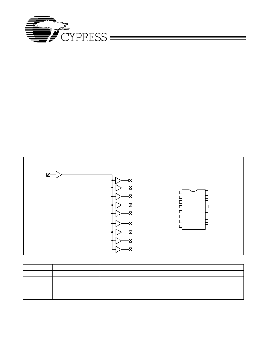
The CY2309NZ is a low-cost buffer designed to distribute
high-speed clocks in mobile PC systems and desktop PC
systems with SDRAM support. The part has nine outputs,
eight of which can be used to drive 2 DIMMs or 4 SO-DIMMs,
and the remaining can be used for external feedback to a PLL.
The device operates at 3.3V and outputs can run up to
133.33 MHz.
The CY2309NZ is designed for low EMI and power optimi-
zation. It has multiple V
SS
and V
DD
pins for noise optimization
and consumes less than 32 mA at 66.6 MHz, making it ideal
for the low-power requirements of mobile systems. It is
available in an ultra-compact 150-mil 16-pin SOIC package.
Block Diagram
1
2
3
4
5
6
7
8
9
10
11
12
13
14
15
16
BUF_IN
OUTPUT1
OUTPUT2
V
DD
GND
OUTPUT3
OUTPUT4
V
DD
OUTPUT9
OUTPUT8
OUTPUT7
V
DD
GND
OUTPUT6
OUTPUT5
GND
16 SOIC
Top View
Pin Configuration
BUF_IN
OUTPUT2
OUTPUT3
OUTPUT4
OUTPUT5
OUTPUT6
OUTPUT7
OUTPUT8
OUTPUT9
OUTPUT1
Pin Description for CY2309NZ
Pin
Signal
Description
4, 8, 13
V
DD
3.3V Digital Voltage Supply
5, 9, 12
GND
Ground
1
BUF_IN
Input Clock
2, 3, 6, 7, 10, 11,
14, 15, 16
OUTPUT [1:9]
Outputs
CY2309NZ
Document #: 38-07182 Rev. *C
Page 2 of 5
Maximum Ratings
Supply Voltage to Ground Potential ............... ≠0.5V to +7.0V
DC Input Voltage (Except REF) ............≠0.5V to V
DD
+ 0.5V
DC Input Voltage REF......................................... ≠0.5V to 7V
Storage Temperature ................................. ≠65
∞
C to +150
∞
C
Junction Temperature ................................................. 150
∞
C
Static Discharge Voltage
(per MIL-STD-883, Method 3015) ............................ >2,000V
Operating Conditions
for Commercial and Industrial Temperature Devices
Parameter
Description
Min.
Max.
Unit
V
DD
Supply Voltage
3.0
3.6
V
T
A
(Ambient Operating Temperature) Commercial
0
70
∞
C
(Ambient Operating Temperature) Industrial
≠40
85
∞
C
C
L
Load Capacitance, Fout < 100 MHz
30
pF
Load Capacitance,100 MHz < Fout < 133.33 MHz
15
pF
C
IN
Input Capacitance
7
pF
BUF_IN, SDRAM [1:9] Operating Frequency
DC
133.33
MHz
t
PU
Power-up time for all VDDs to reach minimum specified
voltage (power ramps must be monotonic)
0.05
50
ms
Electrical Characteristics
for Commercial and Industrial Temperature Devices
Parameter
Description
Test Conditions
Min.
Max.
Unit
V
IL
Input LOW Voltage
[1]
0.8
V
V
IH
Input HIGH Voltage
[1]
2.0
V
I
IL
Input LOW Current
V
IN
= 0V
50.0
µA
I
IH
Input HIGH Current
V
IN
= V
DD
100.0
µA
V
OL
Output LOW Voltage
[2]
I
OL
= 8 mA
0.4
V
V
OH
Output HIGH Voltage
[2]
I
OH
= ≠8 mA
2.4
V
I
DD
Supply Current
Unloaded outputs at 66.66 MHz
32
mA
Switching Characteristics
for Commercial and Industrial Temperature Devices
[3]
Parameter
Name
Description
Min.
Typ.
Max.
Unit
Duty Cycle
[2]
= t
2
˜ t
1
Measured at 1.4V
40.0
50.0
60.0
%
t
3
Rise Time
[2]
Measured between 0.8V and 2.0V
1.50
ns
t
4
Fall Time
[2]
Measured between 0.8V and 2.0V
1.50
ns
t
5
Output to Output Skew
[2]
All outputs equally loaded
250
ps
t
6
Propagation Delay, BUF_IN
Rising Edge to
OUTPUT
Rising Edge
[2]
Measured at V
DD
/2
1
5
9.2
ns
Switching Waveforms
Notes:
1. BUF_IN input has a threshold voltage of V
DD
/2.
2. Parameter is guaranteed by design and characterization. It is not 100% tested in production.
3. All parameters specified with loaded outputs.
Duty Cycle Timing
t
1
t
2
1.4V
1.4V
1.4V
CY2309NZ
Document #: 38-07182 Rev. *C
Page 3 of 5
Switching Waveforms
(continued)
All Outputs Rise/Fall Time
OUTPUT
t
3
3.3V
0V
0.8V
2.0V
2.0V
0.8V
t
4
Output-Output Skew
1.4V
1.4V
t
5
OUTPUT
OUTPUT
Input-Output Propagation Delay
V
DD
/2
t
6
INPUT
OUTPUT
V
DD
/2
0.1
µF
V
DD
0.1
µF
V
DD
CLK out
C
LOAD
OUTPUTS
GND
GND
Test Circuits
Ordering Information
Ordering Code
Package Name
Package Type
Operating Range
CY2309NZSC≠1H
S16
16-pin 150-mil SOIC
Commercial
CY2309NZSI-1H
S16
16-pin 150-mil SOIC
Industrial
CY2309NZ
Document #: 38-07182 Rev. *C
Page 4 of 5
© Cypress Semiconductor Corporation, 2003. The information contained herein is subject to change without notice. Cypress Semiconductor Corporation assumes no responsibility for the use
of any circuitry other than circuitry embodied in a Cypress Semiconductor product. Nor does it convey or imply any license under patent or other rights. Cypress Semiconductor does not authorize
its products for use as critical components in life-support systems where a malfunction or failure may reasonably be expected to result in significant injury to the user. The inclusion of Cypress
Semiconductor products in life-support systems application implies that the manufacturer assumes all risk of such use and in doing so indemnifies Cypress Semiconductor against all charges.
Package Diagram
All product and company names mentioned in this document are the trademarks of their respective holders.
PIN 1 ID
0∞~8∞
16 Lead (150 Mil) SOIC
1
8
9
16
SEATING PLANE
0.230[5.842]
0.244[6.197]
0.157[3.987]
0.150[3.810]
0.386[9.804]
0.393[9.982]
0.050[1.270]
BSC
0.061[1.549]
0.068[1.727]
0.004[0.102]
0.0098[0.249]
0.0138[0.350]
0.0192[0.487]
0.016[0.406]
0.035[0.889]
0.0075[0.190]
0.0098[0.249]
DIMENSIONS IN INCHES[MM] MIN.
MAX.
0.016[0.406]
0.010[0.254]
X 45∞
0.004[0.102]
REFERENCE JEDEC MS-012
PART #
S16.15 STANDARD PKG.
SZ16.15 LEAD FREE PKG.
PACKAGE WEIGHT 0.15gms
16-Lead (150-Mil) SOIC S16
51-85068-*B
CY2309NZ
Document #: 38-07182 Rev. *C
Page 5 of 5
Document History Page
Document Title: CY2309NZ Nine-Output 3.3V Buffer
Document Number: 38-07182
REV.
ECN NO. Issue Date
Orig. of
Change
Description of Change
**
111858
12/09/01
DSG
Change from Spec number: 38-00709 to 38-07182
*A
121834
12/14/02
RBI
Power-up requirements added to Operating Conditions Information
*B
130563
10/23/03
SDR
Added industrial operating temperature to operating conditions
*C
212991
See ECN
RGL/GGK Updated the propagation delay T
6
spec to 9.2 ns in the Switching Character-
istics table