Low-cost 3.3V Zero Delay Buffer
CY2305
CY2309
Cypress Semiconductor Corporation
∑
3901 North First Street
∑
San Jose
,
CA 95134
∑
408-943-2600
Document #: 38-07140 Rev. *C
Revised December 14, 2002
Features
∑ 10-MHz to 100-/133-MHz operating range, compatible
with CPU and PCI bus frequencies
∑ Zero input-output propagation delay
∑ Multiple low-skew outputs
-- Output-output skew less than 250 ps
-- Device-device skew less than 700 ps
-- One input drives five outputs (CY2305)
-- One input drives nine outputs, grouped as 4 + 4 + 1
(CY2309)
∑ Less than 200 ps cycle-cycle jitter, compatible with
Pentium
-based systems
∑ Test Mode to bypass phase-locked loop (PLL) (CY2309
only [see "Select Input Decoding" on page 2])
∑ Available in space-saving 16-pin 150-mil SOIC or
4.4-mm TSSOP packages (CY2309), and 8-pin, 150-mil
SOIC package (CY2305)
∑ 3.3V operation
∑ Industrial temperature available
Functional Description
The CY2309 is a low-cost 3.3V zero delay buffer designed to
distribute high-speed clocks and is available in a 16-pin SOIC
or TSSOP package. The CY2305 is an 8-pin version of the
CY2309. It accepts one reference input, and drives out five
low-skew clocks. The -1H versions of each device operate at
up to 100-/133-MHz frequencies, and have higher drive than
the -1 devices. All parts have on-chip PLLs which lock to an
input clock on the REF pin. The PLL feedback is on-chip and
is obtained from the CLKOUT pad.
The CY2309 has two banks of four outputs each, which can
be controlled by the Select inputs as shown in the "Select Input
Decoding" table on page 2. If all output clocks are not required,
BankB can be three-stated. The select inputs also allow the
input clock to be directly applied to the outputs for chip and
system testing purposes.
The CY2305 and CY2309 PLLs enter a power-down mode
when there are no rising edges on the REF input. In this state,
the outputs are three-stated and the PLL is turned off, resulting
in less than 12.0
µ
A of current draw for commercial temper-
ature devices and 25.0
µ
A for industrial temperature parts. The
CY2309 PLL shuts down in one additional case as shown in
the table below.
Multiple CY2305 and CY2309 devices can accept the same
input clock and distribute it. In this case, the skew between the
outputs of two devices is guaranteed to be less than 700 ps.
All outputs have less than 200 ps of cycle-cycle jitter. The input
to output propagation delay on both devices is guaranteed to
be less than 350 ps, and the output to output skew is
guaranteed to be less than 250 ps.
The CY2305/CY2309 is available in two/three different config-
urations, as shown in the ordering information (page 10). The
CY2305-1/CY2309-1 is the base part. The CY2305-1H/
CY2309-1H is the high-drive version of the -1, and its rise and
fall times are much faster than the -1s.
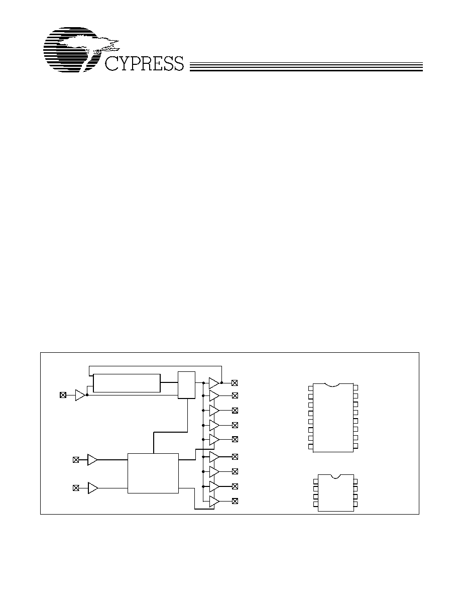
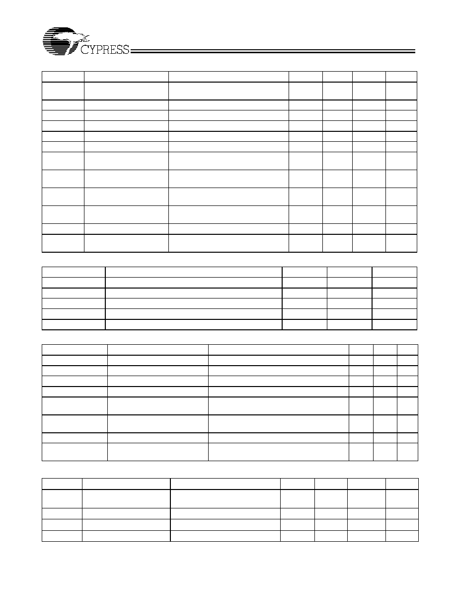
Block Diagram
1
2
3
4
5
6
7
8
9
10
11
12
13
14
15
16
REF
CLKA1
CLKA2
V
DD
GND
CLKB1
CLKB2
S2
CLKOUT
CLKA4
CLKA3
V
DD
GND
CLKB4
CLKB3
S1
SOIC/TSSOP
Top View
Pin Configuration
2309-1
2309-2
1
2
3
4
5
8
7
6
REF
CLK2
CLK1
GND
V
DD
CLKOUT
CLK4
CLK3
SOIC
Top View
2309-3
PLL
MUX
Select Input
REF
S2
S1
CLKA1
CLKA2
CLKA3
CLKA4
CLKB1
CLKB2
CLKB3
CLKB4
Decoding
CLKOUT
CY2305
CY2309
Document #: 38-07140 Rev. *C
Page 2 of 13
Notes:
1.
Weak pull-down.
2.
Weak pull-down on all outputs.
3.
Weak pull-ups on these inputs.
4.
This output is driven and has an internal feedback for the PLL. The load on this output can be adjusted to change the skew between the reference and output.
Pin Description for CY2309
Pin
Signal
Description
1
REF
[1]
Input reference frequency, 5V-tolerant input
2
CLKA1
[2]
Buffered clock output, Bank A
3
CLKA2
[2]
Buffered clock output, Bank A
4
V
DD
3.3V supply
5
GND
Ground
6
CLKB1
[2]
Buffered clock output, Bank B
7
CLKB2
[2]
Buffered clock output, Bank B
8
S2
[3]
Select input, bit 2
9
S1
[3]
Select input, bit 1
10
CLKB3
[2]
Buffered clock output, Bank B
11
CLKB4
[2]
Buffered clock output, Bank B
12
GND
Ground
13
V
DD
3.3V supply
14
CLKA3
[2]
Buffered clock output, Bank A
15
CLKA4
[2]
Buffered clock output, Bank A
16
CLKOUT
[2]
Buffered output, internal feedback on this pin
Pin Description for CY2305
Pin
Signal
Description
1
REF
[1]
Input reference frequency, 5V-tolerant input
2
CLK2
[2]
Buffered clock output
3
CLK1
[2]
Buffered clock output
4
GND
Ground
5
CLK3
[2]
Buffered clock output
6
V
DD
3.3V supply
7
CLK4
[2]
Buffered clock output
8
CLKOUT
[2]
Buffered clock output, internal feedback on this pin
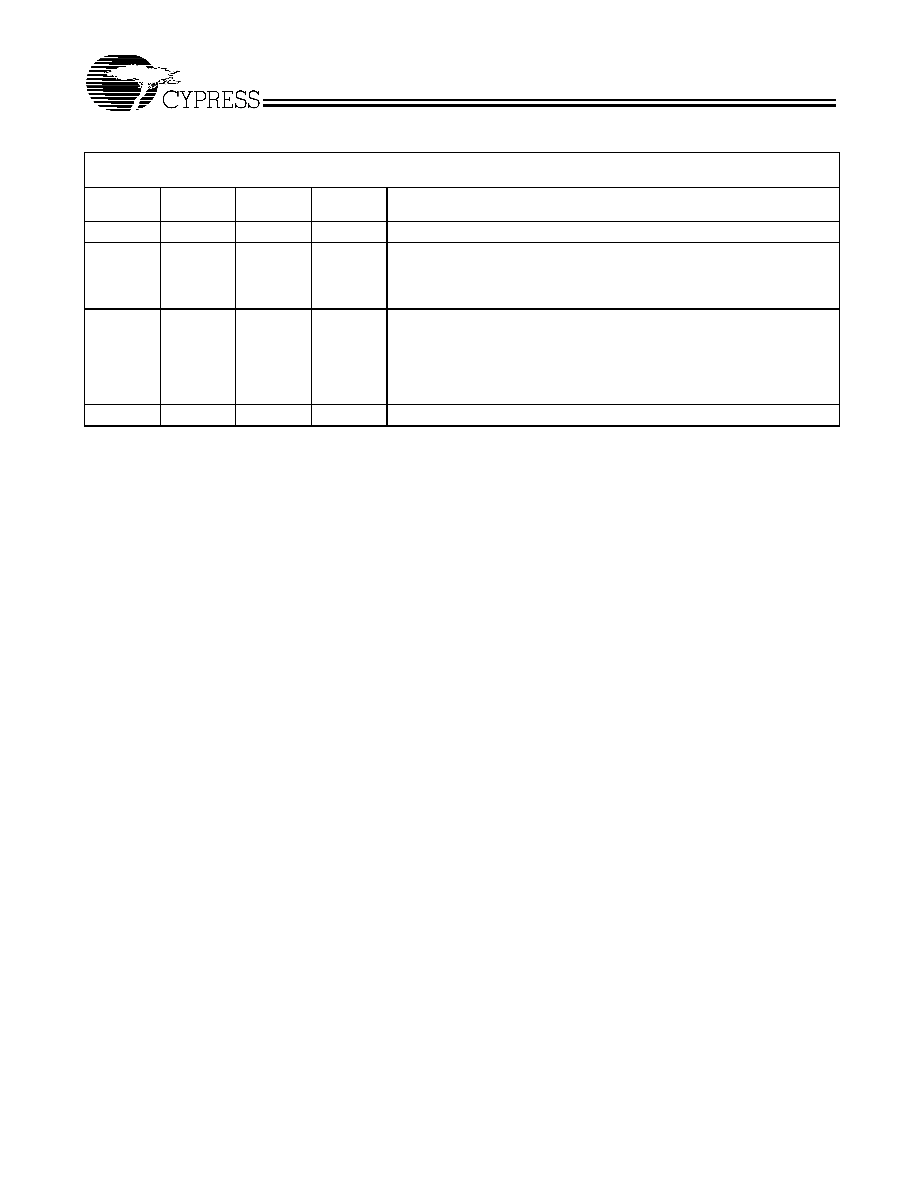
Select Input Decoding for CY2309
S2
S1
CLOCK A1≠A4
CLOCK B1≠B4
CLKOUT
[4]
Output Source
PLL Shutdown
0
0
Three-state
Three-state
Driven
PLL
N
0
1
Driven
Three-state
Driven
PLL
N
1
0
Driven
Driven
Driven
Reference
Y
1
1
Driven
Driven
Driven
PLL
N
CY2305
CY2309
Document #: 38-07140 Rev. *C
Page 3 of 13
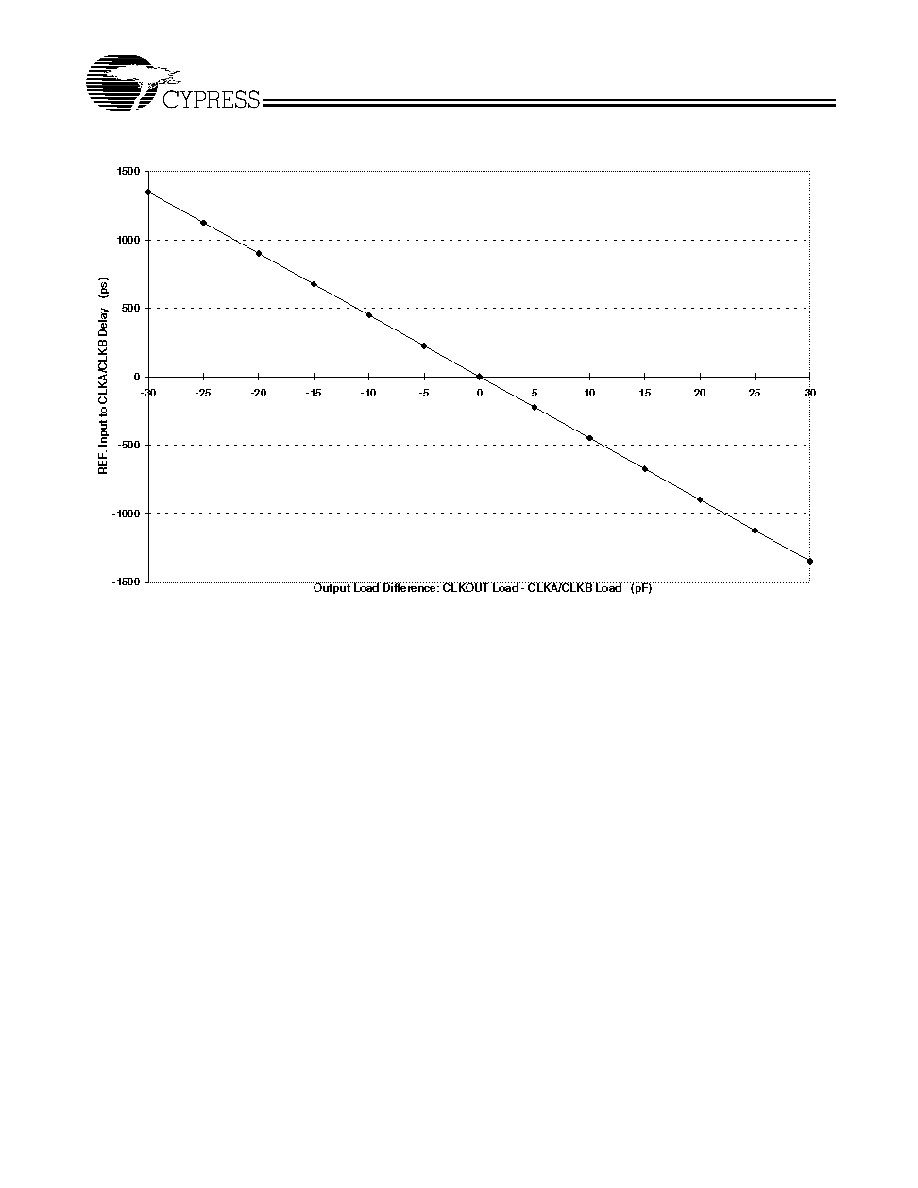
REF. Input to CLKA/CLKB Delay vs. Loading Difference between CLKOUT and CLKA/CLKB Pins
Zero Delay and Skew Control
All outputs should be uniformly loaded to achieve Zero Delay
between the input and output. Since the CLKOUT pin is the
internal feedback to the PLL, its relative loading can adjust the
input-output delay. This is shown in the above graph.
For applications requiring zero input-output delay, all outputs,
including CLKOUT, must be equally loaded. Even if CLKOUT
is not used, it must have a capacitive load, equal to that on
other outputs, for obtaining zero input-output delay. If input to
output delay adjustments are required, use the above graph to
calculate loading differences between the CLKOUT pin and
other outputs.
For zero output-output skew, be sure to load all outputs
equally. For further information refer to the application note
entitled "CY2305 and CY2309 as PCI and SDRAM Buffers."
CY2305
CY2309
Document #: 38-07140 Rev. *C
Page 4 of 13
Maximum Ratings
Supply Voltage to Ground Potential ............... ≠0.5V to +7.0V
DC Input Voltage (Except REF) ............≠0.5V to V
DD
+ 0.5V
DC Input Voltage REF......................................... ≠0.5V to 7V
Storage Temperature ................................. ≠65
∞
C to +150
∞
C
Junction Temperature ................................................. 150
∞
C
Static Discharge Voltage
(per MIL-STD-883, Method 3015) ........................... > 2,000V
Operating Conditions for CY2305SC-XX and CY2309SC-XX Commercial Temperature Devices
Parameter
Description
Min.
Max.
Unit
V
DD
Supply Voltage
3.0
3.6
V
T
A
Operating Temperature (Ambient Temperature)
0
70
∞
C
C
L
Load Capacitance, below 100 MHz
30
pF
C
L
Load Capacitance, from 100 MHz to 133 MHz
10
pF
C
IN
Input Capacitance
7
pF
t
PU
Power-up time for all VDD's to reach minimum specified voltage
(power ramps must be monotonic)
0.05
50
ms
Electrical Characteristics for CY2305SC-XX and CY2309SC-XX Commercial Temperature Devices
Parameter
Description
Test Conditions
Min.
Max.
Unit
V
IL
Input LOW Voltage
[5]
0.8
V
V
IH
Input HIGH Voltage
[5]
2.0
V
I
IL
Input LOW Current
V
IN
= 0V
50.0
µ
A
I
IH
Input HIGH Current
V
IN
= V
DD
100.0
µ
A
V
OL
Output LOW Voltage
[6]
I
OL
= 8 mA (≠1)
I
OH =
12
mA (≠1H)
0.4
V
V
OH
Output HIGH Voltage
[6]
I
OH
= ≠8 mA (≠1)
I
OL
= ≠12 mA (≠1H)
2.4
V
I
DD
(PD mode)
Power Down Supply Current
REF = 0 MHz
12.0
µ
A
I
DD
Supply Current
Unloaded outputs at 66.67 MHz,
SEL inputs at V
DD
32.0
mA
Switching Characteristics for CY2305SC-1and CY2309SC-1 Commercial Temperature Devices
[7]
Parameter
Name
Test Conditions
Min.
Typ.
Max.
Unit
t1
Output Frequency
30-pF load
10-pF load
10
10
100
133.33
MHz
MHz
Duty Cycle
[6]
= t
2
˜
t
1
Measured at 1.4V, F
out
= 66.67 MHz
40.0
50.0
60.0
%
t3
Rise Time
[6]
Measured between 0.8V and 2.0V
2.50
ns
t
4
Fall Time
[6]
Measured between 0.8V and 2.0V
2.50
ns
t
5
Output to Output Skew
[6]
All outputs equally loaded
250
ps
t
6A
Delay, REF Rising Edge to
CLKOUT Rising Edge
[6]
Measured at V
DD
/2
0
±350
ps
t
6B
Delay, REF Rising Edge to
CLKOUT Rising Edge
[6]
Measured at V
DD
/2. Measured in PLL
Bypass Mode, CY2309 device only.
1
5
8.7
ns
t
7
Device to Device Skew
[6]
Measured at V
DD
/2 on the CLKOUT pins
of devices
0
700
ps
t
J
Cycle to Cycle Jitter
[6]
Measured at 66.67 MHz, loaded outputs
200
ps
t
LOCK
PLL Lock Time
[6]
Stable power supply, valid clock
presented on REF pin
1.0
ms
Notes:
5.
REF input has a threshold voltage of V
DD
/2.
6.
Parameter is guaranteed by design and characterization. Not 100% tested in production.
7.
All parameters specified with loaded outputs.
CY2305
CY2309
Document #: 38-07140 Rev. *C
Page 5 of 13
Switching Characteristics for CY2305SC-1H and CY2309SC-1H Commercial Temperature Devices
[7]
Parameter
Name
Description
Min.
Typ.
Max.
Unit
t1
Output Frequency
30-pF load
10-pF load
10
10
100
133.33
MHz
MHz
Duty Cycle
[6]
= t
2
˜
t
1
Measured at 1.4V, F
out
= 66.67 MHz
40.0
50.0
60.0
%
Duty Cycle
[6]
= t
2
˜
t
1
Measured at 1.4V, F
out
<50.0 MHz
45.0
50.0
55.0
%
t3
Rise Time
[6]
Measured between 0.8V and 2.0V
1.50
ns
t
4
Fall Time
[6]
Measured between 0.8V and 2.0V
1.50
ns
t
5
Output to Output Skew
[6]
All outputs equally loaded
250
ps
t
6A
Delay, REF Rising Edge to
CLKOUT Rising Edge
[6]
Measured at V
DD
/2
0
±350
ps
t
6B
Delay, REF Rising Edge to
CLKOUT Rising Edge
[6]
Measured at V
DD
/2. Measured in PLL
Bypass Mode, CY2309 device only.
1
5
8.7
ns
t
7
Device to Device Skew
[6]
Measured at V
DD
/2 on the CLKOUT pins
of devices
0
700
ps
t
8
Output Slew Rate
[6]
Measured between 0.8V and 2.0V using
Test Circuit #2
1
V/ns
t
J
Cycle to Cycle Jitter
[6]
Measured at 66.67 MHz, loaded outputs
200
ps
t
LOCK
PLL Lock Time
[6]
Stable power supply, valid clock
presented on REF pin
1.0
ms
Operating Conditions for CY2305SI-XX and CY2309SI-XX Industrial Temperature Devices
Parameter
Description
Min.
Max.
Unit
V
DD
Supply Voltage
3.0
3.6
V
T
A
Operating Temperature (Ambient Temperature)
≠40
85
∞
C
C
L
Load Capacitance, below 100 MHz
30
pF
C
L
Load Capacitance, from 100 MHz to 133 MHz
10
pF
C
IN
Input Capacitance
7
pF
Electrical Characteristics for CY2305SI-XX and CY2309SI-XX Industrial Temperature Devices
Parameter
Description
Test Conditions
Min.
Max.
Unit
V
IL
Input LOW Voltage
[5]
0.8
V
V
IH
Input HIGH Voltage
[5]
2.0
V
I
IL
Input LOW Current
V
IN
= 0V
50.0
µ
A
I
IH
Input HIGH Current
V
IN
= V
DD
100.0
µ
A
V
OL
Output LOW Voltage
[6]
I
OL
= 8 mA (-1)
I
OH
=12
mA (-1H)
0.4
V
V
OH
Output HIGH Voltage
[6]
I
OH
= ≠8 mA (-1)
I
OL
= ≠12 mA (-1H)
2.4
V
I
DD
(PD mode)
Power Down Supply Current
REF = 0 MHz
25.0
µ
A
I
DD
Supply Current
Unloaded outputs at 66.67 MHz, SEL inputs at
V
DD
35.0
mA
Switching Characteristics for CY2305SI-1and CY2309SI-1 Industrial Temperature Devices
[7]
Parameter
Name
Test Conditions
Min.
Typ.
Max.
Unit
t1
Output Frequency
30-pF load
10-pF load
10
10
100
133.33
MHz
MHz
Duty Cycle
[6]
= t
2
˜
t
1
Measured at 1.4V, F
out
= 66.67 MHz
40.0
50.0
60.0
%
t3
Rise Time
[6]
Measured between 0.8V and 2.0V
2.50
ns
t
4
Fall Time
[6]
Measured between 0.8V and 2.0V
2.50
ns
CY2305
CY2309
Document #: 38-07140 Rev. *C
Page 6 of 13
t
5
Output to Output Skew
[6]
All outputs equally loaded
250
ps
t
6A
Delay, REF Rising Edge to
CLKOUT Rising Edge
[6]
Measured at V
DD
/2
0
±350
ps
t
6B
Delay, REF Rising Edge to
CLKOUT Rising Edge
[6]
Measured at V
DD
/2. Measured in
PLL Bypass Mode, CY2309 device
only.
1
5
8.7
ns
t
7
Device to Device Skew
[6]
Measured at V
DD
/2 on the CLKOUT
pins of devices
0
700
ps
t
J
Cycle to Cycle Jitter
[6]
Measured at 66.67 MHz, loaded
outputs
200
ps
t
LOCK
PLL Lock Time
[6]
Stable power supply, valid clock
presented on REF pin
1.0
ms
Switching Characteristics for CY2305SI-1H and CY2309SI-1H Industrial Temperature Devices
[7]
Parameter
Name
Description
Min.
Typ.
Max.
Unit
t
1
Output Frequency
30-pF load
10-pF load
10
10
100
133.33
MHz
MHz
Duty Cycle
[6]
= t
2
˜
t
1
Measured at 1.4V, F
out
= 66.67 MHz
40.0
50.0
60.0
%
Duty Cycle
[6]
= t
2
˜
t
1
Measured at 1.4V, F
out
< 50.0 MHz
45.0
50.0
55.0
%
t
3
Rise Time
[6]
Measured between 0.8V and 2.0V
1.50
ns
t
4
Fall Time
[6]
Measured between 0.8V and 2.0V
1.50
ns
t
5
Output to Output Skew
[6]
All outputs equally loaded
250
ps
t
6A
Delay, REF Rising Edge to
CLKOUT Rising Edge
[6]
Measured at V
DD
/2
0
±350
ps
t
6B
Delay, REF Rising Edge to
CLKOUT Rising Edge
[6]
Measured at V
DD
/2. Measured in
PLL Bypass Mode, CY2309 device
only.
1
5
8.7
ns
t
7
Device to Device Skew
[6]
Measured at V
DD
/2 on the CLKOUT
pins of devices
0
700
ps
t
8
Output Slew Rate
[6]
Measured between 0.8V and 2.0V
using Test Circuit #2
1
V/ns
t
J
Cycle to Cycle Jitter
[6]
Measured at 66.67 MHz, loaded
outputs
200
ps
t
LOCK
PLL Lock Time
[6]
Stable power supply, valid clock
presented on REF pin
1.0
ms
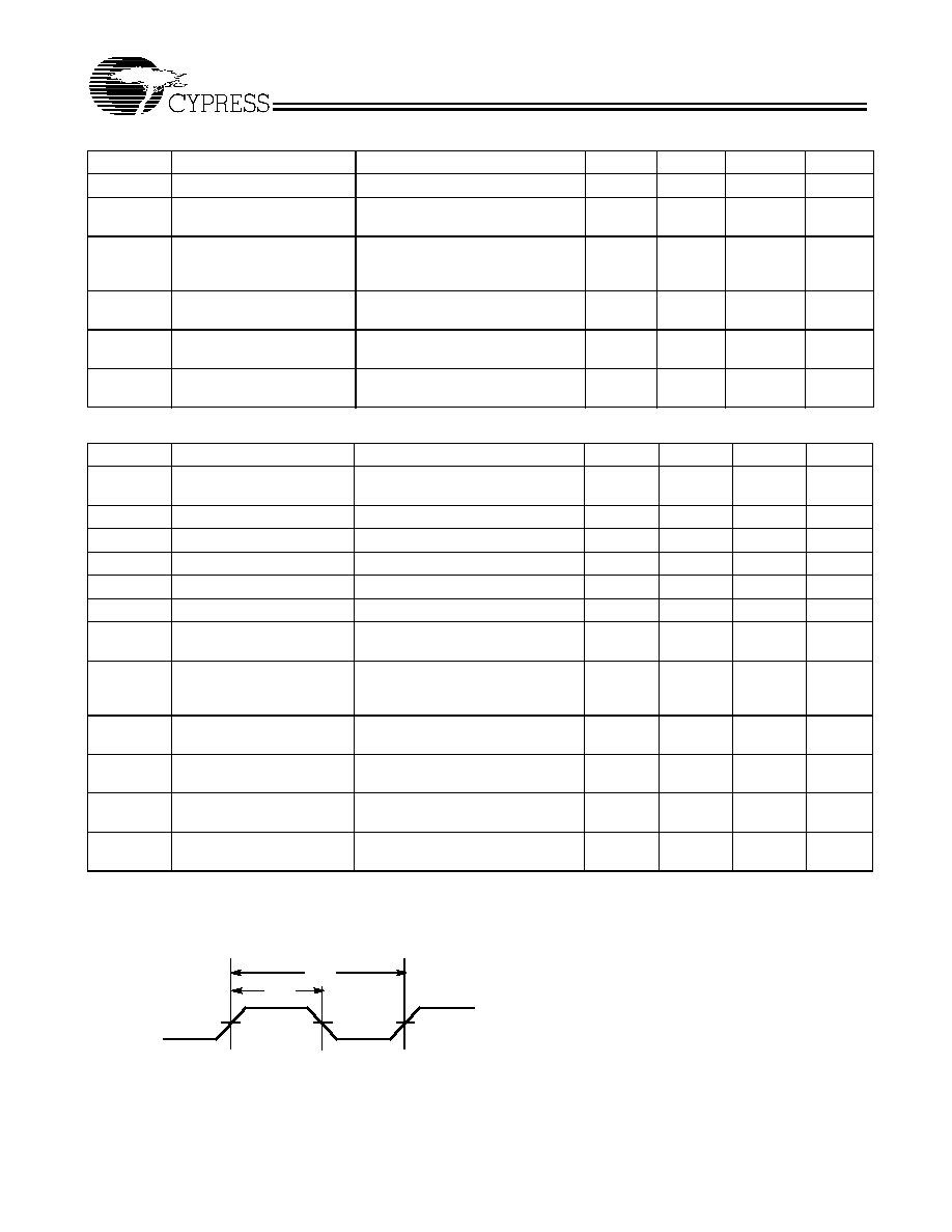
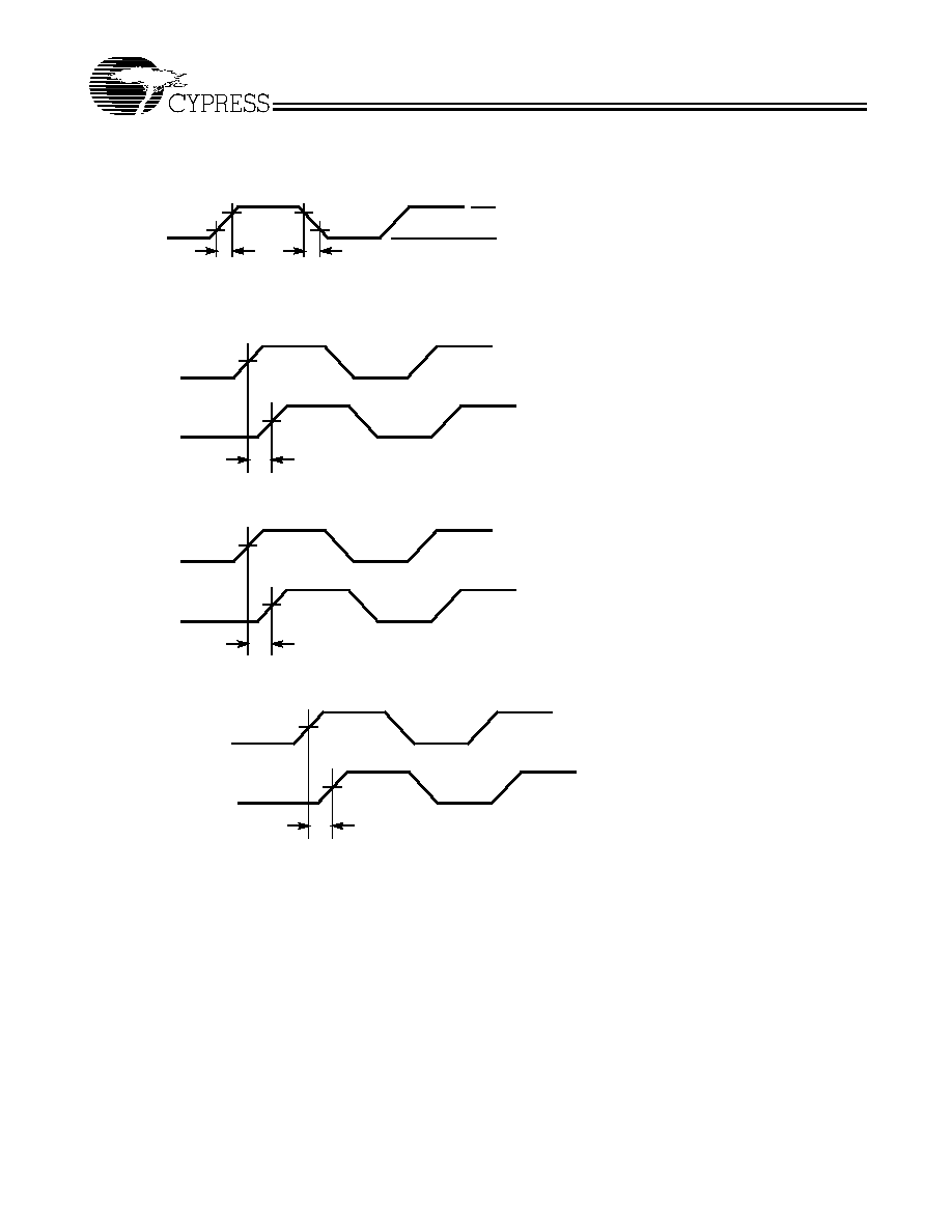
Switching Waveforms
Switching Characteristics for CY2305SI-1and CY2309SI-1 Industrial Temperature Devices
[7]
Parameter
Name
Test Conditions
Min.
Typ.
Max.
Unit
Duty Cycle Timing
t
1
t
2
1.4V
1.4V
1.4V
CY2305
CY2309
Document #: 38-07140 Rev. *C
Page 7 of 13
Switching Waveforms
(continued)
All Outputs Rise/Fall Time
OUTPUT
t
3
3.3V
0V
0.8V
2.0V
2.0V
0.8V
t
4
Output-Output Skew
1.4V
1.4V
t
5
OUTPUT
OUTPUT
Input-Output Propagation Delay
V
DD
/2
t
6
INPUT
OUTPUT
V
DD
/2
V
DD
/2
V
DD
/2
t
7
CLKOUT, Device 1
CLKOUT, Device 2
Device-Device Skew
CY2305
CY2309
Document #: 38-07140 Rev. *C
Page 8 of 13
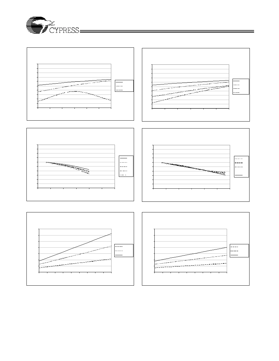
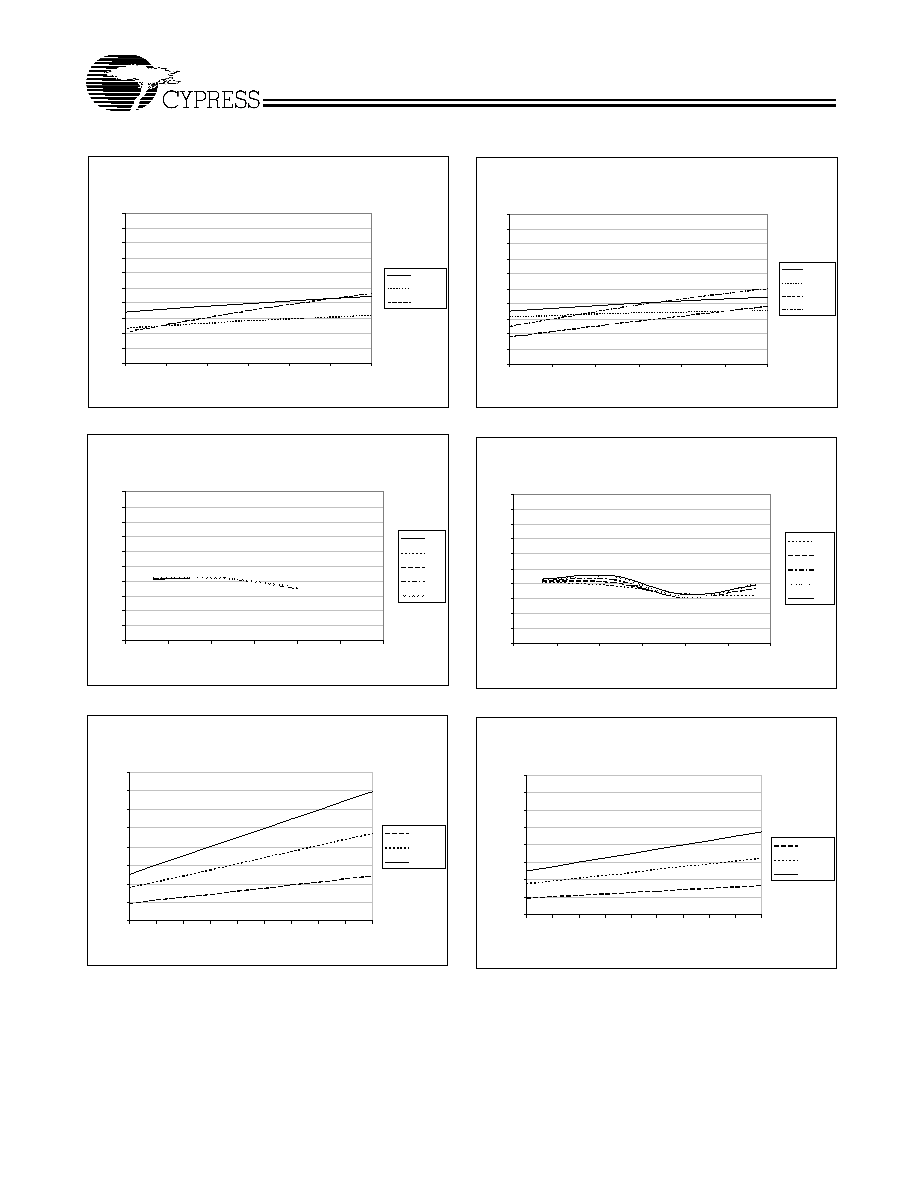
Typical Duty Cycle
[8]
and I
DD
Trends
[9]
for CY2305-1 and CY2309-1
Notes:
8.
Duty Cycle is taken from typical chip measured at 1.4V.
9.
I
DD
data is calculated from I
DD
= I
CORE
+ nCVf, where I
CORE
is the unloaded current. (n = # of outputs; C = Capacitance load per output (F); V = Supply
Voltage (V); f = frequency (Hz)).
Duty Cycle Vs VDD
(for 30 pF Loads over Frequency - 3.3V, 25C)
40
42
44
46
48
50
52
54
56
58
60
3
3.1
3.2
3.3
3.4
3.5
3.6
VDD (V)
Du
t
y
Cy
c
l
e
(
%
)
33 MHz
66 MHz
100 MHz
Duty Cycle Vs VDD
(for 15 pF Loads over Frequency - 3.3V, 25C)
40
42
44
46
48
50
52
54
56
58
60
3
3.1
3.2
3.3
3.4
3.5
3.6
VDD (V)
Du
ty
Cy
c
l
e
(
%
)
33 MHz
66 MHz
100 MHz
133 MHz
Duty Cycle Vs Frequency
(for 30 pF Loads over Temperature - 3.3V)
40
42
44
46
48
50
52
54
56
58
60
20
40
60
80
100
120
140
Frequency (MHz)
Du
t
y
C
y
c
l
e
(
%
)
-40C
0C
25C
70C
85C
Duty Cycle Vs Frequency
(for 15 pF Loads over Temperature - 3.3V)
40
42
44
46
48
50
52
54
56
58
60
20
40
60
80
100
120
140
Fre quency (MHz)
Du
t
y
Cy
cle
(
%
)
-40C
0C
25C
70C
85C
IDD vs Number of Loaded Outputs
(for 30 pF Loads over Frequency - 3.3V, 25C)
0
20
40
60
80
100
120
140
0
1
2
3
4
5
6
7
8
9
# of Loaded Outputs
IDD (
m
A)
33 MHz
66 MHz
100 MHz
IDD vs Number of Loaded Outputs
(for 15 pF Loads over Frequency - 3.3V, 25C)
0
20
40
60
80
100
120
140
0
1
2
3
4
5
6
7
8
9
# of Loaded Outputs
IDD (
m
A)
33 MHz
66 MHz
100 MHz
CY2305
CY2309
Document #: 38-07140 Rev. *C
Page 9 of 13
Typical Duty Cycle
[8]
and IDD Trends
[9]
for CY2305-1H and CY2309-1H
Duty Cycle Vs VDD
(for 30 pF Loads over Frequency - 3.3V, 25C)
40
42
44
46
48
50
52
54
56
58
60
3
3.1
3.2
3.3
3.4
3.5
3.6
VDD (V)
Du
t
y
Cy
c
l
e
(
%
)
33 MHz
66 MHz
100 MHz
Duty Cycle Vs VDD
(for 15 pF Loads over Frequency - 3.3V, 25C)
40
42
44
46
48
50
52
54
56
58
60
3
3.1
3.2
3.3
3.4
3.5
3.6
VDD (V)
Du
t
y
Cy
c
l
e
(
%
)
33 MHz
66 MHz
100 MHz
133 MHz
Duty Cycle Vs Frequency
(for 30 pF Loads over Temperature - 3.3V)
40
42
44
46
48
50
52
54
56
58
60
20
40
60
80
100
120
140
Frequency (MHz)
Du
t
y
Cy
c
l
e
(
%
)
-40C
0C
25C
70C
85C
Duty Cycle Vs Frequency
(for 15 pF Loads over Temperature - 3.3V)
40
42
44
46
48
50
52
54
56
58
60
20
40
60
80
100
120
140
Frequency (MHz)
Du
t
y
Cy
c
l
e
(
%
)
-40C
0C
25C
70C
85C
IDD vs Number of Loaded Outputs
(for 30 pF Loads over Frequency - 3.3V, 25C)
0
20
40
60
80
100
120
140
160
0
1
2
3
4
5
6
7
8
9
# of Loaded Outputs
IDD (
m
A)
33 MHz
66 MHz
100 MHz
IDD vs Number of Loaded Outputs
(for 15 pF Loads over Frequency - 3.3V, 25C)
0
20
40
60
80
100
120
140
160
0
1
2
3
4
5
6
7
8
9
# of Loaded Outputs
IDD (
m
A)
33 MHz
66 MHz
100 MHz
CY2305
CY2309
Document #: 38-07140 Rev. *C
Page 10 of 13
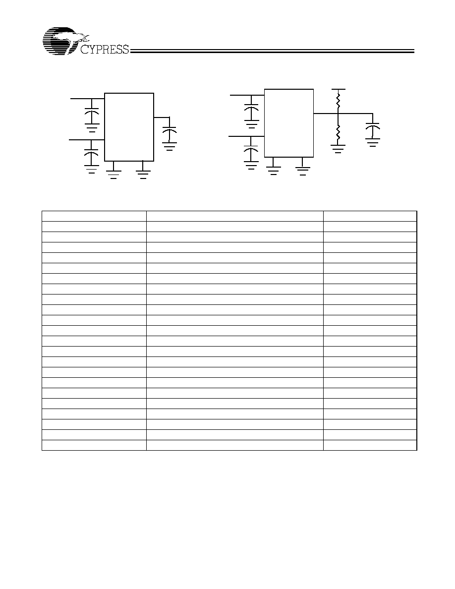
Test Circuits
Ordering Information
Ordering Code
Package Type
Operating Range
CY2305SC-1
8-pin 150-mil SOIC
Commercial
CY2305SC-1T
8-pin 150-mil SOIC≠Tape and Reel
Commercial
CY2305SI-1
8-pin 150-mil SOIC
Industrial
CY2305SI-1T
8-pin 150-mil SOIC≠Tape and Reel
Industrial
CY2305SC-1H
8-pin 150-mil SOIC
Commercial
CY2305SC-1HT
8-pin 150-mil SOIC≠Tape and Reel
Commercial
CY2305SI-1H
8-pin 150-mil SOIC
Industrial
CY2305SI-1HT
8-pin 150-mil SOIC≠Tape and Reel
Industrial
CY2305ZC-1
8-pin 150-mil TSSOP
Commercial
CY2305ZC-1T
8-pin 150-mil TSSOP≠Tape and Reel
Commercial
CY2309SC-1
16-pin 150-mil SOIC
Commercial
CY2309SC-1T
16-pin 150-mil SOIC≠Tape and Reel
Commercial
CY2309SI-1
16-pin 150-mil SOIC
Industrial
CY2309SI-1T
16-pin 150-mil SOIC≠Tape and Reel
Industrial
CY2309SC-1H
16-pin 150-mil SOIC
Commercial
CY2309SC-1HT
16-pin 150-mil SOIC≠Tape and Reel
Commercial
CY2309SI-1H
16-pin 150-mil SOIC
Industrial
CY2309SI-1HT
16-pin 150-mil SOIC≠Tape and Reel
Industrial
CY2309ZC-1H
16-pin 4.4-mm TSSOP
Commercial
CY2309ZC-1HT
16-pin 4.4-mm TSSOP≠Tape and Reel
Commercial
CY2309ZI-1H
16-pin 4.4-mm TSSOP
Industrial
CY2309ZI-1HT
16-pin 4.4-mm TSSOP≠Tape and Reel
Industrial
0.1
µ
F
V DD
0.1
µ
F
V DD
CLK
out
C LOAD
OUTPUTS
GND
GND
0.1
µ
F
V DD
0.1
µ
F
V DD
10 pF
OUTPUTS
GND
GND
1 k
1 k
Test Circuit # 1
Test Circuit # 2
For parameter t
8
(output slew rate) on -1H devices
CY2305
CY2309
Document #: 38-07140 Rev. *C
Page 11 of 13
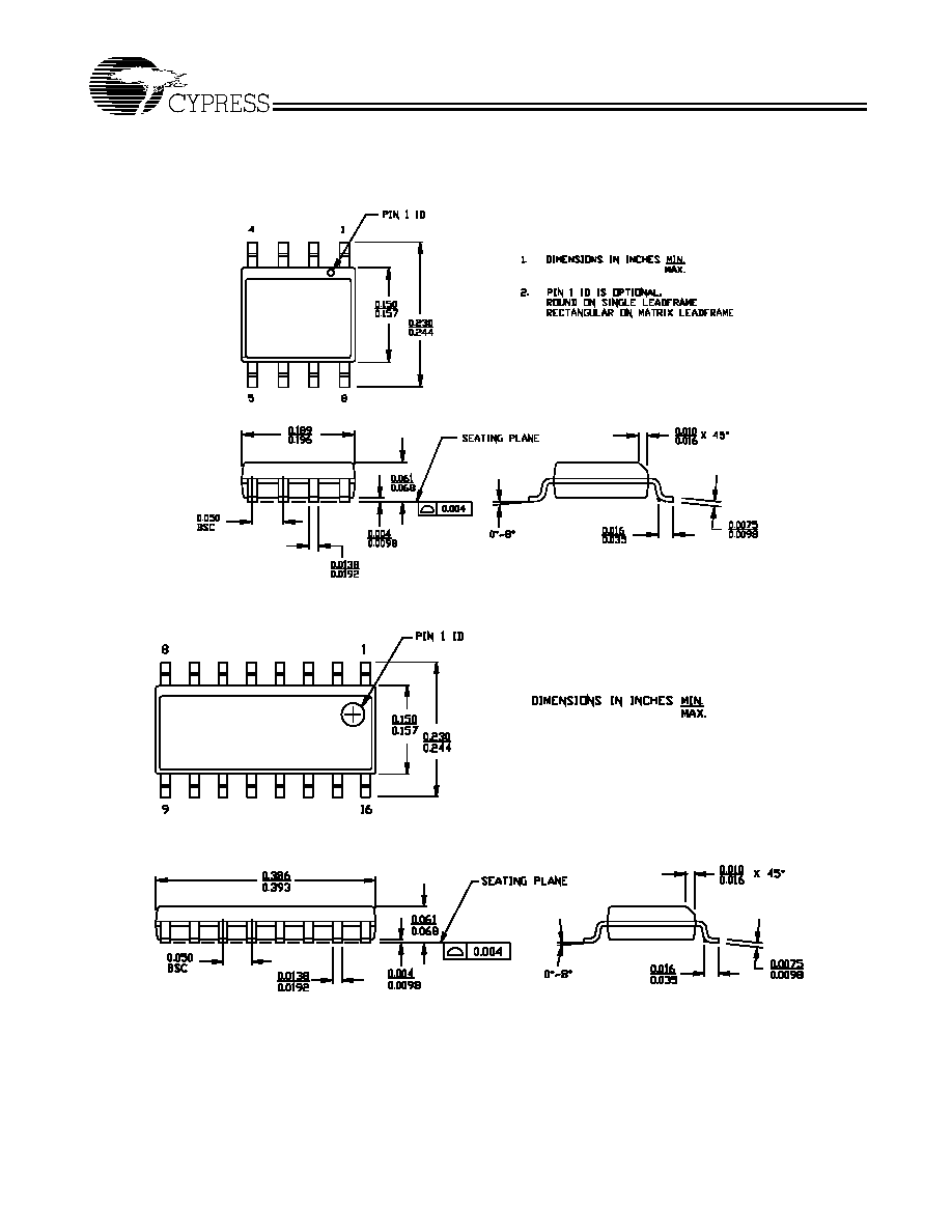
Package Diagrams
8-lead (150-Mil) SOIC S8
51-85066-A
16-lead (150-Mil) Molded SOIC S16
51-85068-A
CY2305
CY2309
Document #: 38-07140 Rev. *C
Page 12 of 13
© Cypress Semiconductor Corporation, 2002. The information contained herein is subject to change without notice. Cypress Semiconductor Corporation assumes no responsibility for the use
of any circuitry other than circuitry embodied in a Cypress Semiconductor product. Nor does it convey or imply any license under patent or other rights. Cypress Semiconductor does not authorize
its products for use as critical components in life-support systems where a malfunction or failure may reasonably be expected to result in significant injury to the user. The inclusion of Cypress
Semiconductor products in life-support systems application implies that the manufacturer assumes all risk of such use and in doing so indemnifies Cypress Semiconductor against all charges.
Pentium is a registered trademark of Intel Corporation. All product and company names mentioned in this document may be the
trademarks of their respective holders.
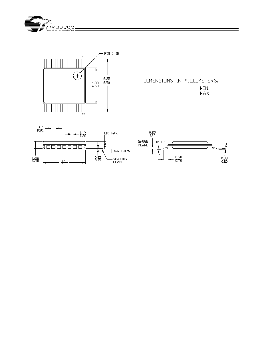
Package Diagrams
(continued)
16-lead Thin Shrunk Small Outline Package (4.40 MM Body) Z16
51-85091-**
CY2305
CY2309
Document #: 38-07140 Rev. *C
Page 13 of 13
Document History Page
Document Title: CY2305/CY2309 Low-Cost 3.3V Zero Delay Buffer
Document Number: 38-07140
REV.
ECN NO.
Issue Date
Orig. of
Change
Description of Change
**
110249
10/19/01
SZV
Change from Spec number: 38-00530 to 38-07140
*A
111117
03/01/02
CKN
Added t6B row to the Switching Characteristics Table; also added the letter
"A" to the t6A row
Corrected the table title from CY2305SC-IH and CY2309SC-IH to
CY2305SI-IH and CY2309SI-IH
*B
117625
10/21/02
HWT
Added eight-pin TSSOP packages (CY2305ZC-1 and CY2305ZC-1T) to the
ordering information table.
Added the Tape and Reel option to all the existing packages:
CY2305SC-1T, CY2305SI-1T, CY2305SC-1HT, CY2305SI-1HT,
CY2305ZC-1T, CY2309SC-1T, CY2309SI-1T, CY2309SC-1HT,
CY2309SI-1HT, CY2309ZC-1HT, CY2309ZI-1HT
*C
121828
12/14/02
RBI
Power up requirements added to Operating Conditions Information