3.3V SDRAM Buffer for Mobile PCs
with Four SO-DIMMs
CY2310BNZ
Cypress Semiconductor Corporation
∑
3901 North First Street
∑
San Jose
,
CA 95134
∑
408-943-2600
Document #: 38-07260 Rev. *A
Revised January 28, 2003
Features
∑ One input to 10 output buffer/driver
∑ Supports up to four SDRAM SO-DIMMs
∑ Two additional outputs for feedback
∑ SMBus interface for output control
∑ Low skew outputs
∑ Up to 100 MHz operation
∑ Multiple V
DD
and V
SS
pins for noise reduction
∑ Dedicated OE pin for testing
∑ Space-saving 28-pin SSOP package
∑ 3.3V operation
Description
The CY2310BNZ is a 3.3V buffer designed to distribute
high-speed clocks in mobile PC applications. The part has ten
outputs, eight of which can be used to drive up to four SDRAM
SO-DIMMs, and the remaining can be used for external
feedback to a PLL. The device operates at 3.3V and outputs
can run up to 100 MHz, thus making it compatible with
Pentium II
processors. The CY2310BNZ can be used in
conjunction with the CY2281 or similar clock synthesizer for a
full Pentium II motherboard solution.
The CY2310BNZ also includes an SMBus interface that can
enable or disable each output clock. On power-up, all output
clocks are enabled. A separate Output Enable pin facilitates
testing on ATE.
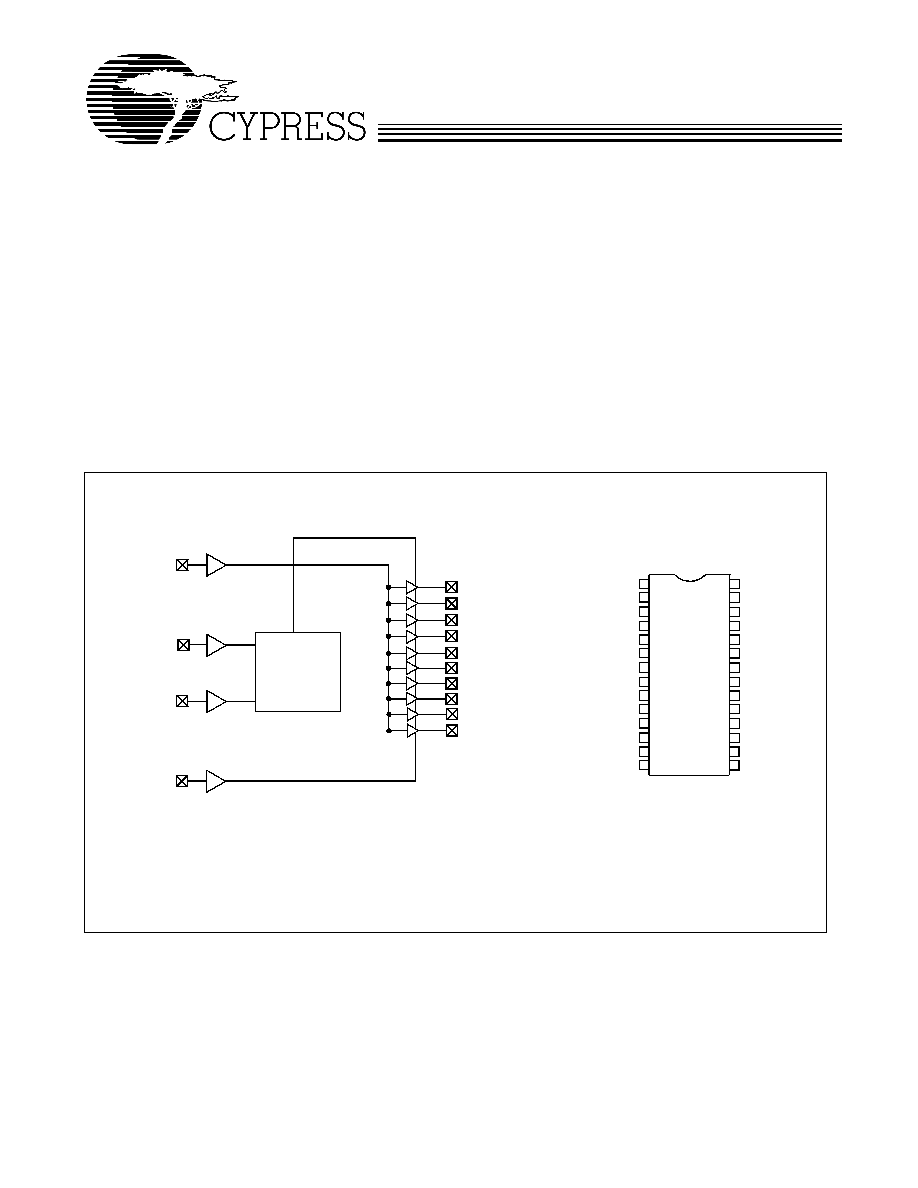
Block Diagram
SMBus
BUF_IN
SDATA
SCLOCK
SDRAM0
SDRAM1
SDRAM2
SDRAM3
SDRAM4
SDRAM5
SDRAM6
SDRAM7
1
2
3
4
V
DD
SDRAM7
SDRAM6
V
SS
V
DD
SDRAM5
28-pin SSOP
Top View
Pin Configuration
Decoding
8
5
6
7
12
9
10
11
13
14
28
27
26
25
21
24
23
22
17
20
19
18
16
15
SDRAM4
V
SS
OE
V
DD
SDRAM9
V
SS
V
SSIIC
SCLOCK
V
DD
SDRAM0
SDRAM1
V
SS
V
DD
SDRAM2
V
SS
BUF_IN
V
DD
SDRAM8
V
SS
V
DDIIC
SDATA
SDRAM3
SDRAM8
SDRAM9
OE
CY2
3
1
0
BNZ
CY2310BNZ
Document #: 38-07260 Rev. *A
Page 2 of 6
Device Functionality
Serial Configuration Map
∑ The Serial bits will be read by the clock driver in the following
order:
Byte 0 - Bits 7, 6, 5, 4, 3, 2, 1, 0
Byte 1 - Bits 7, 6, 5, 4, 3, 2, 1, 0
.
Byte N - Bits 7, 6, 5, 4, 3, 2, 1, 0
∑ Reserved and unused bits should be programmed to "0."
∑ SMBus Address for the CY2310BNZ is:
Pin Description
Pins
Name
Description
1, 5, 10, 19, 24, 28
V
DD
3.3V Digital voltage supply
4, 8, 12, 17, 21, 25
V
SS
Ground
13
V
DDIIC
SMBus Voltage supply
16
V
SSIIC
Ground for SMBus
9
BUF_IN
Input clock
20
OE
Output Enable, three-states outputs when LOW. Internal pull-up to V
DD
14
SDATA
SMBus data input, internal pull-up to V
DD
15
SCLK
SMBus clock input, internal pull-up to V
DD
2, 3, 6, 7
SDRAM [0≠3]
SDRAM byte 0 clock outputs
22, 23, 26, 27
SDRAM [4≠7]
SDRAM byte 1 clock outputs
11, 18
SDRAM [8≠9]
SDRAM byte 2 clock outputs
OE
SDRAM [0≠17]
0
High-Z
1
1 x BUF_IN
A6
A5
A4
A3
A2
A1
A0
R/W
1
1
0
1
0
0
1
----
Byte 0:SDRAM Active/Inactive Register
(1 = Enable, 0 = Disable), Default = Enabled
Bit
Pin #
Description
Bit 7 ≠
Initialize to 0
Bit 6 ≠
Initialize to 0
Bit 5 ≠
Initialize to 0
Bit 4 ≠
Initialize to 0
Bit 3 7
SDRAM3 (Active/Inactive)
Bit 2 6
SDRAM2 (Active/Inactive)
Bit 1 3
SDRAM1 (Active/Inactive)
Bit 0 2
SDRAM0 (Active/Inactive)
Byte 1: SDRAM Active/Inactive Register
(1 = Active, 0 = Inactive), Default = Active
Bit
Pin #
Description
Bit 7
27
SDRAM7 (Active/Inactive)
Bit 6
26
SDRAM6 (Active/Inactive)
Bit 5
23
SDRAM5 (Active/Inactive)
Bit 4
22
SDRAM4 (Active/Inactive)
Bit 3
≠
Initialize to 0
Bit 2
≠
Initialize to 0
Bit 1
≠
Initialize to 0
Bit 0
≠
Initialize to 0
Byte 2: SDRAM Active/Inactive Register
(1 = Active, 0 = Inactive), Default = Active
Bit
Pin #
Description
Bit 7
18
SDRAM9 (Active/Inactive)
Bit 6
11
SDRAM8 (Active/Inactive)
Bit 5
≠
Reserved, drive to 0
Bit 4
≠
Reserved, drive to 0
Bit 3
≠
Reserved, drive to 0
Bit 2
≠
Reserved, drive to 0
Bit 1
≠
Reserved, drive to 0
Bit 0
≠
Reserved, drive to 0
CY2310BNZ
Document #: 38-07260 Rev. *A
Page 3 of 6
Absolute Maximum Conditions
Parameter
Description
Condition
Min.
Max.
Unit
V
DD
Core Supply Voltage
≠0.5
7.0
V
V
IN
Input Voltage
Relative to V
SS
≠0.5
V
DD
+0.5
VDC
T
S
Temperature, Storage
Non Functional
≠65
+150
∞C
T
A
Temperature, Operating Ambient
Functional
≠40
85
∞C
T
J
Temperature, Junction
Functional
150
∞C
ÿ
JC
Dissipation, Junction to Case
Mil-Spec 883E Method 1012.1
32.24
∞C/W
ÿ
JA
Dissipation, Junction to Ambient
JEDEC (JESD 51)
98.31
∞C/W
ESD
HBM
ESD Protection (Human Body Model)
MIL-STD-883, Method 3015
2000
Volts
UL≠94
Flammability Rating
@1/8 in.
V≠0
MSL
Moisture Sensitivity Level
1
ppm
DC Electrical Specifications
Parameter
Description
Condition
Min.
Max.
Unit
V
DD
Supply Voltage
@3.3V± 5%
3.135
3.465
V
I
DD1
3.3V Supply Current
at 64MHz
100
180
mA
I
DD2
3.3V Supply Current
at 100 MHz
150
220
mA
I
DD Tristate
3.3V Supply Current in
Three-State
≠
10
mA
Logic Inputs
V
IL
Input Low Voltage
V
SS
≠0.3
0.8
V
V
IH
Input High Voltage
2.0
V
DD
+0.5
V
I
IL1
Input Leakage Current, BUF_IN
≠5
+5
µA
I
IL2
Input Leakage Current
[1]
≠20
+5
µA
Logic Outputs (SDRAM0:9)
[2]
V
OL
Output Low Voltage
I
OL
= 1 mA
≠
50
mV
V
OH
Output High Voltage
I
OH
= ≠1 mA
3.1
≠
V
I
OL
Output Low Current
V
OL
= 1.5V
70
185
mA
I
OH
Output High Current
V
OH
= 1.5V
65
160
mA
Pin Capacitance/Inductance
C
IN
Input Pin Capacitance
≠
5
pF
C
OUT
Output Pin Capacitance
≠
6
pF
L
IN
Input Pin Inductance
≠
7
nH
C
LOAD
Input Load Capacitance
20
30
pF
AC Electrical Specifications
Parameter
Description
Test Condition
Min.
Max.
Unit
F
IN
Input Frequency
at 64 MHz
0
133
MHz
T
R
Output Rise Edge Rate
Measured from 0.4V to 2.4V
1.5
4.0
V/ns
T
F
Output Fall Edge Rate
Measured from 2.4V to 0.4V
1.5
4.0
V/ns
T
SR
Output Skew, Rising Edges
200
ps
T
SF
Output Skew, Falling Edges
200
ps
T
EN
Output Enable Time
1.0
8.0
ns
T
DIS
Output Disable Time
1.0
8.0
ns
Notes:
1.
OE, SDATA, and SCLOCK logic pins have a 250-k
internal pull-up resistor (V
DD
≠ 0.8V).
2.
All SDRAM outputs loaded by 6" transmission lines with 22-pF capacitors on ends.
CY2310BNZ
Document #: 38-07260 Rev. *A
Page 4 of 6
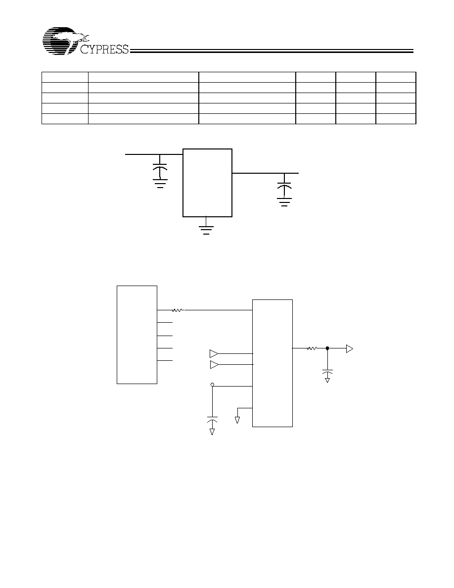
Test Circuit
Application Information
Clock traces must be terminated with either series or parallel
termination, as they are normally done.
Summary
∑ Surface mount, low-ESR ceramic capacitors should be
used for filtering. Typically, these capacitors have a value
of 0.1
µ
F. In some cases, smaller value capacitors may be
required.
∑ The value of the series-terminating resistor satisfies the
following equation where Rtrace is the loaded characteristic
impedance of the trace, Rout is the output impedance of the
buffer (typically 25W), and Rseries is the series terminating
resistor.
Rseries > Rtrace ≠ Rout
∑ Footprints must be laid out for optional EMI-reducing capac-
itors, which should be placed as close to the terminating
resistor as is physically possible. Typical values of these
capacitors range from 4.7 pF to 22 pF.
∑ A Ferrite Bead may be used to isolate the Board V
DD
from
the clock generator V
DD
island. Ensure that the Ferrite Bead
t
PR
Rising Edge Propagation Delay
3.0
5.0
ns
T
PF
Falling Edge Propagation Delay
3.0
5.0
ns
T
DC
Duty Cycle
Measured at 1.5V
50
60
%
Z
o
AC Output Impedance
AC Electrical Specifications
(continued)
Parameter
Description
Test Condition
Min.
Max.
Unit
0.1
µ
F
V
DD
CLK out
C
LOAD
OUTPUTS
GND
Figure 1. Test Circuit
SDRAM
SDATA
SCLK
BUF_IN
CPUCLK
PCICLK
USBCLK
REF
APIC
VDD
VSS
Ct
Rs
Rs
VDD 3.3V
Cd 0.1uF
This frequency synthesizer is used to generate
CPU, PCL,USB, REF and APIC Clocks
CY2281
SSOP 28
CY2310BNZ
SSOP 28
Cd = Decoupling Capacitor
Ct = Optional EMI-Reducing Capacitor
Rs = Series Terminating Resistors
CY2310BNZ
Document #: 38-07260 Rev. *A
Page 5 of 6
© Cypress Semiconductor Corporation, 2003. The information contained herein is subject to change without notice. Cypress Semiconductor Corporation assumes no responsibility for the use
of any circuitry other than circuitry embodied in a Cypress Semiconductor product. Nor does it convey or imply any license under patent or other rights. Cypress Semiconductor does not authorize
its products for use as critical components in life-support systems where a malfunction or failure may reasonably be expected to result in significant injury to the user. The inclusion of Cypress
Semiconductor products in life-support systems application implies that the manufacturer assumes all risk of such use and in doing so indemnifies Cypress Semiconductor against all charges.
offers greater than 50W impedance at the clock frequency,
under loaded DC conditions. Please refer to the application
note "Layout and Termination Techniques for Cypress Clock
Generators" for more details.
∑ If a Ferrite Bead is used, a 10
µ
F≠22
µ
F tantalum bypass
capacitor should be placed close to the Ferrite Bead. This
capacitor prevents power supply droop during current
surges.
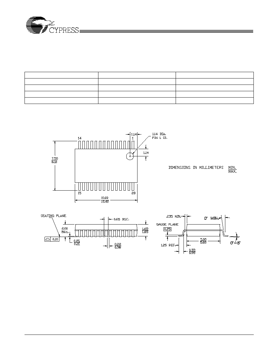
Package Drawing and Dimension
Pentium II is a registered trademarks of Intel Corporation. All product and company names mentioned in this document are
trademarks of their respective holders.
Ordering Information
Ordering Code
Package Type
Operating Range
CY2310BNZPVC≠1
28-pin SSOP
Commercial, 0 ∞C to 70∞C
CY2310BNZPVC≠1T
28-pin SSOP ≠ Tape and Reel
Commercial, 0 ∞C to 70∞C
CY2310BNZPVI≠1
28-pin SSOP
Industrial, ≠40 ∞C to 85∞C
CY2310BNZPVI≠1T
28-pin SSOP ≠ Tape and Reel
Industrial, ≠40 ∞C to 85∞C
28-lead (5.3 mm) Shrunk Small Outline Package O28
51-85079-*C
CY2310BNZ
Document #: 38-07260 Rev. *A
Page 6 of 6
Document History Page
Document Title: CY2310BNZ 3.3V 3.3V SDRAM Buffer for Mobile PCs with Four SO-DIMMs
Document Number: 38-07260
REV.
ECN NO.
Issue
Date
Orig. of
Change
Description of Change
**
110525
02/07/02
SZV
Change from Spec number: 38-01089 to 38-07260
*A
121577
01/29/03
RGL
Corrected the ordering information to match the devmaster.
Changed the max value of the VDD Core Supply in the Absolute Maximum
Conditions table from 4.6V to 7.0V