18 Output, 3.3V SDRAM Buffer for
Desktop PCs with 4 DIMMs
CY2318BNZ
Cypress Semiconductor Corporation
∑
3901 North First Street
∑
San Jose
∑
CA 95134
∑
408-943-2600
Document #: 38-07217 Rev. **
Revised December 4, 2001
Features
∑ One input to 18 output buffer/driver
∑ Supports up to four SDRAM DIMMs
∑ Two additional outputs for feedback
∑ SMBus interface for individual output control
∑ Low skew outputs (< 200 ps)
∑ Up to 100 MHz operation for Industrial temperatures
∑ Up to 133 MHz operation for Commercial temperatures
∑ Dedicated OE pin for testing
∑ Space-saving 48-pin SSOP package
∑ 3.3V operation
Functional Description
The CY2318BNZ is a 3.3V buffer designed to distribute
high-speed clocks in PC applications. The part has 18 outputs,
16 of which can be used to drive up to four SDRAM DIMMs,
and the remaining can be used for external feedback to a PLL.
The device operates at 3.3V and outputs can run up to 100
MHz, thus making it compatible with Pentium II
Æ
processors.
The CY2318BNZ can be used in conjunction with the CY2280,
CY2281, CY2282 or similar clock synthesizer for a complete
Pentium II motherboard solution.
The CY2318BNZ also includes an SMBus interface which can
enable or disable each output clock. On power-up, all output
clocks are enabled (internal pull up). A separate Output Enable
pin facilitates testing on ATE.
Pentium II is a registered trademark of Intel Corporation.
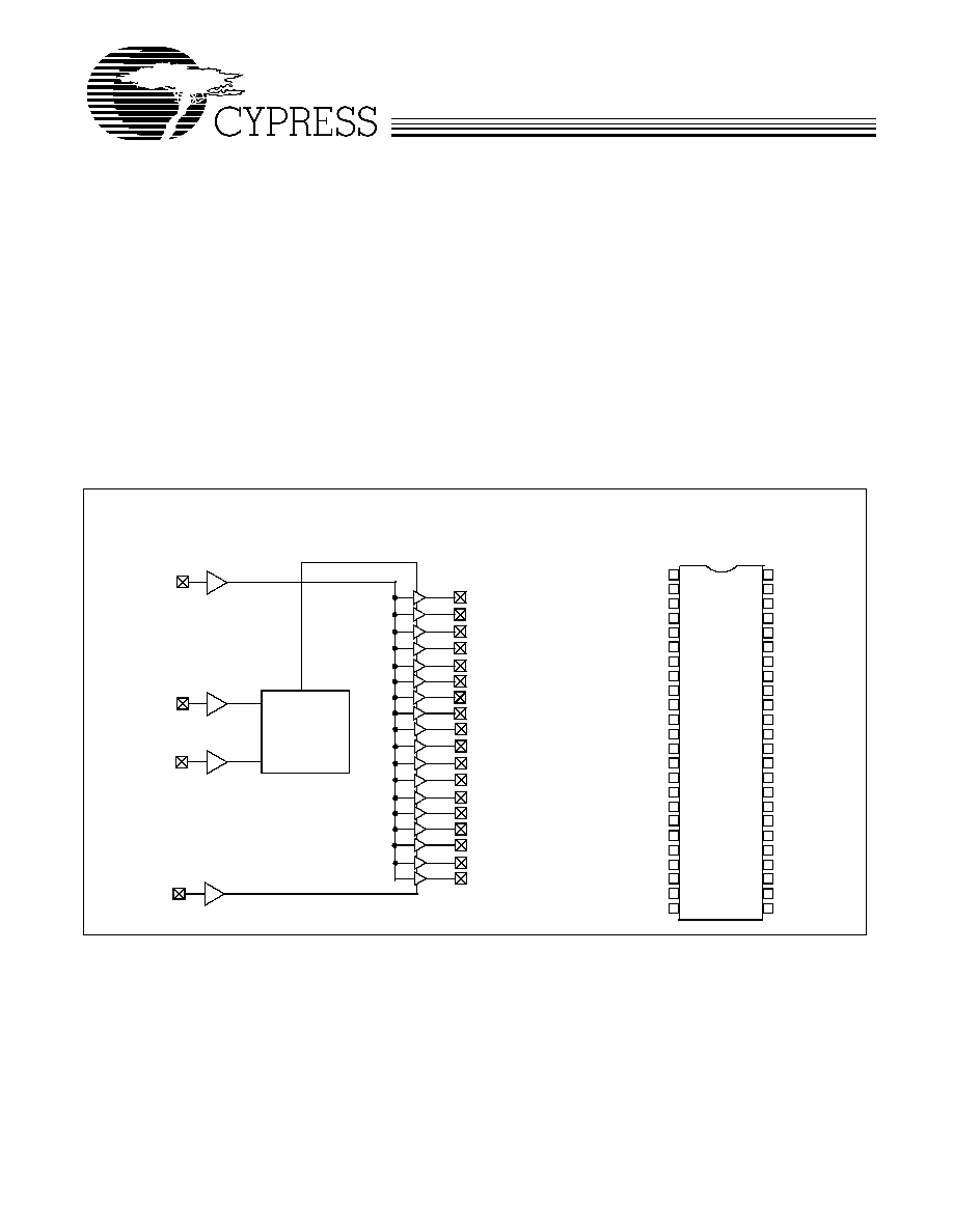
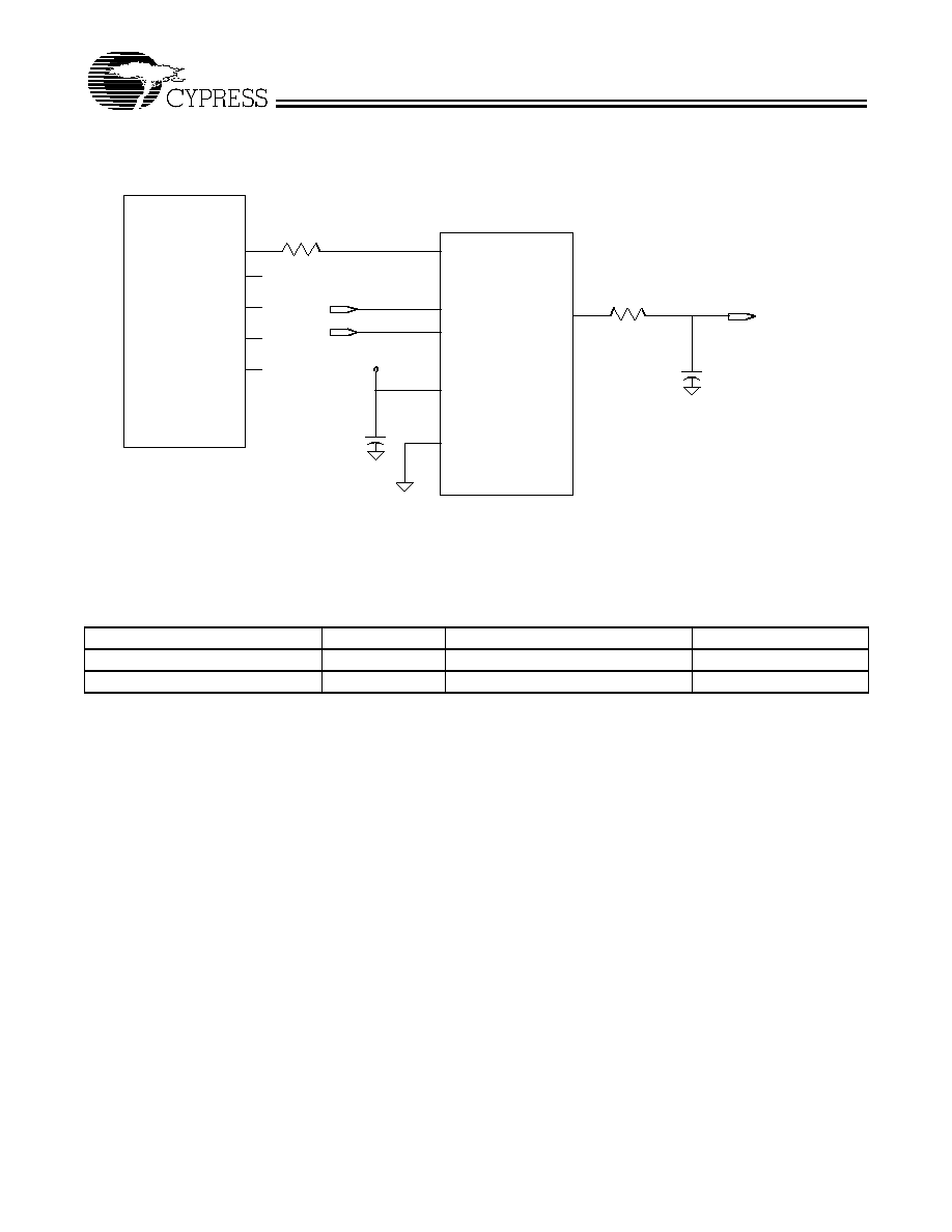
Block Diagram
SMBus
BUF_IN
SDATA
SCLOCK
SDRAM0
SDRAM1
SDRAM2
SDRAM3
SDRAM4
SDRAM5
SDRAM6
SDRAM7
1
2
3
4
NC
NC
V
DD
SDRAM15
SDRAM14
V
SS
V
DD
SDRAM13
SSOP
Top View
Pin Configuration
Decoding
8
5
6
7
12
9
10
11
13
14
15
16
20
17
18
19
24
21
22
23
48
47
46
45
41
44
43
42
37
40
39
38
36
35
34
33
29
32
31
30
25
28
27
26
SDRAM12
V
SS
OE
V
DD
SDRAM11
SDRAM10
V
SS
V
DD
SDRAM9
SDRAM8
V
SS
V
DD
SDRAM17
V
SS
V
SSIIC
SCLOCK
NC
NC
V
DD
SDRAM0
SDRAM1
V
SS
V
DD
SDRAM2
V
SS
BUF_IN
V
DD
SDRAM4
SDRAM5
V
SS
V
DD
SDRAM6
SDRAM7
V
SS
V
DD
SDRAM16
V
SS
V
DDIIC
SDATA
SDRAM3
SDRAM8
SDRAM9
SDRAM10
SDRAM11
SDRAM12
SDRAM13
SDRAM14
SDRAM15
SDRAM16
SDRAM17
OE
CY2318BNZ
Document #: 38-07217 Rev. **
Page 2 of 8
Device Functionality
Pin Summary
Name
Pins
Description
V
DD
3, 7, 12, 16, 20, 29, 33, 37, 42, 46
3.3V Digital voltage supply
V
SS
6, 10, 15, 19, 22, 27, 30, 34, 39, 43
Ground
V
DDIIC
23
SMBus Voltage supply
V
SSIIC
26
Ground for SMBus
BUF_IN
11
Input clock (5V tolerant)
OE
38
Output Enable (active HIGH), Three-state outputs when LOW
[1]
SDATA
24
SMBus data input
[1]
SCLK
25
SMBus clock input
[1]
SDRAM [0≠3]
4, 5, 8, 9
SDRAM byte 0 clock outputs
SDRAM [4≠7]
13, 14, 17, 18
SDRAM byte 1 clock outputs
SDRAM [8≠11]
31, 32, 35, 36
SDRAM byte 2 clock outputs
SDRAM [12≠15]
40, 41, 44, 45
SDRAM byte 3 clock outputs
SDRAM [16≠17]
21, 28
SDRAM clock outputs usable for feedback
N/C
1, 2, 47, 48
Reserved for future modifications, do not connect in system
Note:
1.
Internal pull-up resistor to V
DD
(value > 100 kohms).
OE
SDRAM [0≠17]
0
Hi-Z
1
1 x BUF_IN

CY2318BNZ
Document #: 38-07217 Rev. **
Page 3 of 8
Serial Configuration Map
∑ The Serial bits will be read by the clock driver in the following
order:
Byte 0 - Bits 7, 6, 5, 4, 3, 2, 1, 0
Byte 1 - Bits 7, 6, 5, 4, 3, 2, 1, 0
.
.
Byte N - Bits 7, 6, 5, 4, 3, 2, 1, 0
∑ Reserved and unused bits should be programmed to "0".
∑ SMBus Address for the CY2318BNZ is:
∑
∑
∑
∑
Maximum Ratings
Supply Voltage to Ground Potential ..................≠0.5 to +7.0V
DC Input Voltage (except BUF_IN) .......... ≠0.5V to V
DD
+ 0.5
DC Input Voltage (BUF_IN).............................. ≠0.5V to 7.0V
Storage Temperature .................................≠65
∞
C to +150
∞
C
Static Discharge Voltage
(per MIL-STD-883, Method 3015)..............................>2000V
Ambient Temperature under BIAS ..............≠55
∞
C to +125
∞
C
Absolute Maximum Ratings
Stresses greater than those listed in this table may cause per-
manent damage to the device. These represent a stress rating
only. Operation of the device at these or any other conditions
above those specified in the operating sections of this specifi-
cation is not implied. Maximum conditions for extended peri-
ods may affect reliability.
A6
A5
A4
A3
A2
A1
A0
R/W
1
1
0
1
0
0
1
----
Byte 0:SDRAM Active/Inactive Register
(1 = Active, 0 = Inactive), Default = Active
Bit
Pin #
Description
Bit 7 18
SDRAM7 (Active/Inactive)
Bit 6 17
SDRAM6 (Active/Inactive)
Bit 5 14
SDRAM5 (Active/Inactive)
Bit 4 13
SDRAM4 (Active/Inactive)
Bit 3 9
SDRAM3 (Active/Inactive)
Bit 2 8
SDRAM2 (Active/Inactive)
Bit 1 5
SDRAM1 (Active/Inactive)
Bit 0 4
SDRAM0 (Active/Inactive)
Byte 1: SDRAM Active/Inactive Register
(1 = Active, 0 = Inactive), Default = Active
Bit
Pin #
Description
Bit 7
45
SDRAM15 (Active/Inactive)
Bit 6
44
SDRAM14 (Active/Inactive)
Bit 5
41
SDRAM13 (Active/Inactive)
Bit 4
40
SDRAM12 (Active/Inactive)
Bit 3
36
SDRAM11 (Active/Inactive)
Bit 2
35
SDRAM10 (Active/Inactive)
Bit 1
32
SDRAM9 (Active/Inactive)
Bit 0
31
SDRAM8 (Active/Inactive)
Byte 2: SDRAM Active/Inactive Register
(1 = Active, 0 = Inactive), Default = Active
Bit
Pin #
Description
Bit 7
28
SDRAM17 (Active/Inactive)
Bit 6
21
SDRAM16 (Active/Inactive)
Bit 5
--
Reserved, drive to 0
Bit 4
--
Reserved, drive to 0
Bit 3
--
Reserved, drive to 0
Bit 2
--
Reserved, drive to 0
Bit 1
--
Reserved, drive to 0
Bit 0
--
Reserved, drive to 0
Parameter
Description
Rating
Unit
V
DD
, V
IN
Voltage on Any Pin with Respect to GND
≠0.5 to +7.0
V
T
STG
Storage Temperature
≠65 to +150
∞C
T
A
Operating Temperature
0 to +70
∞C
T
B
Ambient Temperature under Bias
≠55 to +125
∞C
Operating Conditions
Parameter
Description
Min.
Max.
Unit
V
DD
, V
DDIIC
Supply Voltage
3.135
3.465
V
T
A
Operating Temperature (Ambient Temperature)
≠40
85
∞C
C
L
Load Capacitance
20
30
pF
C
IN
Input Capacitance
7
pF
CY2318BNZ
Document #: 38-07217 Rev. **
Page 4 of 8
DC Electrical Characteristics:
T
A
= -40∞C to +85∞C, V
DDQ3
= 3.3V±5%
Parameter
Description
Test Condition/
Comments
Min
Typ
Max
Unit
I
DD
3.3V Supply Current
BUF_IN = 64 MHz
140
165
200
mA
I
DD Tristate
3.3V Supply Current in Three-state
BUF_IN = 100 MHz
5
mA
Logic Inputs (BUF_IN, OE, SCLOCK, SDATA)
V
IL
Input Low Voltage
GND≠0.3
0.8
V
V
IH
Input High Voltage
2.0
V
DDQ3
+ 0.5
V
I
ILEAK
Input Leakage Current, BUF_IN
≠5
+5
µA
I
ILEAK
Input Leakage Current
[2]
≠20
+5
µA
Logic Outputs (SDRAM0:17)
[3]
V
OL
Output Low Voltage
I
OL
= 1 mA
50
mV
V
OH
Output High Voltage
I
OH
= ≠1 mA
3.1
V
I
OL
Output Low Current
V
OL
= 1.5V
70
110
185
mA
I
OH
Output High Current
V
OH
= 1.5V
65
100
160
mA
Pin Capacitance/Inductance
C
IN
Input Pin Capacitance (Except
BUF_IN)
5
pF
C
OUT
Output Pin Capacitance
6
pF
L
IN
Input Pin Inductance
7
nH
CY2318BNZ
Document #: 38-07217 Rev. **
Page 5 of 8
AC Electrical Characteristics:
T
A
= ≠40∞C to +85∞C, V
DDQ3
= 3.3V±5% (Lump Capacitance Test Load = 30 pF)
Parameter
Description
Test Condition
Min
Typ
Max
Unit
f
IN
Input Frequency
Commercial Temperature
Range
0
133
MHz
t
R
Output Rise Edge Rate
Measured from 0.4V to 2.4V
1.5
4.0
V/ns
t
F
Output Fall Edge Rate
Measured from 2.4V to 0.4V
1.5
4.0
V/ns
t
SR
Output Skew, Rising Edges
200
ps
t
SF
Output Skew, Falling Edges
200
ps
t
EN
Output Enable Time
1.0
8.0
ns
t
DIS
Output Disable Time
1.0
8.0
ns
t
PR
Rising Edge Propagation Delay
3.0
3.85
5.0
ns
t
PF
Falling Edge Propagation Delay
3.0
3.85
5.0
ns
t
D
Duty Cycle
Measured at 1.5V
50
60
%
Z
o
AC Output Impedance
15
Notes:
2.
OE, SCLOCK, and SDATA logic pins have a 250-k
internal pull-up resistor (not CMOS level).
3.
Outputs loaded by 6" 60
transmission lines with 20-pF capacitors.
0.1
µ
F
V
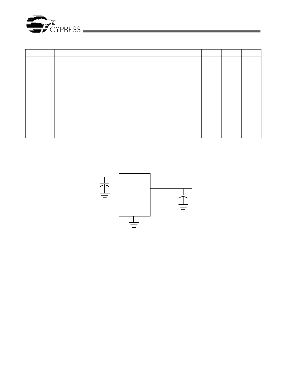
DD
CLK out
C
LOAD
OUTPUTS
GND
Test Circuit
CY2318BNZ
Document #: 38-07217 Rev. **
Page 6 of 8
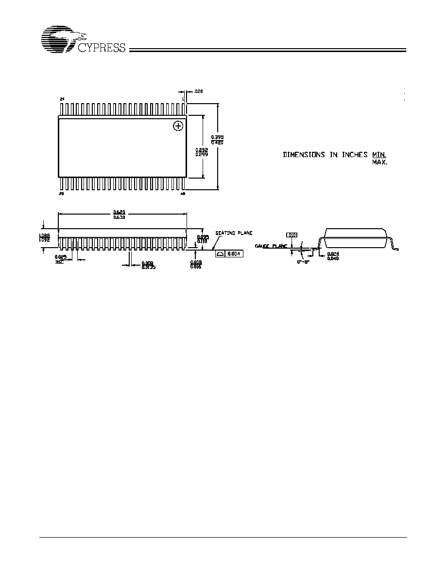
Package Diagram
Application Circuit
C
d
= DECOUP LING CAPACITOR S
C
t
= OPTIONAL EMI-R EDUCING CAP ACI TORS
R
s
= SERIES TERMINATING RESISTORS
* CY2280 48 PIN SSOP
(or CY2281 or CY2282)
CY2313 28 PIN SOIC
C
d
0.1uF
V
DD
3.3V
V
SS
BUF_IN
V
DD
C
t
SDRAM ( 0-12)
SDRAM ( 0-12)
SDATA
SCLK
R
s
SDATA
SCLK
CPUCLK
PCICLK
USBCLK
REF
APIC
R
s
* THIS FREQUENCY SYNTHESIZER IS USED TO
GENERATE CPU, PCI, USB, REF, AND APIC CLOCKS.
CY2313A: 28-PIN SOIC
Ordering Information
Ordering Code
Package Name
Package Type
Operating Range
CY2318BNZPVI-11
O48
48-Pin SSOP
Industrial (≠40∞C to 85∞C)
CY2318BNZPVC-11
O48
48-Pin SSOP
Commercial (0∞C to 70∞C)
CY2318BNZ
Document #: 38-07217 Rev. **
Page 7 of 8
© Cypress Semiconductor Corporation, 2001. The information contained herein is subject to change without notice. Cypress Semiconductor Corporation assumes no responsibility for the use
of any circuitry other than circuitry embodied in a Cypress Semiconductor product. Nor does it convey or imply any license under patent or other rights. Cypress Semiconductor does not authorize
its products for use as critical components in life-support systems where a malfunction or failure may reasonably be expected to result in significant injury to the user. The inclusion of Cypress
Semiconductor products in life-support systems application implies that the manufacturer assumes all risk of such use and in doing so indemnifies Cypress Semiconductor against all charges.
48-Lead Shrunk Small Outline Package O48
51-85061-B

CY2318BNZ
Document #: 38-07217 Rev. **
Page 8 of 8
Revision History
Document Title: CY2318BNZ 18 Output, 3.3V SDRAM Buffer for Desktop PCs with 4 DIMMs
Document Number: 38-07217
REV.
ECN NO.
Issue
Date
Orig. of
Change
Description of Change
**
111855
12/09/01
DSG
Change from Spec number: 38-01091 to 38-07217