200-MHz Field Programmable Zero Delay Buffer
CY23FP12
Cypress Semiconductor Corporation
∑
3901 North First Street
∑
San Jose
,
CA 95134
∑
408-943-2600
Document #: 38-07246 Rev. *E
Revised December 13, 2004
Features
∑ Fully field-programmable
-- Input and output dividers
-- Inverting/noninverting outputs
-- Phase-locked loop (PLL) or fanout buffer configu-
ration
∑ 10-MHz to 200-MHz operating range
∑ Split 2.5V or 3.3V outputs
∑ Two LVCMOS reference inputs
∑ Twelve low-skew outputs
-- 35ps typ. output-to-output skew (same freq)
∑ 110 ps typ. cycle-cycle jitter (same freq)
∑ Three-stateable outputs
∑ < 50-
µA shutdown current
∑ Spread Aware
∑ 28-pin SSOP
∑ 3.3V operation
∑ Industrial temperature available
Functional Description
The CY23FP12 is a high-performance fully field-program-
mable 200 MHz zero delay buffer designed for high speed
clock distribution. The integrated PLL is designed for low jitter
and optimized for noise rejection. These parameters are
critical for reference clock distribution in systems using
high-performance ASICs and microprocessors.
The CY23FP12 is fully programmable via volume or prototype
programmers enabling the user to define an appli-
cation-specific Zero Delay Buffer with customized input and
output dividers, feedback topology (internal/external), output
inversions, and output drive strengths. For additional flexibility,
the user can mix and match multiple functions, listed in
Table 2, and assign a particular function set to any one of the
four possible S1-S2 control bit combinations. This feature
allows for the implementation of four distinct personalities,
selectable with S1-S2 bits, on a single programmed silicon.
The CY23FP12 also features a proprietary auto-power-down
circuit that shuts down the device in case of a REF failure,
resulting in less than 50
µA of current draw.
The CY23FP12 provides twelve outputs grouped in two banks
with separate power supply pins which can be connected
independently to either a 2.5V or a 3.3V rail.
Selectable reference input is a fault tolerance feature which
allows for glitch-free switch over to secondary clock source
when REFSEL is asserted/deasserted.
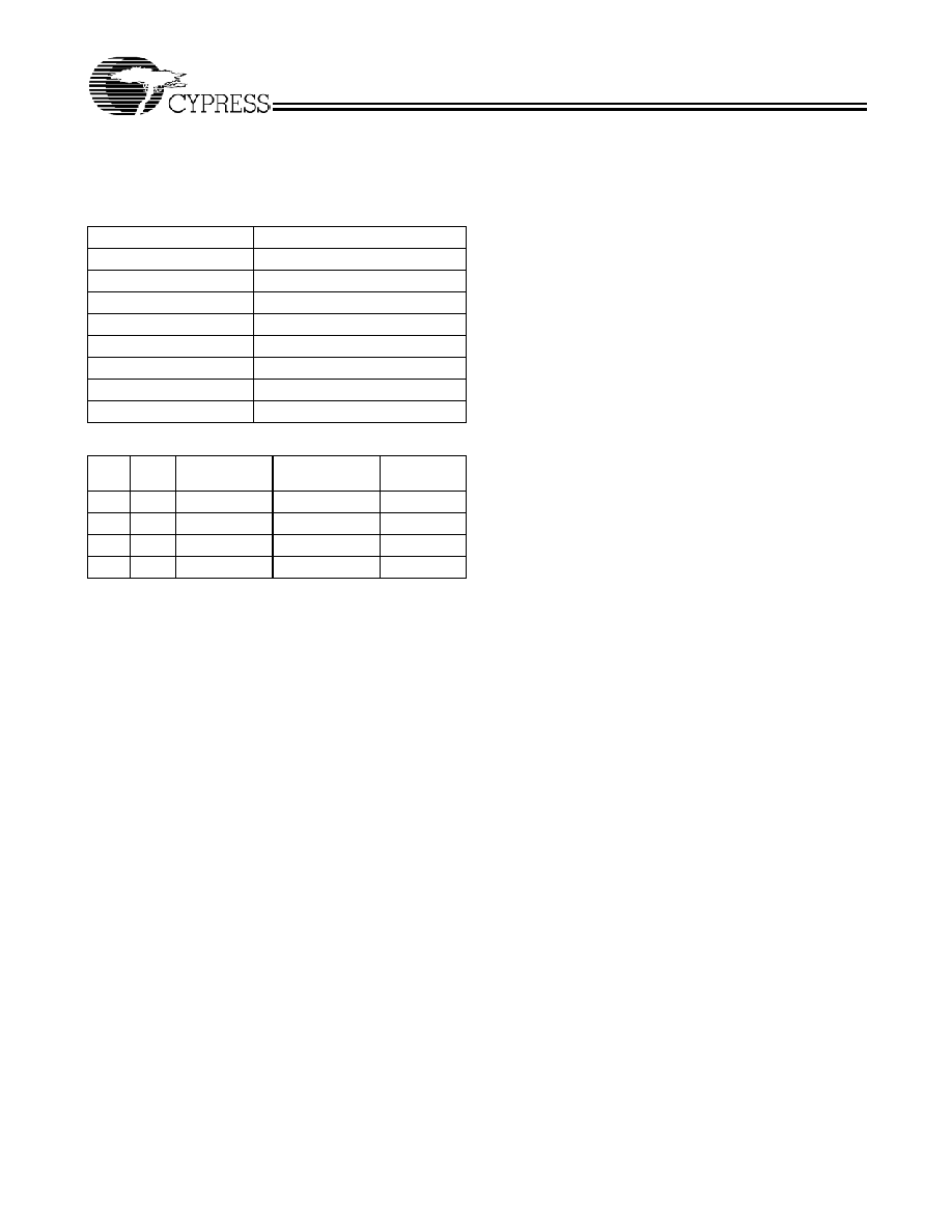
21
28
REFSEL
FBK
CLKA0
CLKA1
V
SSA
CLKA2
CLKA3
V
DDA
1
2
3
4
5
6
7
8
22
23
24
25
26
27
REF2
REF1
CLKB0
CLKB1
V
SSB
CLKB2
CLKB3
V
DDB
SSOP
Top View
Pin Configuration
17
V
DDA
20
V
SSA
19
CLKA4
18
CLKA5
16
V
SSC
15
S1
9
V
SSB
12
V
DDB
13
V
DDC
10
CLKB4
11
CLKB5
14
S2
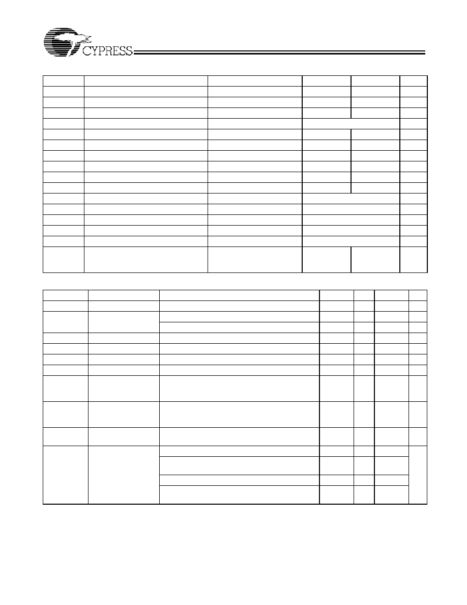
FBK
˜
M
˜
N
100 to
400MHz
PLL
CLKA1
CLKA3
CLKA2
REF2
REFSEL
CLKA4
CLKA5
CLKB1
CLKB3
CLKB2
CLKB4
CLKB5
VDDA
VSSA
VDDB
VSSB
˜
2
˜
3
˜
4
˜
X
CLKA0
VDDC
VSSC
˜
1
Lock Detect
Test Logic
REF1
CLKB0
S[2:1]
Function
Selection
Block Diagram
CY23FP12
Document #: 38-07246 Rev. *E
Page 2 of 10
.
Pin Description
Pin
Name
I/O
Type
Description
1
REF2
I
LVTTL/LVCMOS
Input reference frequency, 5V-tolerant input.
2
REF1
I
LVTTL/LVCMOS
Input reference frequency, 5V-tolerant input.
3
CLKB0
O
LVTTL
Clock output, Bank B.
4
CLKB1
O
LVTTL
Clock output, Bank B.
5
V
SSB
PWR
POWER
Ground for Bank B.
6
CLKB2
O
LVTTL
Clock output, Bank B.
7
CLKB3
O
LVTTL
Clock output, Bank B.
8
V
DDB
PWR
POWER
2.5V or 3.3V supply, Bank B.
9
V
SSB
PWR
POWER
Ground for Bank B.
10
CLKB4
O
LVTTL
Clock output, Bank B.
11
CLKB5
O
LVTTL
Clock output, Bank B.
12
V
DDB
PWR
POWER
2.5V or 3.3V supply, Bank B.
13
V
DDC
PWR
POWER
3.3V core supply.
14
S2
I
LVTTL
Select input.
15
S1
I
LVTTL
Select input.
16
V
SSC
PWR
POWER
Ground for core.
17
V
DDA
PWR
POWER
2.5V or 3.3V supply, Bank A.
18
CLKA5
O
LVTTL
Clock output, Bank A.
19
CLKA4
O
LVTTL
Clock output, Bank A.
20
V
SSA
PWR
POWER
Ground for Bank A.
21
V
DDA
PWR
POWER
2.5V or 3.3V supply Bank A.
22
CLKA3
O
LVTTL
Clock output, Bank A.
23
CLKA2
O
LVTTL
Clock output, Bank A.
24
V
SSA
PWR
POWER
Ground for Bank A.
25
CLKA1
O
LVTTL
Clock output, Bank A.
26
CLKA0
O
LVTTL
CLock output, Bank A.
27
FBK
I
LVTTL
PLL feedback input.
28
REFSEL
I
LVTTL
Reference select input. REFSEL = 0, REF1 is
selected. REFSEL = 1, REF2 is selected.
CY23FP12
Document #: 38-07246 Rev. *E
Page 3 of 10
Below is a list of independent functions that can be
programmed with a volume or prototype programmer on the
"default" silicon.
/1,/2,/3,/4,
/x,/2x
/1,/2,/3,/4,
/x,/2x
/1,/2,/3,/4,
/x,/2x
/1,/2,/3,/4,
/x,/2x
/1,/2,/3,/4,
/x,/2x
/1,/2,/3,/4,
/x,/2x
PLL
/M
/N
Output
Function
Select
Matrix
REF
FBK
CLKB5
CLKB4
CLKB3
CLKB2
CLKB1
CLKB0
CLKA5
CLKA4
CLKA3
CLKA2
CLKA1
CLKA0
Figure 1. Basic PLL Block Diagram
Table 1.
Configuration
Description
Default
DC Drive Bank A
Programs the drive strength of Bank A outputs. The user can select one out
of two possible drive strength settings that produce output DC currents in the
range of ±16 mA to ±20 mA.
+16 mA
DC Drive Bank B
Programs the drive strength of Bank B outputs. The user can select one out
of two possible drive strength settings that produce output DC currents in the
range of ±16 mA to ±20 mA.
+16 mA
Output Enable for Bank B clocks
Enables/Disables CLKB[5:0] outputs. Each of the six outputs can be disabled
individually if not used, to minimize electromagnetic interference (EMI) and
switching noise.
Enable
Output Enable for Bank A clocks
Enables/Disables CLKA[5:0] outputs. Each of the six outputs can be disabled
individually if not used, to minimize EMI and switching noise.
Enable
Inv CLKA0
Generates an inverted clock on the CLKA0 output. When this option is
programmed, CLKA0 and CLKA1 will become complimentary pairs.
Non-invert
Inv CLKA2
Generates an inverted clock on the CLKA2 output. When this option is
programmed, CLKA2 and CLKA3 will become complimentary pairs.
Non-invert
Inv CLKA4
Generates an inverted clock on the CLKA4 output. When this option is
programmed, CLKA4 and CLKA5 will become complimentary pairs.
Non-invert
Inv CLKB0
Generates an inverted clock on the CLKB0 output. When this option is
programmed, CLKB0 and CLKB1 will become complimentary pairs.
Non-invert
Inv CLKB2
Generates an inverted clock on the CLKB2 output. When this option is
programmed, CLKB2 and CLKB3 will become complimentary pairs.
Non-invert
CY23FP12
Document #: 38-07246 Rev. *E
Page 4 of 10
Below is a list of independent functions, which can be
assigned to each of the four S1 and S2 combinations. When
a particular S1 and S2 combination is selected, the device will
assume the configuration (which is essentially a set of
functions given in Table 2, below) that has been preassigned
to that particular combination.
Inv CLKB4
Generates an inverted clock on the CLKB4 output. When this option is
programmed, CLKB4 and CLKB5 will become complimentary pairs.
Non-invert
Pull-down Enable
Enables/Disables internal pulldowns on all outputs
Enable
Fbk Pull-down Enable
Enables/Disables internal pulldowns on the feedback path (applicable to both
internal and external feedback topologies)
Enable
Fbk Sel
Selects between the internal and the external feedback topologies
External
Table 1. (continued)
Configuration
Description
Default
Table 2.
Function
Description
Default
Output Enable CLKB[5:4] Enables/Disables CLKB[5:4] output pair
Enable
Output Enable CLKB[3:2] Enables/Disables CLKB[3:2] output pair
Enable
Output Enable CLKB[1:0] Enables/Disables CLKB[1:0] output pair
Enable
Output Enable CLKA[5:4] Enables/Disables CLKA[5:4] output pair
Enable
Output Enable CLKA[3:2] Enables/Disables CLKA[3:2] output pair
Enable
Output Enable CLKA[1:0] Enables/Disables CLKA[1:0] output pair
Enable
Auto Power-down Enable Enables/Disables the auto power down circuit, which monitors the reference clock rising
edges and shuts down the device in case of a reference "failure." This failure is triggered
by a drift in reference frequency below a set limit. This auto power down circuit is
disabled internally when one or more of the outputs are configured to be driven directly
from the reference clock.
Enable
PLL Power-down
Shuts down the PLL when the device is configured as a non-PLL fanout buffer.
PLL Enabled
M[7:0]
Assigns an eight-bit value to reference divider ≠M. The divider can be any integer value
from 1 to 256; however, the PLL input frequency cannot be lower than 10 MHz.
2
N[7:0]
Assigns an eight-bit value to feedback divider ≠N. The divider can be any integer value
from 1 to 256; however, the PLL input frequency cannot be lower than 10 MHz.
2
X[6:0]
Assigns a seven-bit value to output divider ≠X. The divider can be any integer value
from 5 to 130. Divide by 1,2,3, and 4 are preprogrammed on the device and can be
activated by the appropriate output mux setting.
1
Divider Source
Selects between the PLL output and the reference clock as the source clock for the
output dividers.
PLL
CLKA54 Source
Independently selects one out of the eight possible output dividers that will connect to
the CLKA5 and CLKA4 pair. Please refer to Table 3 for a list of divider values.
Divide by 2
CLKA32 Source
Independently selects one out of the eight possible output dividers that will connect to
the CLKA3 and CLKA2 pair. Please refer to Table 3 for a list of divider values.
Divide by 2
CLKA10 Source
Independently selects one out of the eight possible output dividers that will connect to
the CLKA1 and CLKA0 pair. Please refer to Table 3 for a list of divider values.
Divide by 2
CLKB54 Source
Independently selects one out of the eight possible output dividers that will connect to
the CLKB5 and CLKB4 pair. Please refer to Table 3 for a list of divider values.
Divide by 2
CLKB32 Source
Independently selects one out of the eight possible output dividers that will connect to
the CLKB3 and CLKB2 pair. Please refer to Table 3 for a list of divider values.
Divide by 2
CLKB10 Source
Independently selects one out of the eight possible output dividers that will connect to
the CLKB1 and CLKB0 pair. Please refer to Table 3 for a list of divider values.
Divide by 2
CY23FP12
Document #: 38-07246 Rev. *E
Page 5 of 10
Table 3 is a list of output dividers that are independently
selected to connect to each output pair.
In the default (non-programmable) state of the device, S1 and
S2 pins will function, as indicated in Table 4.
Field Programming the CY23FP12
The CY23FP12 is programmed at the package level, i.e. in a
programmer socket. The CY23FP12 is flash-technology
based, so the parts can be reprogrammed up to 100 times.
This allows for fast and easy design changes and product
updates, and eliminates any issues with old and out-of-date
inventory.
Samples and small prototype quantities can be programmed
on the CY3672 programmer. Cypress's value-added distri-
bution partners and third-party programming systems from BP
Microsystems, HiLo Systems, and others are available for
large production quantities.
CyberClocks
Software
CyberClocks is an easy-to-use software application that
allows the user to custom-configure the CY23FP12. Users can
specify the REF, PLL frequency, output frequencies and/or
post-dividers, and different functional options. CyberClocks
outputs an industry standard JEDEC file used for
programming the CY23FP12.
CyberClocks can be downloaded free of charge from the
Cypress website at www.cypress.com.
CY3672 FTG Development Kit
The Cypress CY3672 FTG Development Kit comes complete
with everything needed to design with the CY23FP12 and
program samples and small prototype quantities. The kit
comes with the latest version of CyberClocks and a small
portable programmer that connects to a PC serial port for
on-the-fly programming of custom frequencies.
The JEDEC file output of CyberClocks can be downloaded to
the portable programmer for small-volume programming, or
for use with a production programming system for larger
volumes.
CY23FP12 Frequency Calculation
The CY23FP12 is an extremely flexible clock buffer with up to
twelve individual outputs, generated from an integrated PLL.
There are four variables used to determine the final output
frequency. These are the input Reference Frequency M, the N
dividers, and the post divider X.
The basic PLL block diagram is shown in Figure 1. Each of the
six clock outputs pair has many output options available to it.
There are six post divider options: /1, /2, /3, /4, /X, and /2X.
The post divider options can be applied to the calculated PLL
frequency or to the REF directly. The feedback either is
connected to CLKA0 internally or connected to any output
externally.
A programmable divider, M, is inserted between the reference
input, REF, and the phase detector. The divider M can be any
integer 1 to 256. The PLL input frequency cannot be lower than
10 MHz or higher than 200 MHz.
A programmable divider, N, is inserted between the feedback
input, FBK, and the phase detector. The divider N can be any
integer 1 to 256. The PLL input frequency cannot be lower than
10 MHz or higher than 200 MHz.
So the output can be calculated as following:
F
REF
/ M = F
FBK
/ N.
F
PLL
= (F
REF
* N *
post divider)/M.
F
OUT
= F
PLL
/ post divider.
In addition to above divider options, the another option
bypasses the PLL and passes the REF directly to the output.
F
OUT
= F
REF
.
Note:
1. Outputs will be rising edge aligned only to those outputs using this same device setting.
2. When the source of an output pair is set to [111], the output pair becomes lock indicator signal. For example, if the source of an output pair (CLKA0, CLKA1) is
set to [111], the CLKA0 and CLKA1, becomes lock indicator signals. In non-invert mode, CLKA0 and CLKA1 signals will be high when the PLL is in lock mode. If
CLKA0 is in an invert mode, the CLKA0 will be low and the CLKA1 will be high when the PLL is in lock mode.
Table 3.
CLKA/B Source
Output Connects To
0 [000]
REF
1 [001]
Divide by 1
2 [010]
Divide by 2
3 [011]
Divide by 3
4 [100]
Divide by 4
5 [101]
Divide by X
6 [110]
Divide by 2X
[1]
7 [111]
TEST mode [LOCK signal]
[2]
Table 4.
S2
S1
CLKA[5:0]
CLKB[5:0]
Output
Source
0
0
Three-state
Three-state
PLL
0
1
Driven
Three-state
PLL
1
0
Driven
Driven
Reference
1
1
Driven
Driven
PLL
CY23FP12
Document #: 38-07246 Rev. *E
Page 6 of 10
Absolute Maximum Conditions
Parameter
Description
Condition
Min.
Max.
Unit
V
DD
Supply Voltage
Non-functional
≠0.5
7
VDC
V
IN
Input Voltage REF
Relative to V
CC
≠0.5
7
VDC
V
IN
Input Voltage Except REF
Relative to V
CC
≠0.5
V
DD
+ 0.5
VDC
LU
I
Latch-up Immunity
Functional
300
mA
T
S
Temperature, Storage
Non-functional
≠65
+125
∞C
T
A
Temperature, Operating Ambient
Commercial Temperature
0
+70
∞C
T
A
Temperature, Operating Ambient
Industrial Temperature
≠40
+85
∞C
T
J
Junction Temperature
Industrial Temperature
125
∞C
ÿ
Jc
Dissipation, Junction to Case
Functional
34
∞C/W
ÿ
Ja
Dissipation, Junction to Ambient
Functional
86
∞C/W
ESD
h
ESD Protection (Human Body Model)
2000
V
M
SL
Moisture Sensitivity Level
MSL ≠ 1
class
G
ATES
Total Functional Gate Count
Assembled Die
21375
each
UL≠94
Flammability Rating
@ 1/8 in.
V≠0
class
FIT
Failure in Time
Manufacturing test
10
ppm
T
PU
Power-up time for all V
DD
s to reach
minimum specified voltage (power
ramps must be monotonic)
0.05
500
ms
DC Electrical Specifications for CY23FP12SC/I Commercial/Industrial Temperature Devices
Parameter
Description
Test Conditions
Min.
Typ.
Max.
Unit
V
DDC
Core Supply Voltage
3.135
3.465
V
V
DDA
, V
DDB
Bank A, Bank B
Supply Voltage
3.135
3.465
V
2.375
2.625
V
V
IL
Input LOW Voltage
[3]
0.3 ◊ V
DD
V
V
IH
Input HIGH Voltage
[3]
0.7 ◊ V
DD
V
I
IL
Input LOW Current
[3]
V
IN
= 0V
50.0
µA
I
IH
Input HIGH Current
[3]
V
IN
= V
DD
50.0
µA
V
OL
Output LOW Voltage
[4]
V
DDA
/V
DDB
= 3.3V, I
OL
= 16 mA (standard drive)
V
DDA
/V
DDB
= 3.3V, I
OL
= 20 mA (high drive)
V
DDA
/V
DDB
= 2.5V, I
OL
= 16 mA (high drive)
0.5
V
V
OH
Output HIGH
Voltage
[4]
V
DDA
/V
DDB
= 3.3V, I
OH
= ≠16 mA (standard drive)
V
DDA
/V
DDB
= 3.3V, I
OH
= ≠20 mA (high drive)
V
DDA
/V
DDB
= 2.5V, I
OH
= ≠16 mA (high drive)
V
DD
≠ 0.5
V
I
DDS
Power-down Supply
Current
REF = 0 MHz
12
50
µA
I
DD
Supply Current
V
DDA
= V
DDB
= 2.5V, Unloaded outputs @ 166 MHz
40
65.0
mA
V
DDA
= V
DDB
= 2.5V, Loaded outputs @ 166 MHz,
C
L
= 15 pF
65
100
V
DDA
= V
DDB
= 3.3V, Unloaded outputs @ 166 MHz
50
80
V
DDA
= V
DDB
= 3.3V, Loaded outputs @ 166 MHz,
C
L
= 15 pF
100
120
Notes:
3. Applies to both Ref Clock and FBK.
4. Parameter is guaranteed by design and characterization. Not 100% tested in production.
CY23FP12
Document #: 38-07246 Rev. *E
Page 7 of 10
Switching Characteristics
[5]
Parameter
Description
Test Conditions
Min.
Typ.
Max.
Unit
Reference Frequency
[6]
10
200
MHz
Reference Edge Rate
1
V/ns
Reference Duty Cycle
25
75
%
t
1
Output Frequency
[7]
C
L
= 15 pF, Commercial Temperature
10
200
MHz
C
L
= 15 pF, Industrial Temperature
10
166.7
C
L
= 30 pF, Commercial Temperature
10
100
C
L
= 30 pF, Industrial Temperature
10
83.3
Duty Cycle
[5]
V
DDA/B
= 3.3V, measured at V
DD
/2
45.0
50.0
55.0
%
V
DDA/B
= 2.5V
40.0
50.0
60.0
t
3
Rise Time
[5]
V
DDA/B
= 3.3V, 0.8V to 2.0V,
C
L
= 30 pF (standard drive and high drive)
1.6
ns
V
DDA/B
= 3.3V, 0.8V to 2.0V,
C
L
= 15 pF (standard drive and high drive)
0.8
V
DDA/B
= 2.5V, 0.6V to 1.8V,
C
L
= 30 pF (high drive only)
2.0
V
DDA/B
= 2.5V, 0.6V to 1.8V,
C
L
= 15 pF (high drive only)
1.0
t
4
Fall Time
[5]
V
DDA/B
= 3.3V, 0.8V to 2.0V,
C
L
= 30 pF (standard drive and high drive)
1.6
ns
V
DDA/B
= 3.3V, 0.8V to 2.0V,
C
L
= 15 pF (standard drive and high drive)
0.8
V
DDA/B
= 2.5V, 0.6V to 1.8V,
C
L
= 30 pF (high drive only)
1.6
V
DDA/B
= 2.5V, 0.6V to 1.8V,
C
L
= 15 pF (high drive only)
0.8
TTB
Total Timing Budget,
[8,9]
Bank A and B same
frequency
Outputs @200 MHz, tracking skew not
included
650
ps
Total Timing Budget, Bank
A and B different frequency
850
t
5
Output to Output Skew
[5]
All outputs equally loaded
35
[10]
200
ps
Bank to Bank Skew
Same frequency
200
Bank to Bank Skew
Different frequency
400
Bank to Bank Skew
Different voltage, same frequency
400
t
6
Input to Output Skew (static
phase offset)
[5]
Measured at V
DD
/2, REF to FBK
0
250
ps
t
7
Device to Device Skew
[5]
Measured at V
DD
/2
0
500
ps
t
J
Cycle to Cycle Jitter
[5]
(Peak)
Bank A and B same frequency
110
[11]
200
ps
Cycle to Cycle Jitter
[5]
(Peak)
Bank A and B different frequency
400
Notes:
5. All parameters are specified with loaded outputs.
6. When the device is configured as a non-PLL fanout buffer (PLL Power-down enabled), the reference frequency can be lower than 10MHz. With auto power-down
disabled and PLL power-down enabled, the reference frequency can be as low as DC level.
7. When the device is configured as a non-PLL fanout buffer (PLL Power-down enabled), the output frequency can be lower than 10MHz. With auto power-down
disabled and PLL power-down enabled, the output frequency can be as low as DC level.
8. Guaranteed by statistical correlation. Tested initially and after any design or process changes that may affect these parameters.
9. TTB is the window between the earliest and the latest output clocks with respect to the input reference clock across variations in output frequency, supply voltage,
operating temperature, input clock edge rate, and process. The measurements are taken with the AC test load specified and include output-output skew,
cycle-cycle jitter, and dynamic phase error.TTB will be equal to or smaller than the maximum specified value at a given frequency.
10. Same frequency, 15pF load, high drive.
11. Same frequency, 15pF load, low drive.
CY23FP12
Document #: 38-07246 Rev. *E
Page 8 of 10
t
tsk
Tracking Skew
Input reference clock @ < 50-KHz modulation
with ±3.75% spread
200
ps
t
LOCK
PLL Lock Time
[5]
Stable power supply, valid clock at REF
1.0
ms
T
LD
Inserted Loop Delay
Max loop delay for PLL Lock (stable
frequency)
7
ns
Max loop delay to meet Tracking Skew Spec
4
ns
Switching Characteristics
[5]
Parameter
Description
Test Conditions
Min.
Typ.
Max.
Unit
Switching Waveforms
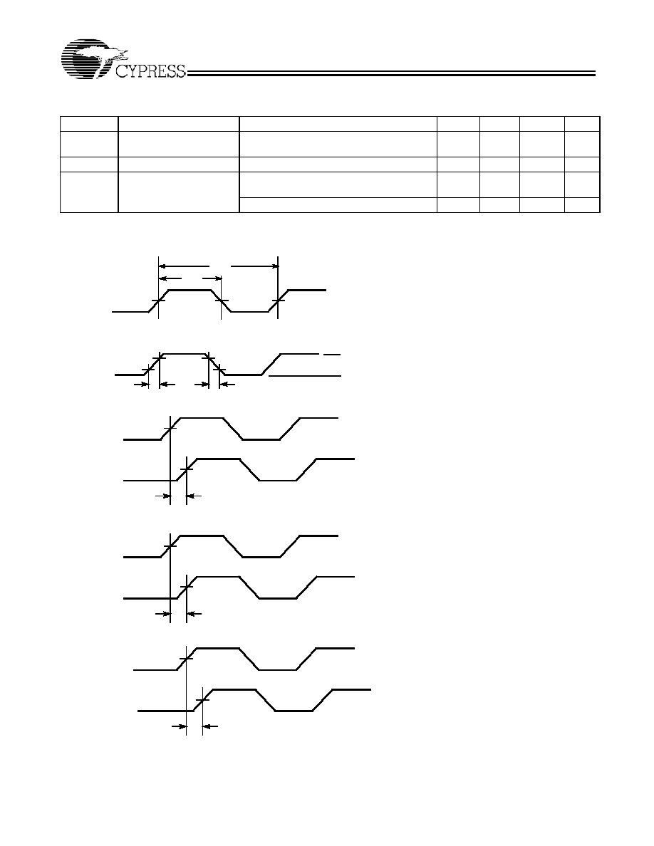
Duty Cycle Timing
t
1
t
2
1.4V
1.4V
1.4V
OUTPUT
t
3
3.3V
0V
0.8V
2.0V
2.0V
0.8V
t
4
All Outputs Rise/Fall Time
Output-Output Skew
1.4V
t
5
OUTPUT
OUTPUT
1.4V
Input-Output Propagation Delay
V
DD
/2
t
6
INPUT
FBK
V
DD
/2
V
DD
/2
V
DD
/2
t
7
FBK, Device 1
FBK, Device 2
Device-Device Skew
CY23FP12
Document #: 38-07246 Rev. *E
Page 9 of 10
© Cypress Semiconductor Corporation, 2004. The information contained herein is subject to change without notice. Cypress Semiconductor Corporation assumes no responsibility for the use
of any circuitry other than circuitry embodied in a Cypress product. Nor does it convey or imply any license under patent or other rights. Cypress products are not warranted nor intended to be
used for medical, life support, life saving, critical control or safety applications, unless pursuant to an express written agreement with Cypress. Furthermore, Cypress does not authorize its
products for use as critical components in life-support systems where a malfunction or failure may reasonably be expected to result in significant injury to the user. The inclusion of Cypress
products in life-support systems application implies that the manufacturer assumes all risk of such use and in doing so indemnifies Cypress against all charges.
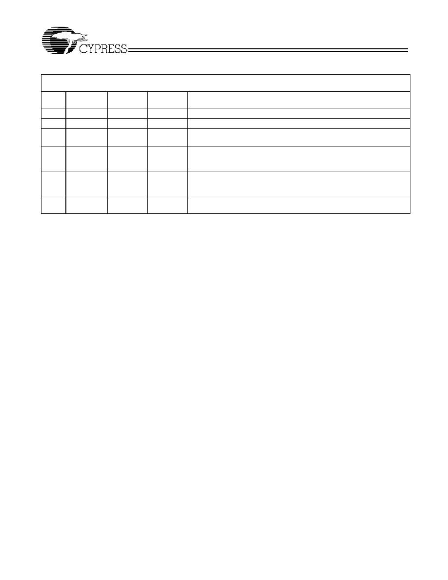
Package Drawing and Dimension
Total Timing Budget, TTB, Spread Aware, and CyberClocks are trademarks of Cypress Semiconductor Corporation. All product
and company names mentioned in this document are the trademarks of their respective holders.
Test Circuits
Ordering Information
Ordering Code
Package Type
Operating Range
CY23FP12OC
28-pin SSOP
Commercial, 0∞C to 70∞C
CY23FP12OCT
28-pin SSOP ≠ Tape and Reel
Commercial,0∞C to 70∞C
CY23FP12OI
28-pin SSOP
Industrial, ≠40∞C to 85∞C
CY23FP12OIT
28-pin SSOP ≠ Tape and Reel
Industrial, ≠40∞C to 85∞C
CY3672
Development Kit
CY3692
CY23FP12S Socket (Label CY3672 ADP006)
Lead-free
CY23FP12OXC
28-pin SSOP
Commercial, 0∞C to 70∞C
CY23FP12OXCT
28-pin SSOP ≠ Tape and Reel
Commercial,0∞C to 70∞C
CY23FP12OXI
28-pin SSOP
Industrial, ≠40∞C to 85∞C
CY23FP12OXIT
28-pin SSOP ≠ Tape and Reel
Industrial, ≠40∞C to 85∞C
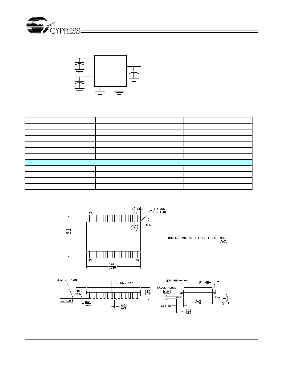
0.1
µ F
V
DD
0.1
µ F
V
DD
CLK
OUT
C
LOAD
OUTPUTS
GND
GND
Test Circuit # 1
Test Circuit for all parameters
28-lead (5.3 mm) Shrunk Small Outline Package O28
51-85079-*C
CY23FP12
Document #: 38-07246 Rev. *E
Page 10 of 10
Document History Page
Document Title: CY23FP12 200-MHz Field Programmable Zero Delay Buffer
Document Number: 38-07246
REV.
ECN NO.
Issue Date
Orig. of
Change
Description of Change
**
115158
07/03/02
HWT
New data sheet
*A
121880
12/14/02
RBI
Power-up requirements added to Absolute Maximum Ratings information
*B
124523
03/19/03
RGL
Final data sheet
Changed title to "200-MHz Field Programmable Zero Delay Buffer"
*C
126938
06/16/03
RGL
Interchanged REF2 in the Pin Configuration diagram
Replaced all divide by 2 default value to divide by 2 in Table 2
Fixed the formula in the Frequency Calculation section
*D
129364
09/10/03
RGL
Changed the CyClocksRT trademark to CyberClocks
Added Note 2 in the TEST mode in Table 3
Added T
LD
specifications in the Switching Characteristics table
*E
299718
See ECN
RGL
Added lead-free devices
Added typical values