FailsafeTM 2.5V/ 3.3V Zero Delay Buffer
CY23FS04
Cypress Semiconductor Corporation
∑
3901 North First Street
∑
San Jose
,
CA 95134
∑
408-943-2600
Document #: 38-07304 Rev. *B
Revised October 12, 2004
Features
∑ Internal DCXO for continuous glitch-free operation
∑ Zero input-output propagation delay
∑ Low-jitter (< 35 ps RMS) outputs
∑ Low Output-to-Output skew (< 200 ps)
∑ 4.17 MHz≠170 MHz reference input
∑ Supports industry standard input crystals
∑ 170 MHz outputs
∑ 5V-tolerant inputs
∑ Phase-locked loop (PLL) Bypass Mode
∑ Dual Reference Inputs
∑ 16-pin TSSOP
∑ 2.5V or 3.3V output power supplies
∑ 3.3V core power supply
∑ Industrial temperature available
Functional Description
The CY23FS04 is a FailSafe
zero delay buffer with two
reference clock inputs and four phase-aligned outputs. The
device provides an optimum solution for applications where
continuous operation is required in the event of a primary clock
failure.
The continuous, glitch-free operation is achieved by using a
DCXO, which serves as a redundant clock source in the event
of a reference clock failure by maintaining the last frequency
and phase information of the reference clock.
The unique feature of the CY23FS04 is that the DCXO is in
fact the primary clocking source, which is synchronized
(phase-aligned) to the external reference clock. When this
external clock is restored, the DCXO automatically resynchro-
nizes to the external clock.
The frequency of the crystal, which will be connected to the
DCXO must be chosen to be an integer factor of the frequency
of the reference clock. This factor is set by two select lines:
S[2:1], please see Table 1. Output power supply, VDD can be
connected to either 2.5V or 3.3V. VDDC is the power supply
pin for internal circuits and must be connected to 3.3V.
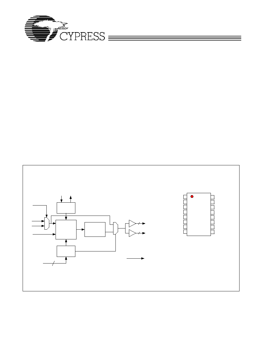
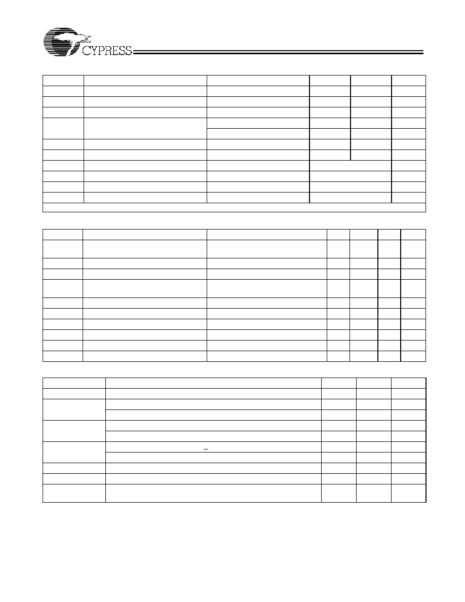
Block Diagram
Pin Configuration
CLKA[1:2]
CLKB[1:2]
DCXO
Decoder
2
Failsafe
TM
Block
PLL
XIN XOUT
2
2
REF2
FBK
S[2:1]
FAIL# /SAFE
REF1
REFSEL
16
15
14
13
12
11
10
9
1
2
3
4
5
6
7
8
CY
23
FS0
4
16 pin TSSOP
REF1
REF2
CLKB1
CLKB2
VSS
VDDC
XIN
S2
REFSEL
FBK
CLKA1
CLKA2
S1
VDD
FAIL#/SAFE
XOUT
CY23FS04
Document #: 38-07304 Rev. *B
Page 2 of 12
FailSafe Function
The CY23FS04 is targeted at clock distribution applications
that could or which currently require continued operation
should the main reference clock fail. Existing approaches to
this requirement have utilized multiple reference clocks with
either internal or external methods for switching between
references. The problem with this technique is that it leads to
interruptions (or glitches) when transitioning from one
reference to another, often requiring complex external circuitry
or software to maintain system stability. The technique imple-
mented in this design completely eliminates any switching of
references to the PLL, greatly simplifying system design.
The CY23FS04 PLL is driven by the crystal oscillator, which is
phase-aligned to an external reference clock so that the output
of the device is effectively phase-aligned to reference via the
external feedback loop. This is accomplished by utilizing a
digitally controlled capacitor array to pull the crystal frequency
over an approximate range of +300 ppm from its nominal
frequency.
Notes:
1. For normal operation, connect either one of the four clock outputs to the FBK input.
2. Weak pull-downs on all outputs
3. Weak pull-ups on these inputs.
4. Weak pull-down on these inputs.
Pin Definition
Pin Number
Pin Name
Description
1,2
REF[1:2]
Reference clock inputs. 5V-tolerant
[4]
.
3,4
CLKB[1:2]
Bank B clock outputs.
[1,2]
14,13
CLKA[1:2]
Bank A clock outputs.
[1,2]
15
FBK
Feedback input to the PLL.
[1,4]
12,5
S[1:2]
Frequency select pins and PLL and DCXO bypass mode.
[3]
8
XIN
Reference crystal input.
9
XOUT
Reference crystal output.
10
FAIL#/SAFE
Valid reference indicator. A high level indicates a valid reference input.
11
VDD
2.5V or 3.3V power supply.
7
VDDC
3.3V power supply.
6
VSS
Ground.
16
REFSEL
Reference select. Selects the active reference clock from either REF1 or REF2. REFSEL
= 1, REF1 is selected, REFSEL = 0, REF2 is selected.
Table 1. Configuration Table
S[2:1]
XTAL (MHz)
REF (MHz)
OUT (MHz)
REF:OUT ratio
REF:XTAL
ratio
Out:XTAL
ratio
Min.
Max.
Min.
Max.
Min.
Max.
00
PLL and DCXO Bypass Mode
01
8.33
30.00
4.17
15.00
4.17
15.00
x1
1/2
1/2
10
8.00
25.00
16.00
50.00
16.00
50.00
x1
2
2
11
8.33
28.33
50.00
170.00
50.00
170.00
x1
6
6
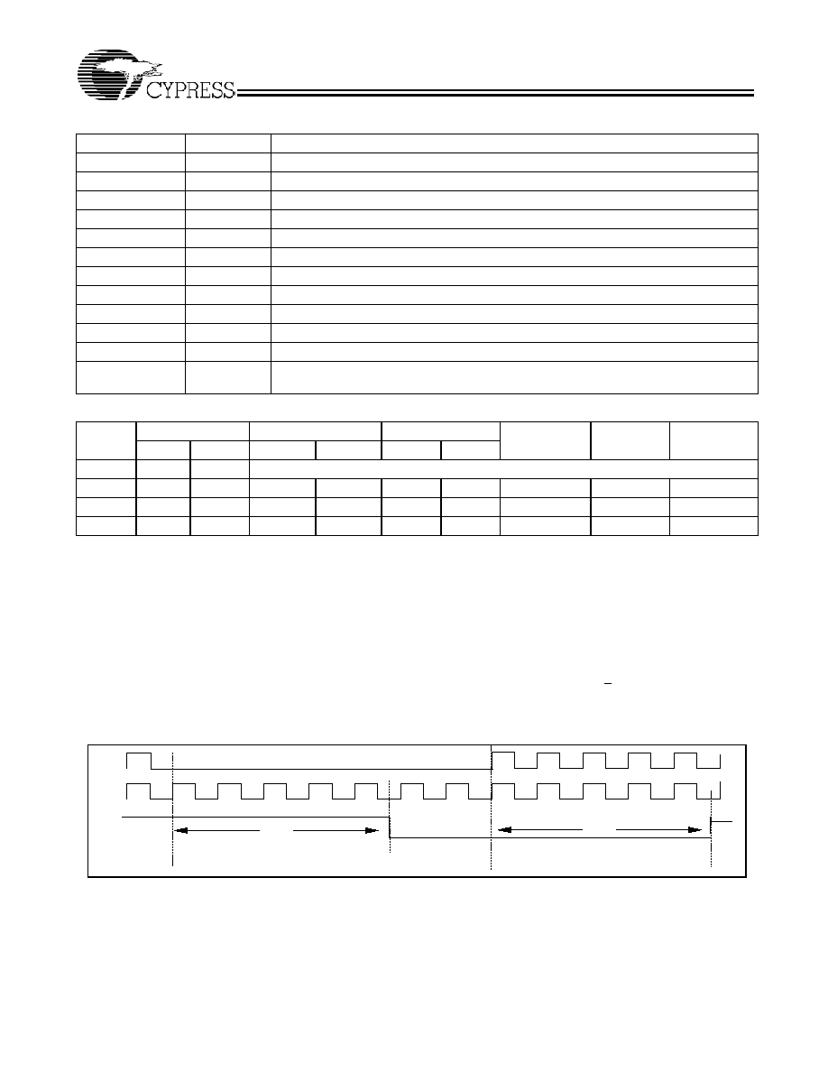
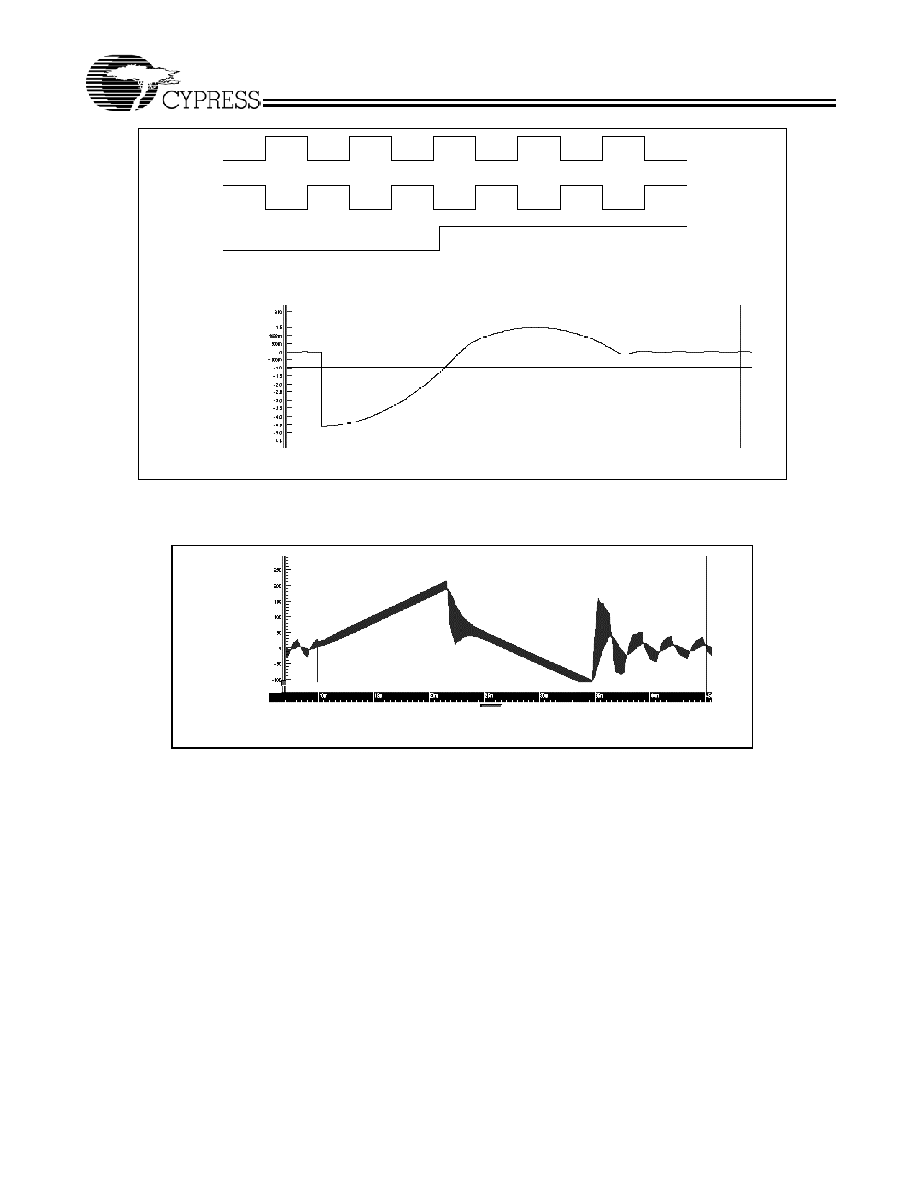
R E F
O U T
F a i l # / S a f e
t
F S L
t
F S H
Figure 1. Fail#/Safe Timing for Input Reference Failing Catastrophically
CY23FS04
Document #: 38-07304 Rev. *B
Page 3 of 12
In this mode, should the reference frequency fail (i.e. stop or
disappear), the DCXO maintains its last setting and a flag
signal (FAIL#/SAFE) is set to indicate failure of the reference
clock.
The CY23FS04 provides 2 select bits, S1 through S2 to control
the reference to crystal frequency ratio. The DCXO is internally
tuned to the phase and frequency of the external reference
only when the reference frequency divided by this ratio is
within the DCXO capture range. If the frequency is out of
range, a flag will be set on the FAIL#/SAFE pin notifying the
system that the selected reference is not valid. If the reference
moves in range, then the flag will be cleared, indicating to the
system that the selected reference is valid.
Table 2. FailSafe Timing Table
Parameter
Description
Conditions
Min.
Max.
Unit
t
FSL
Fail#/Safe Assert Delay
Measured at 80% to 20%, Load = 15 pF
See Figure 2
ns
t
FSH
Fail#/Safe De-assert Delay
Measured at 80% to 20%, Load = 15 pF
See Figure 2
ns
n
=
F
R E F
F
X T A L
= 4
( in a b o v e e x a m p le )
t
F S L ( m a x )
= 2
t
R E F
x n
(
)
+
2 5 n s
t
F S H ( m in )
= 1 2
t
R E F
x n
(
)
+
2 5 n s
Figure 2. Fail#/Safe Timing Formula
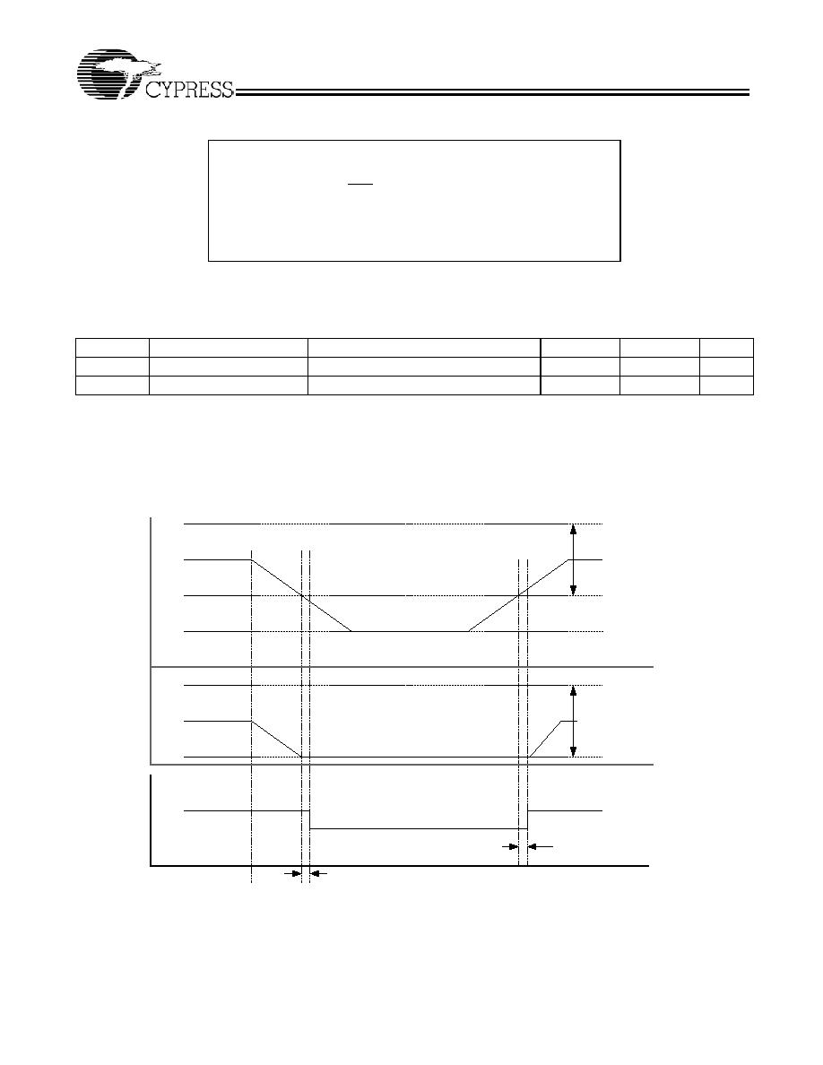
Reference + 300 ppm
Reference - 300 ppm
Reference
Output + 300 ppm
Output - 300 ppm
Output
Fail#/Safe
t
FSH
Reference Off
t
FSL
Time
Freq
u
e
ncy
Volt
Figure 3. FailSafe Timing Diagram: Input Reference Slowly Drifting Out of FailSafe Capture Range
CY23FS04
Document #: 38-07304 Rev. *B
Page 4 of 12
Failsafe typical frequency settling time
Initial valid Ref1=20MHz +100ppm,
then switching to REF2=20MHz
0
50
100
150
0
0.45
1.3
2.5
SETTLING TIME (ms)
O
U
TP
UT FREQ
UENCY DELTA (ppm)
Figure 4. FailSafe Reference Switching Behavior
Figure 5. FailSafe Effective Loop Bandwidth (min)
CY23FS04
Document #: 38-07304 Rev. *B
Page 5 of 12
R E F 1
R E F 2
R E F S E L
0 m s
1 .4 m s
0 d e g
-1 8 0 d e g
0 m s
Figure 6. Sample Timing of Muxing Between Two Reference Clocks 180∞C Out of Phase and
Resulting Output Phase Offset Typical Settling Time (105 MHz)
0 ms
1.4 ms
0
190 fs/cy
190 fsec/cycle = 0.125 mradian/cycle
Figure 7. Resulting Output dphase/Cycle Typical Rate of Change (105 MHz)
CY23FS04
Document #: 38-07304 Rev. *B
Page 6 of 12
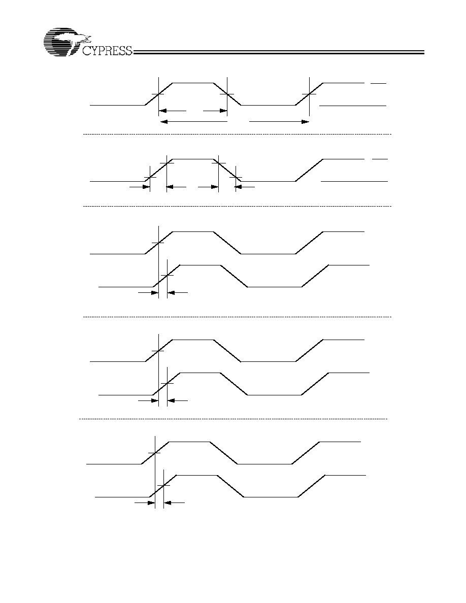
t
1
t
2
D u ty C y c le - t
D C
t
S R (O )
S le w R a te - t
(S R )
V
D D
0 V
2 0 %
8 0 %
8 0 %
2 0 %
V
D D
/2
V
D D
/2
V
D D
/2
V
D D
0 V
O u tp u t-O u tp u t S k e w - t
S K (O )
V
D D
/2
V
D D
/2
t
S K (O )
t
S R (O )
P a rt to P a rt S k e w - t
S K (P P )
F B K ,
P a rt 1
V
D D
/2
t
S K (P P )
V
D D
/2
F B K ,
P a rt 2
S ta tic P h a s e O ffs e t - t
(
)
R E F
V
D D
/2
t
(
)
V
D D
/2
F B K
CY23FS04
Document #: 38-07304 Rev. *B
Page 7 of 12
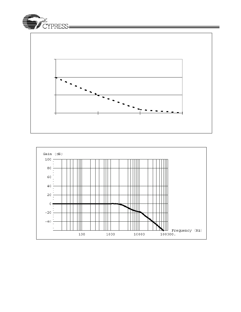
XTAL Selection Criteria and Application Example
Choosing the appropriate XTAL will ensure the FailSafe device
will be able to span an appropriate frequency of operation.
Also, the XTAL parameters will determine the holdover
frequency stability. Critical parameters are as follows. Our
recommendation is to choose:
∑ Low C0/C1 ratio (240 or less) so that the XTAL has enough
range of pullability.
∑ Low temperature frequency variation
∑ Low manufacturing frequency tolerance
∑ Low aging.
C0 is the XTAL shunt capacitance (3 pF ≠ 7 pF typ).
C1 is the XTAL motional capacitance (10 fF ≠ 30 fF typ).
The capacitive load as "seen" by the XTAL is across its
terminals. It is named Clmin (for minimum value), and Clmax
(for maximum value).These are used for calculating the pull
range.
Please note that the Cl range "center" is approximately 20 pF,
but we may not want a XTAL calibrated to that load. This is
because the pullability is not linear, as represented in the
equation above. Plotting the pullability of the XTAL shows this
expected behavior as shown in Figure 8. In this example,
specifying a XTAL calibrated to 14 pF load provides a
balanced ppm pullability range around the nominal frequency.
Note:
5. The above example shows the maximum range the FailSafe internal capacitor array is capable of (0 to 48.6 pF).Cypress recommends the min/max capacitor
array values be programmed to a narrower range such as 6 pF≠30 pF, or 7.5 pF≠27 pF. This ensures the XTAL operates between series resonance and
anti-resonance. Please contact Cypress for choosing these range settings.
Clmin = (12 pF IC input cap + 0 pF pulling cap+ 6 pF trace cap on board)/2 = 9 pF
Clmax = (12 pF IC input cap + 48 pF pulling cap+ 6 pF trace cap on board)/2 = 33 pF
Pull Range =(fClmin≠fClmax)/fClmin = ((C1)/2)[(1/(C0+Clmin))≠(1/(C0+Clmax))]
Pull Range in ppm = ((C1)/2)[(1/(C0+Clmin))≠(1/(C0+Clmax))] ◊ 10
6
Example:
[5]
CY23FS04
Document #: 38-07304 Rev. *B
Page 8 of 12
Calculated value of the pullability range for the XTAL with
C0/C1 ratio of 200, 300 and 400 are shown in Table 3. For this
calculation Cl(min) = 8 pF and Cl(max)= 32 pF has been used.
Using a XTAL that has a nominal frequency specified at load
capacitance of 14 pF, almost symmetrical pullability range has
been obtained.
Next, it is important to calculate the pullability range including
error tolerances. This would be the capture range of the input
reference frequency that the FailSafe device and XTAL combi-
nation would reliably span.
Calculating the capture range involves subtracting error toler-
ances as follows:
Parameter........................................................ f error (ppm)
Manufacturing frequency tolerance ...................................15
Temperature stability ..........................................................30
Aging ................................................................................... 3
Board / trace variation ......................................................... 5
Total ....................................................................................53
Example: Capture Range for XTAL with C0/C1 Ratio of 200
Negative Capture Range= ≠385 ppm + 53 ppm = ≠332 ppm
Positive Capture Range = 333 ppm ≠ 53 ppm = +280 ppm
It is important to note that the XTAL with lower C0/C1 ratio has
wider pullability/capture range as compared to the higher
C0/C1 ratio. This will help the user in selecting the appropriate
XTAL for use in the FailSafe application.
Figure 8. Frequency vs. Cload Behavior for Example XTAL
Pullability Range Vs. Cload
(Normalized to 14pF Cload)
-400.00
-300.00
-200.00
-100.00
0.00
100.00
200.00
300.00
400.00
6
8 10 12 14 16 18 20 22 24 26 28 30 32 34
Cload (pF)
Delta Freq. from nom
C0/C1 = 200
C0/C1 = 300
C0/C1 = 400
Table 3. Pullability Range fro XTAL with Different C0/C1
Ratio
C0/C1 Ratio
Cload(min.) Cload(max.)
Pullability
Range
200
8.0
32.0
≠385 333
300
8.0
32.0
≠256 222
400
8.0
32.0
≠192 166
CY23FS04
Document #: 38-07304 Rev. *B
Page 9 of 12
Absolute Maximum Conditions
Parameter
Description
Condition
Min.
Max.
Unit
V
DD
Supply Voltage
≠0.5
4.6
V
V
IN
Input Voltage
Relative to V
SS
≠0.5
V
DD
+0.5
VDC
T
S
Temperature, Storage
Non Functional
≠65
+150
∞C
T
A
Temperature, Operating Ambient
Commercial Grade
0
70
∞C
Industrial Grade
≠40
85
∞C
T
J
Temperature, Junction
Functional
125
∞C
ESD
HBM
ESD Protection (Human Body Model)
MIL-STD-883, Method 3015
2000
V
ÿ
JC
Dissipation, Junction to Case
Mil-Spec 883E Method 1012.1
29.87
∞C/W
ÿ
JA
Dissipation, Junction to Ambient
JEDEC (JESD 51)
120.11
∞C/W
UL≠94
Flammability Rating
At 1/8 in.
V≠0
MSL
Moisture Sensitivity Level
1
Multiple Supplies: The Voltage on any input or I/O pin cannot exceed the power pin during power-up. Power supply sequencing is NOT required.
Recommended Pullable Crystal Specifications
[6]
Parameter
Name
Comments
Min.
Typ.
Max.
Unit
F
NOM
Nominal crystal frequency
Parallel resonance, fundamental mode,
AT cut
8.00
≠
30.00
MHz
C
LNOM
Nominal load capacitance
≠
14
≠
pF
R
1
Equivalent series resistance (ESR)
Fundamental mode
≠
≠
25
R
3
/R
1
Ratio of third overtone mode ESR to
fundamental mode ESR
Ratio used because typical R
1
values
are much less than the maximum spec
3
≠
≠
DL
Crystal drive level
No external series resistor assumed
≠
0.5
2
mW
F
3SEPLI
Third overtone separation from 3*F
NOM
High side
300
≠
≠
ppm
F
3SEPLO
Third overtone separation from 3*F
NOM
Low side
≠
≠
≠150
ppm
C
0
Crystal shunt capacitance
≠
≠
7
pF
C
0
/C
1
Ratio of shunt to motional capacitance
180
≠
250
C
1
Crystal motional capacitance
14.4
18
21.6
fF
Table 4. Operating Conditions for FailSafe Commercial/Industrial Temperature Devices
Parameter
Description
Min.
Max.
Unit
V
DDC
3.3V Supply Voltage
3.135
3.465
V
V
DD
2.5V Supply Voltage Range
2.375
2.625
V
3.3V Supply Voltage Range
3.135
3.465
V
T
A
Ambient Operating Temperature, Commercial
0
70
∞C
Ambient Operating Temperature, Industrial
≠40
85
∞C
C
L
Output Load Capacitance (Fout < 100 MHz)
30
pF
Output Load Capacitance (Fout > 100 MHz)
15
pF
C
IN
Input Capacitance (except XIN)
7
pF
C
XIN
Crystal Input Capacitance (all internal caps off)
10
13
pF
T
PU
Power-up time for all VDDs to reach minimum specified voltage (power
ramps must be monotonic)
0.05
500
ms
Note:
6. Ecliptek ECX-5788-13.500M, ECX-5807-19.440M, ECX-5872-19.53125M, ECX-5806-18.432M, ECX-5808-27.000M, ECX-5884-17.664M,
ECX-5883-16.384M,ECX-5882-19.200M,ECX-5880-24.576M meet these specifications.
CY23FS04
Document #: 38-07304 Rev. *B
Page 10 of 12
Table 5. Electrical Characteristics for FailSafe Commercial/Industrial Temperature Devices
Parameter
Description
Test Conditions
Min.
Typ.
Max.
Unit
V
IL
Input Low Voltage
CMOS Levels, 30% of V
DD
0.3 ◊ V
DD
V
V
IH
Input High Voltage
CMOS Levels, 70% of V
DD
0.7 ◊ V
DD
V
I
IL
Input Low Current
V
IN
= V
SS
(100k pull-up only)
50
µA
I
IH
Input High Current
V
IN
= V
DD
(100k pull-down only)
50
µA
I
OL
Output Low Current
V
OL
= 0.5V, V
DD
= 2.5V
18
mA
V
OL
= 0.5V, V
DD
= 3.3V
20
mA
I
OH
Output High Current V
OH
= V
DD
≠ 0.5V, V
DD
= 2.5V
18
mA
V
OH
= V
DD
≠ 0.5V, V
DD
= 3.3V
20
mA
I
DDQ
Quiescent Current
All inputs grounded, PLL and DCXO in
bypass mode, Reference Input = 0
250
µA
Table 6. Switching Characteristics for FailSafe Commercial/Industrial Temperature Devices
Parameter
[8]
Description
Test Conditions
Min.
Max.
Unit
f
REF
Reference Frequency
Commercial/Industrial Grades
4.17
170
MHz
f
OUT
Output Frequency
15-pF Load, Commercial/Industrial Grades
4.17
170
MHz
f
XIN
DCXO Frequency
8.0
30
MHz
t
DC
Duty Cycle
Measured at V
DD
/2
47
53
%
t
SR(I)
Input Slew Rate
Measured on REF1 Input, 30% to 70% of V
DD
0.5
4.0
V/ns
t
SR(O)
Output Slew Rate
Measured from 20% to 80% of V
DD
= 3.3V, 15 pF
Load
0.8
4.0
V/ns
Measured from 20% to 80% of V
DD
= 2.5V, 15 pF
Load
0.4
3.0
V/ns
t
SK(O)
Output to Output Skew
All outputs equally loaded, measured at V
DD
/2
200
ps
t
SK(PP)
Part to Part Skew
Measured at V
DD
/2
500
ps
t
(
)
[7]
Static Phase Offset
Measured at V
DD
/2
250
ps
t
D(
)
[7]
Dynamic Phase Offset
Measured at V
DD
/2
200
ps
t
J(CC)
Cycle-to-cycle Jitter
Load = 15 pF, f
OUT
6.25 MHz
200
ps
35
ps
RMS
Ordering Information
Part Number
Package Type
Product Flow
CY23FS04ZI
16-Pin TSSOP
Industrial, ≠40∞C to 85∞C
CY23FS04ZIT
16-Pin TSSOP ≠ Tape and Reel
Industrial, ≠40∞C to 85∞C
CY23FS04ZC
16-Pin TSSOP
Commercial, 0∞C to 70∞C
CY23FS04ZCT
16-Pin TSSOP ≠ Tape and Reel
Commercial, 0∞C to 70∞C
Notes:
7. The
t
(
)
reference feedback input delay is guaranteed for a maximum 4:1 input edge ratio between the two signals as long as
t
SR(I) is maintained.
8. Parameters guaranteed by design and characterization, not 100% tested in production.
9. Includes typical board trace capacitance of 6≠7pF each XIN, XOUT.
CY23FS04
Document #: 38-07304 Rev. *B
Page 11 of 12
© Cypress Semiconductor Corporation, 2004. The information contained herein is subject to change without notice. Cypress Semiconductor Corporation assumes no responsibility for the use
of any circuitry other than circuitry embodied in a Cypress product. Nor does it convey or imply any license under patent or other rights. Cypress products are not warranted nor intended to be
used for medical, life support, life saving, critical control or safety applications, unless pursuant to an express written agreement with Cypress. Furthermore, Cypress does not authorize its
products for use as critical components in life-support systems where a malfunction or failure may reasonably be expected to result in significant injury to the user. The inclusion of Cypress
products in life-support systems application implies that the manufacturer assumes all risk of such use and in doing so indemnifies Cypress against all charges.
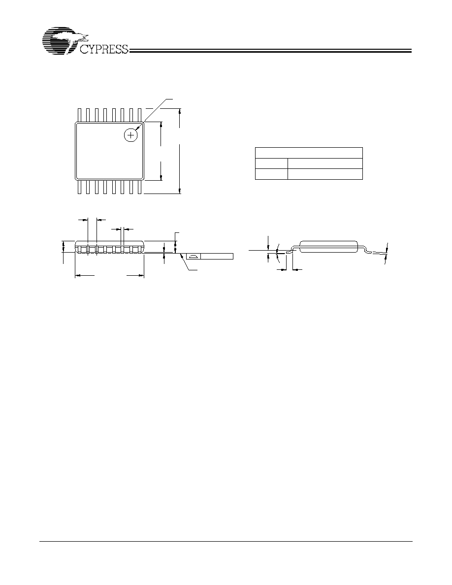
Package Drawing and Dimensions
FailSafe is a trademark of Cypress Semiconductor. All product and company names mentioned in this document are the trade-
marks of their respective holders.
4.90[0.193]
1.10[0.043] MAX.
0.65[0.025]
0.20[0.008]
0.05[0.002]
16
PIN 1 ID
6.50[0.256]
SEATING
PLANE
1
0.076[0.003]
6.25[0.246]
4.50[0.177]
4.30[0.169]
BSC.
5.10[0.200]
0.15[0.006]
0.19[0.007]
0.30[0.012]
0.09[[0.003]
BSC
0.25[0.010]
0∞-8∞
0.70[0.027]
0.50[0.020]
0.95[0.037]
0.85[0.033]
PLANE
GAUGE
DIMENSIONS IN MM[INCHES] MIN.
MAX.
REFERENCE JEDEC MO-153
PACKAGE WEIGHT 0.05 gms
PART #
Z16.173
STANDARD PKG.
ZZ16.173 LEAD FREE PKG.
16-lead TSSOP 4.40 MM Body Z16.173
51-85091-*A
CY23FS04
Document #: 38-07304 Rev. *B
Page 12 of 12
Document History Page
Document Title: CY23FS04 FailsafeTM 2.5V/ 3.3V Zero Delay Buffer
Document #: 38-07304 Rev. *B
REV.
ECN NO. Issue Date
Orig. of
Change
Description of Change
**
123698
04/24/03
RGL
New data sheet
*A
223811
See ECN
RGL/ZJX Changed the XTAL Specifications table.
*B
276712
See ECN
RGL
Removed (T
LOCK
)Lock Time Specification