3.3V Zero Delay Buffer
CY23S08
Cypress Semiconductor Corporation
∑
3901 North First Street
∑
San Jose
∑
CA 95134
∑
408-943-2600
Document #: 38-07265 Rev. *A
Revised December 20, 2002
08
Features
∑ Zero input-output propagation delay, adjustable by
capacitive load on FBK input
∑ Multiple configurations, see Table 2
∑ Multiple low-skew outputs
-- Output-output skew less than 200 ps
-- Device-device skew less than 700 ps
-- Two banks of four outputs, three-stateable by two
select inputs
∑ 10-MHz to 133-MHz operating range
∑ Low jitter, less than 200 ps cycle-cycle (≠1, ≠1H, ≠4)
∑ Advanced 0.65
µ
CMOS technology
∑ Space-saving 16-pin 150-mil SOIC package
∑ 3.3V operation
∑ Spread AwareTM
Functional Description
The CY23S08 is a 3.3V zero delay buffer designed to distribute
high-speed clocks in PC, workstation, datacom, telecom, and
other high-performance applications.
The part has an on-chip PLL which locks to an input clock
presented on the REF pin. The PLL feedback is required to be
driven into the FBK pin, and can be obtained from one of the
outputs. The input-to-output propagation delay is guaranteed
to be less than 350 ps, and output-to-output skew is guaran-
teed to be less than 250 ps.
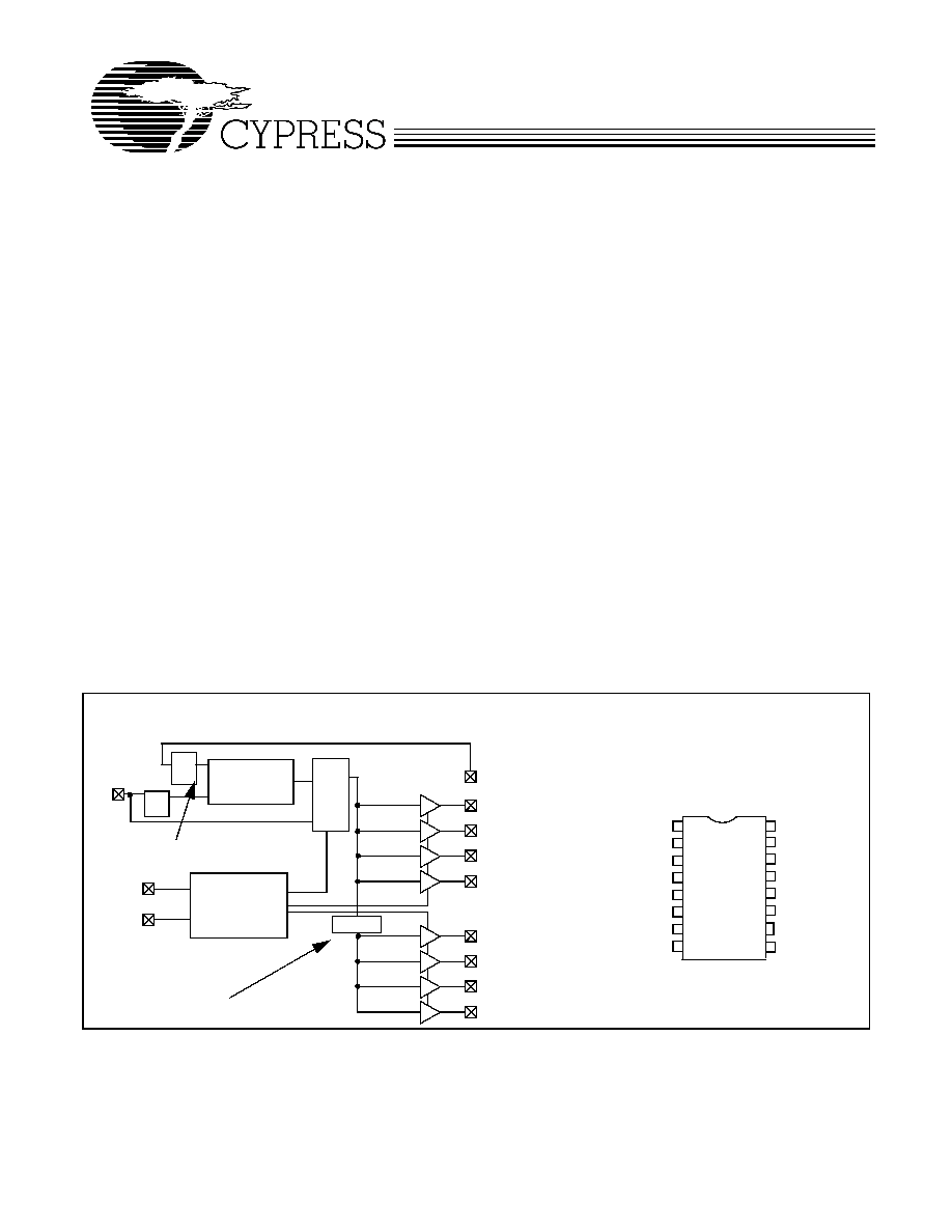
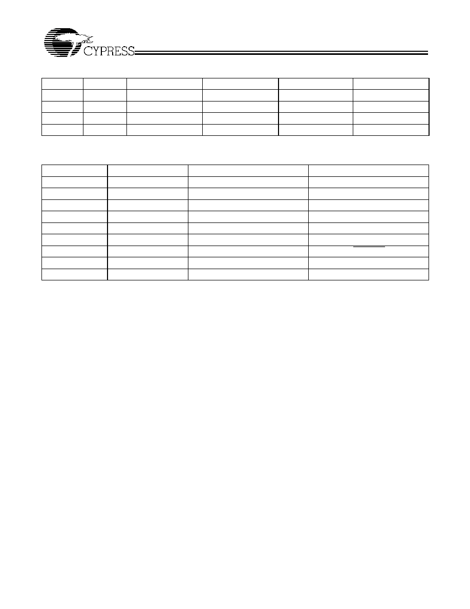
The CY23S08 has two banks of four outputs each, which can
be controlled by the Select inputs as shown in Table 1. If all
output clocks are not required, Bank B can be three-stated.
The select inputs also allow the input clock to be directly ap-
plied to the output for chip and system testing purposes.
The CY23S08 PLL enters a power-down state when there are
no rising edges on the REF input. In this mode, all outputs are
three-stated and the PLL is turned off, resulting in less than
50
µ
A of current draw. The PLL shuts down in two additional
cases as shown in Table 1.
Multiple CY23S08 devices can accept the same input clock
and distribute it in a system. In this case, the skew between
the outputs of two devices is guaranteed to be less than
700 ps.
The CY23S08 is available in five different configurations, as
shown in the Table 2. The CY23S08≠1 is the base part, where
the output frequencies equal the reference if there is no
counter in the feedback path. The CY23S08≠1H is the high-
drive version of the ≠1, and rise and fall times on this device
are much faster.
The CY23S08≠2 allows the user to obtain 2X and 1X frequen-
cies on each output bank. The exact configuration and output
frequencies depends on which output drives the feedback pin.
The CY23S08≠2H is the high-drive version of the ≠2, and rise
and fall times on this device are much faster.
The CY23S08≠3 allows the user to obtain 4X and 2X frequen-
cies on the outputs.
The CY23S08≠4 enables the user to obtain 2X clocks on all
outputs. Thus, the part is extremely versatile, and can be used
in a variety of applications.
9
16
FBK
CLKA4
CLKA3
V
DD
GND
CLKB4
CLKB3
S1
Block Diagram
1
2
3
4
5
6
7
8
10
11
12
13
14
15
REF
CLKA1
CLKA2
V
DD
GND
CLKB1
CLKB2
S2
SOIC
Top View
Pin Configuration
REF
CLKA1
CLKA2
CLKA3
CLKA4
FBK
PLL
MUX
Select Input
Decoding
S2
S1
CLKB1
CLKB2
CLKB3
CLKB4
/2
Extra Divider (≠2, ≠2H, ≠3)
/2
Extra Divider (≠3, ≠4)
2308-1
2308-2
/2
CY23S08
Document #: 38-07265 Rev. *A
Page 2 of 9
Spread AwareTM
Many systems being designed now utilize a technology called
Spread Spectrum Frequency Timing Generation. Cypress
has been one of the pioneers of SSFTG development, and
we designed this product so as not to filter off the Spread
Spectrum feature of the Reference input, assuming it exists.
When a zero delay buffer is not designed to pass the SS fea-
ture through, the result is a significant amount of tracking
skew which may cause problems in systems requiring
synchronization.
For more details on Spread Spectrum timing technology,
please see Cypress's Application Note "EMI Suppression
Techniques with Spread Spectrum Frequency Timing Gener-
ator (SSFTG) ICs."
Table 1. Select Input Decoding.
S2
S1
CLOCK A1≠A4
CLOCK B1≠B4
Output Source
PLL Shutdown
0
0
Three-State
Three-State
PLL
Y
0
1
Driven
Three-State
PLL
N
1
0
Driven
Driven
Reference
Y
1
1
Driven
Driven
PLL
N
Table 2. Available CY23S08 Configurations.
Device
Feedback From
Bank A Frequency
Bank B Frequency
CY2308≠1
Bank A or Bank B
Reference
Reference
CY2308≠1H
Bank A or Bank B
Reference
Reference
CY2308≠2
Bank A
Reference
Reference/2
CY2308≠2H
Bank A
Reference
Reference/2
CY2308≠2
Bank B
2 X Reference
Reference
CY2308≠2H
Bank B
2 X Reference
Reference
CY2308≠3
Bank A
2 X Reference
Reference or Reference
[1]
CY2308≠3
Bank B
4 X Reference
2 X Reference
CY2308≠4
Bank A or Bank B
2 X Reference
2 X Reference
Note:
1.
Output phase is indeterminant (0∞ or 180∞ from input clock). If phase integrity is required, use the CY23S08≠2.
CY23S08
Document #: 38-07265 Rev. *A
Page 3 of 9
Maximum Ratings
Supply Voltage to Ground Potential ............... ≠0.5V to +7.0V
DC Input Voltage (Except Ref)...............≠0.5V to V
DD
+ 0.5V
DC Input Voltage REF ...........................................≠0.5 to 7V
Storage Temperature ................................. ≠65∞C to +150∞C
Max. Soldering Temperature (10 sec.) ........................ 260∞C
Junction Temperature .................................................. 150∞C
Static Discharge Voltage
(per MIL-STD-883, Method 3015) ............................. >2000V
Notes:
2.
Weak pull-down.
3.
Weak pull-down on all outputs.
4.
Weak pull-ups on these inputs.
Pin Description
Pin
Signal
Description
1
REF
[2]
Input reference frequency, 5V tolerant input
2
CLKA1
[3]
Clock output, Bank A
3
CLKA2
[3]
Clock output, Bank A
4
V
DD
3.3V supply
5
GND
Ground
6
CLKB1
[3]
Clock output, Bank B
7
CLKB2
[3]
Clock output, Bank B
8
S2
[4]
Select input, bit 2
9
S1
[4]
Select input, bit 1
10
CLKB3
[3]
Clock output, Bank B
11
CLKB4
[3]
Clock output, Bank B
12
GND
Ground
13
V
DD
3.3V supply
14
CLKA3
[3]
Clock output, Bank A
15
CLKA4
[3]
Clock output, Bank A
16
FBK
PLL feedback input
CY23S08
Document #: 38-07265 Rev. *A
Page 4 of 9
Operating Conditions for CY23S08SC-XX Commercial Temperature Devices
[5.]
Parameter
Description
Min.
Max.
Unit
V
DD
Supply Voltage
3.0
3.6
V
T
A
Operating Temperature (Ambient Temperature)
0
70
∞C
C
L
Load Capacitance, below 100 MHz
30
pF
Load Capacitance, from 100 MHz to 133 MHz
15
pF
C
IN
Input Capacitance
[6]
7
pF
Electrical Characteristics for CY23S08SC-XX Commercial Temperature Devices
Parameter
Description
Test Conditions
Min.
Max
Unit
V
IL
Input LOW Voltage
0.8
V
V
IH
Input HIGH Voltage
2.0
V
I
IL
Input LOW Current
V
IN
= 0V
50.0
µ
A
I
IH
Input HIGH Current
V
IN
= V
DD
100.0
µ
A
V
OL
Output LOW Voltage
[7]
I
OL
= 8 mA (≠1, ≠2, ≠3, ≠4)
I
OL
= 12 mA (-1H, -2H)
0.4
V
V
OH
Output HIGH Voltage
[7]
I
OH
= ≠8 mA (≠1, ≠2, ≠3, ≠4)
I
OH
= ≠12mA (≠1H, ≠2H)
2.4
V
I
DD
(PD mode)
Power Down Supply Current REF = 0 MHz
12.0
µ
A
I
DD
Supply Current
Unloaded outputs, 100-MHz REF,
Select inputs at V
DD
or GND
45.0
mA
70.0
(-1H, -2H)
mA
Unloaded outputs, 66-MHz REF
(≠1,≠2,≠3,≠4)
32.0
mA
Unloaded outputs, 33-MHz REF
(≠1,≠2,≠3,≠4)
18.0
mA
Notes:
5.
Multiple Supplies: The voltage on any input or I/O pin cannot exceed the power pin during power-up. Power supply sequencing is NOT required.
6.
Applies to both Ref Clock and FBK.
7.
Parameter is guaranteed by design and characterization. Not 100% tested in production.
CY23S08
Document #: 38-07265 Rev. *A
Page 5 of 9
Switching Characteristics for CY23S08SC-XX Commercial Temperature Devices
[8]
Parameter
Name
Test Conditions
Min.
Typ.
Max.
Unit
t
1
Output Frequency
30-pF load, All devices
10
100
MHz
t
1
Output Frequency
20-pF load, ≠1H device
10
133.3
MHz
t
1
Output Frequency
15-pF load, ≠1, ≠2, ≠3, ≠4 devices
10
133.3
MHz
Duty Cycle
[7]
= t
2
˜
t
1
(≠1,≠2,≠3,≠4,≠1H, -2H)
Measured at 1.4V, F
OUT
=66.66 MHz
30-pF load
40.0
50.0
60.0
%
Duty Cycle
[7]
= t
2
˜
t
1
(≠1,≠2,≠3,≠4,≠1H, -2H)
Measured at 1.4V, F
OUT
<50.0 MHz
15-pf load
45.0
50.0
55.0
%
t
3
Rise Time
[7]
(≠1, ≠2, ≠3, ≠4)
Measured between 0.8V and 2.0V,
30-pF load
2.20
ns
t
3
Rise Time
[7]
(≠1, ≠2, ≠3, ≠4)
Measured between 0.8V and 2.0V,
15-pF load
1.50
ns
t
3
Rise Time
[7]
(≠1H, -2H)
Measured between 0.8V and 2.0V,
30-pF load
1.50
ns
t
4
Fall Time
[7]
(≠1, ≠2, ≠3, ≠4)
Measured between 0.8V and 2.0V,
30-pF load
2.20
ns
t
4
Fall Time
[7]
(≠1, ≠2, ≠3, ≠4)
Measured between 0.8V and 2.0V,
15-pF load
1.50
ns
t
4
Fall Time
[7]
(≠1H, 2H)
Measured between 0.8V and 2.0V,
30-pF load
1.25
ns
t
5
Output to Output Skew on
same Bank (≠1,≠2,≠3,≠4)
[7]
All outputs equally loaded
200
ps
Output to Output Skew
(≠1H, -2H)
All outputs equally loaded
200
ps
Output Bank A to Output
Bank B Skew (≠1,≠4)
All outputs equally loaded
200
ps
Output Bank A to Output
Bank B Skew (≠2,≠3)
All outputs equally loaded
400
ps
t
6
Delay, REF Rising Edge to
FBK Rising Edge
[7]
Measured at V
DD
/2
0
±
250
ps
t
7
Device to Device Skew
[7]
Measured at V
DD
/2 on the FBK pins of devic-
es
0
700
ps
t
8
Output Slew Rate
[7]
Measured between 0.8V and 2.0V on ≠1H,
-2H device using Test Circuit #2
1
V/ns
t
J
Cycle to Cycle Jitter
[7]
(≠1, ≠1H, ≠4)
Measured at 66.67 MHz, loaded outputs,
15-pF load
200
ps
Measured at 66.67 MHz, loaded outputs,
30-pF load
200
ps
Measured at 133.3 MHz, loaded outputs,
15-pF load
100
ps
t
J
Cycle to Cycle Jitter
[7]
(≠2, -2H, ≠3)
Measured at 66.67 MHz, loaded outputs
30-pF load
400
ps
Measured at 66.67 MHz, loaded outputs
15-pF load
400
ps
t
LOCK
PLL Lock Time
[7]
Stable power supply, valid clocks presented
on REF and FBK pins
1.0
ms
Notes:
8.
All parameters are specified with loaded outputs.
CY23S08
Document #: 38-07265 Rev. *A
Page 6 of 9
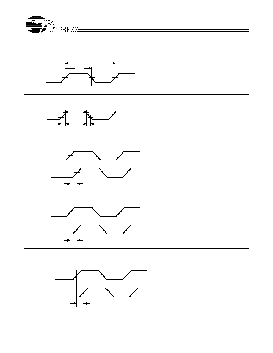
Switching Waveforms
Duty Cycle Timing
t
1
23S08≠3
t
2
1.4V
1.4V
1.4V
All Outputs Rise/Fall Time
23S08≠4
OUTPUT
t
3
3.3V
0V
0.8V
2.0V
2.0V
0.8V
t
4
Output-Output Skew
23S08≠5
1.4V
t
5
OUTPUT
OUTPUT
1.4V
Input-Output Propagation Delay
23S08≠6
V
DD
/2
t
6
INPUT
FBK
V
DD
/2
23S08≠7
V
DD
/2
V
DD
/2
t
7
FBK, Device 1
FBK, Device 2
Device-Device Skew
CY23S08
Document #: 38-07265 Rev. *A
Page 7 of 9
Spread Aware is a trademark of Cypress Semiconductor
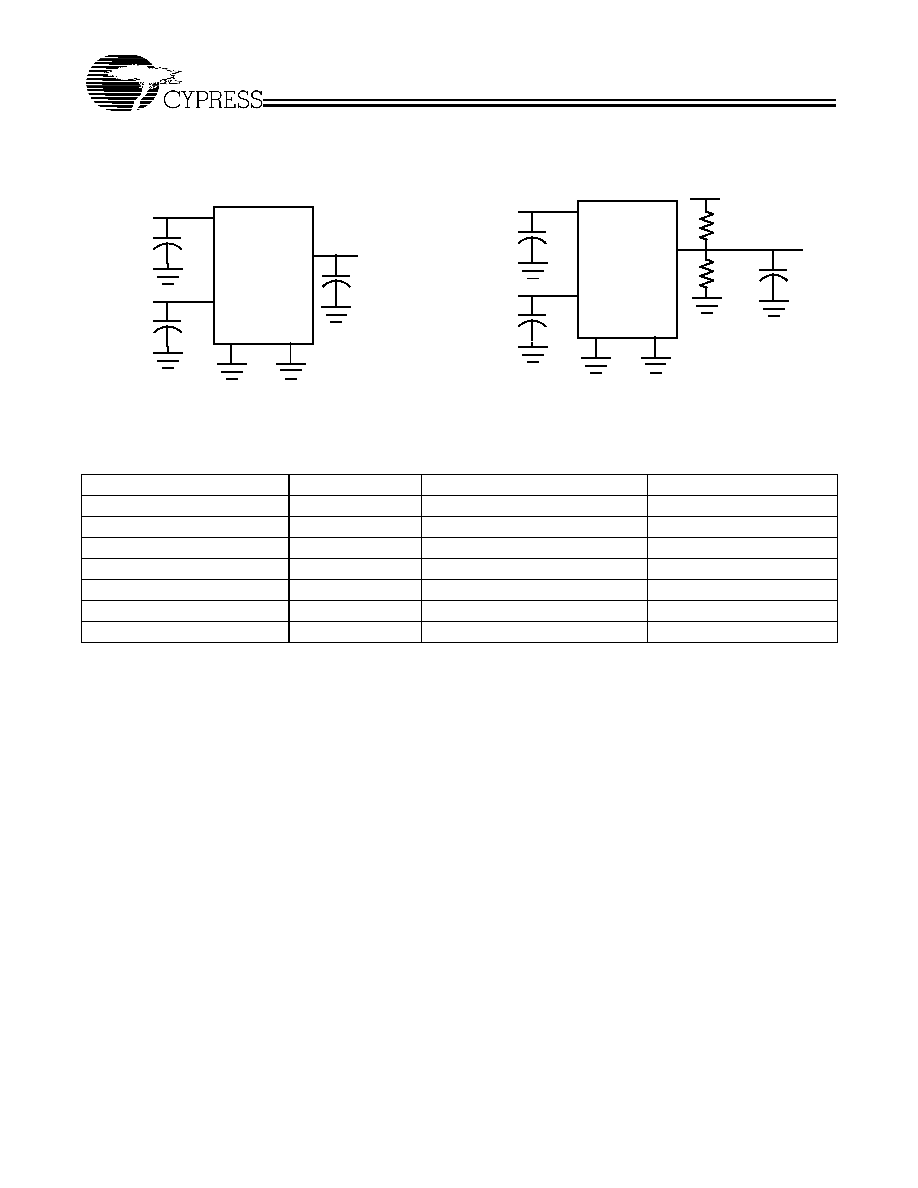
Test Circuits
Ordering Information
Ordering Code
Package Name
Package Type
Operating Range
CY23S08SC≠1
S16
16-pin 150-mil SOIC
Commercial
CY23S08SC≠1H
S16
16-pin 150-mil SOIC
Commercial
CY23S08ZC≠1H
Z16
16-pin 150-mil TSSOP
Commercial
CY23S08SC≠2
S16
16-pin 150-mil SOIC
Commercial
CY23S08SC≠2H
S16
16-pin 150-mil SOIC
Commercial
CY23S08SC≠3
S16
16-pin 150-mil SOIC
Commercial
CY23S08SC≠4
S16
16-pin 150-mil SOIC
Commercial
0.1
µ
F
V
DD
0.1
µ
F
V
DD
CLK
OUT
C
LOAD
OUTPUTS
GND
GND
Test Circuit # 1
V
DD
0.1
µ
F
V
DD
CLK
out
10
pF
OUTPUTS
GND
GND
1 K
1 K
0.1
µ
F
Test Circuit for t
8
, Output slew rate on ≠1H device
Test Circuit for all parameters except t
8
Test Circuit # 2
CY23S08
Document #: 38-07265 Rev. *A
Page 8 of 9
© Cypress Semiconductor Corporation, 2001. The information contained herein is subject to change without notice. Cypress Semiconductor Corporation assumes no responsibility for the use
of any circuitry other than circuitry embodied in a Cypress Semiconductor product. Nor does it convey or imply any license under patent or other rights. Cypress Semiconductor does not authorize
its products for use as critical components in life-support systems where a malfunction or failure may reasonably be expected to result in significant injury to the user. The inclusion of Cypress
Semiconductor products in life-support systems application implies that the manufacturer assumes all risk of such use and in doing so indemnifies Cypress Semiconductor against all charges.
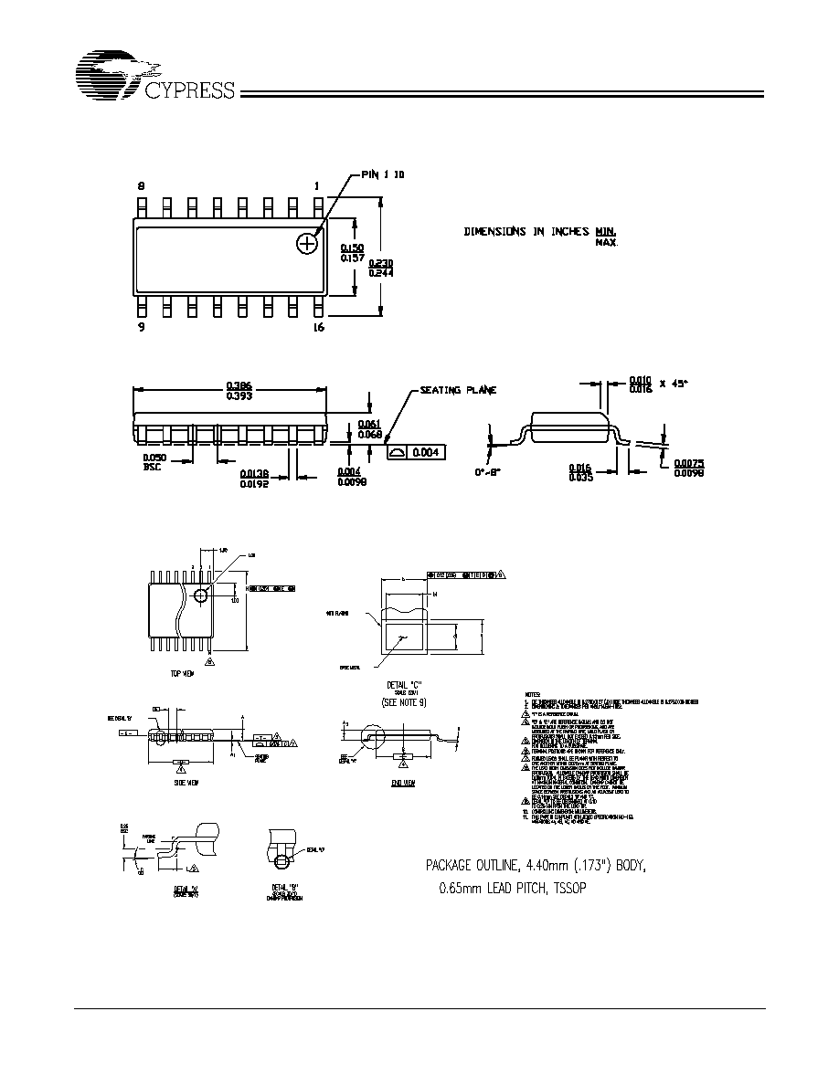
Package Diagrams
16-Lead (150-Mil) Molded SOIC S16
51-85068-A
16-Lead Thin Shrunk Small Outline Package (4.40 MM Body) Z16

CY23S08
Document #: 38-07265 Rev. *A
Page 9 of 9
Document Title: CY23S08 3.3V Zero Delay Buffer
Document Number: 38-07265
REV.
ECN NO.
Issue
Date
Orig. of
Change
Description of Change
**
110530
12/02/01
SZV
Change from Spec number: 38-01107 to 38-07265
*A
122863
12/20/02
RBI
Added power-up requirements to operating conditions information.