 | –≠–ª–µ–∫—Ç—Ä–æ–Ω–Ω—ã–π –∫–æ–º–ø–æ–Ω–µ–Ω—Ç: CY24115-2 | –°–∫–∞—á–∞—Ç—å:  PDF PDF  ZIP ZIP |
MediaClockTM
Mini Disc Clock Generator
CY24115
Cypress Semiconductor Corporation
∑
3901 North First Street
∑
San Jose
∑
CA 95134
∑
408-943-2600
Document #: 38-07275 Rev. *B
Revised December 14, 2002
Features
Benefits
∑ Integrated phase-locked loop (PLL)
High-performance PLL tailored for mini disc applications
∑ Low-jitter, high-accuracy outputs
Meets critical timing requirements in complex system designs
∑ 3.3V operation
Enables application compatibility
∑ 8-pin SOIC package
Industry standard package saves on board space
Part Number
Outputs
Input Frequency Range
Output Frequencies
CY24115-1
1
1 MHz≠30 MHz
45.1584 MHz/90.3168 MHz (selectable)
CY24115-2
1
1 MHz≠30 MHz
90.3168 MHz/180.6336 MHz (selectable)
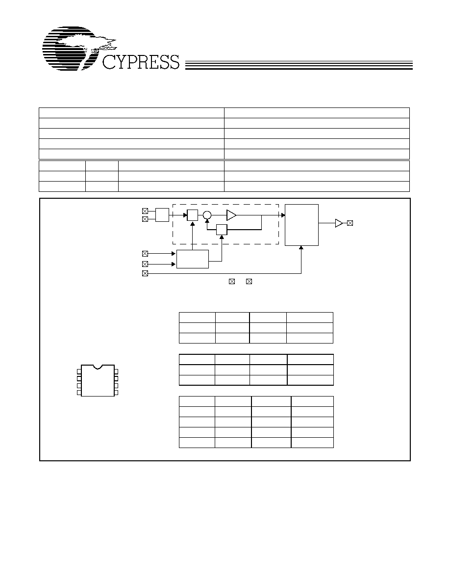
Logic Block Diagram
XIN
XOUT
OUTPUT
DIVIDERS
PLL
OSC
FS0
Q
P
VCO
VDD
VSS
CLKA
FS1
CLKSEL
8-pin SOIC
CY24115
Pin Configurations
1
2
3
4
XOUT
XIN
CLKSEL
CLKA
VSS
FS1
FS0
5
6
7
8
VDD
Table 1. CLKSEL Function CY24115-1
CLKSEL
CLKA
Unit
PPM Error
0
45.1584
MHz
0
1
90.3168
MHz
0
Table 2. CLKSEL Function, CY24115-2
CLKSEL
CLKA
Unit
PPM Error
0
90.3168
MHz
0
1
180.6336
MHz
0
Table 3. Input Frequency Function, CY24115-1 and CY24115-2
FS1
FS0
Xtal Input
Unit
0
0
2.8224
MHz
0
1
5.6448
MHz
1
0
11.2896
MHz
1
1
22.5792
MHz
FREQUENCY
TABLE
CY24115
Document #: 38-07275 Rev. *B
Page 2 of 5
Pin Summary
Pin Name
Pin Number
Pin Description
X
IN
1
Reference input (crystal or external input)
V
DD
2
3.3V voltage supply
CLKSEL
3
CLKA Select Line
For 24115-1, see Table 1 for output values
For 24115-2, see Table 2 for output values
V
SS
4
Ground
CLKA
5
24115-1: 45.1584 MHz/90.3168 MHz (frequency selectable). See Table 1.
24115-2: 90.3168 MHz/180.6336 MHz (frequency selectable). See Table 2.
FS0
6
Input Frequency FS0. See Table 3.
FS1
7
Input Frequency FS1. See Table 3.
X
OUT
[1]
8
Reference Output
Absolute Maximum Conditions
Parameter
Description
Min.
Max.
Unit
V
DD
Supply Voltage
≠0.5
7.0
V
T
S
Storage Temperature
[2]
≠65
125
∞C
T
J
Junction Temperature
125
∞C
Digital Inputs
V
SS
≠ 0.3
V
DD
+ 0.3
V
Digital Outputs Referred to V
DD
V
SS
≠ 0.3
V
DD
+ 0.3
V
Electrostatic Discharge
2
kV
Recommended Operating Conditions
Parameter
Description
Min.
Typ.
Max.
Unit
V
DD
Operating Voltage
3.14
3.3
3.47
V
T
A
Ambient Temperature
0
70
∞C
C
LOAD
Max. Load Capacitance
15
pF
f
REF
Reference Frequency
2.8224
22.5792
MHz
t
1
Driven Reference Edge Rate
0.8
V/ns
DC
IN
Driven Reference Duty Cycle
40
60
%
C
IN
X
IN
, X
OUT
capacitance
12
pF
t
PU
Power-up time for all VDD's to
reach minimum specified voltage
(power ramps must be monotonic)
0.05
500
ms
DC Electrical Characteristics
Parameter
Name
Description
Min.
Typ.
Max.
Unit
I
OH
Output High Current
V
OH
= V
DD
≠ 0.5, V
DD
= 3.3V (source)
12
24
mA
I
OL
Output Low Current
V
OL
= 0.5, V
DD
= 3.3V (sink)
12
24
mA
C
IN
Input Capacitance
CLKSEL, FS0, FS1, excludes XIN, XOUT
7
pF
V
IL
Input Low Voltage
30
% of V
DD
V
IH
Input High Voltage
70
% of V
DD
I
IZ
Input Leakage Current
5
µ
A
I
DD
Supply Current
Sum of Core and Output Current
35
mA
Notes:
1.
Float X
OUT
if X
IN
is externally driven.
2.
Rated for 10 years.
CY24115
Document #: 38-07275 Rev. *B
Page 3 of 5
AC Electrical Characteristics (V
DD
= 3.3V)
Parameter
[3]
Name
Description
Min.
Typ.
Max.
Unit
DC
Output Duty Cycle
Duty Cycle is defined in Figure 1, 50% of V
DD
45
50
55
%
t
3
Rising Edge Slew Rate
Output Clock Rise Time, 20%≠80% of V
DD
0.8
1.4
V/ns
t
4
Falling Edge Slew Rate
Output Clock Fall Time, 80%≠20% of V
DD
0.8
1.4
V/ns
t
9
Clock Jitter
Peak to Peak period jitter
350
ps
t
10
PLL Lock Time
3
ms
Notes:
3.
Not 100% tested.
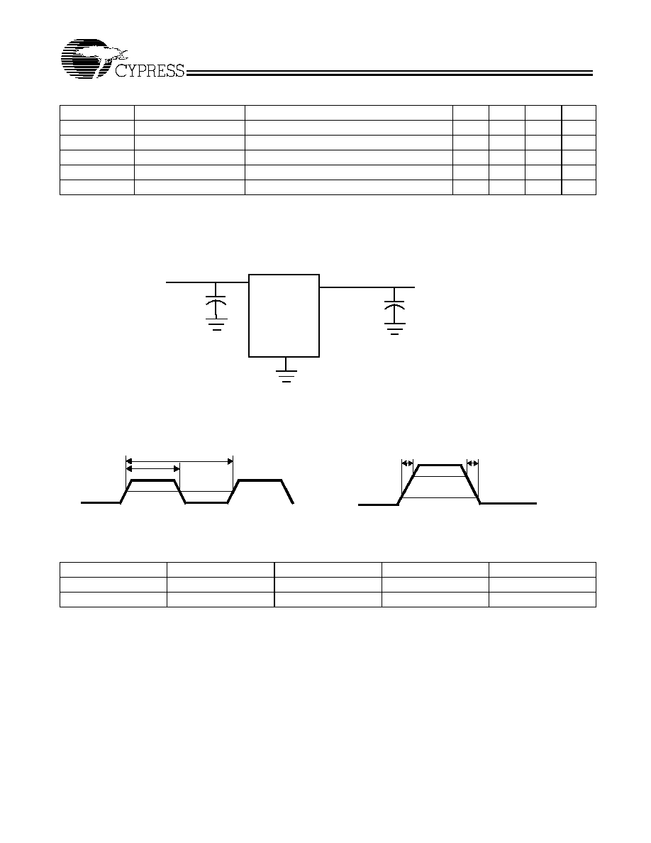
Test Circuit
0.1
µ
F
V
DD
CLK out
C
LOAD
GND
OUTPUTS
t1
t2
CLK
50%
50%
Figure 1. Duty Cycle Definition; DC = t2/t1
t3
CLK
80
20
t4
Figure 2. Rise and Fall Time Definitions
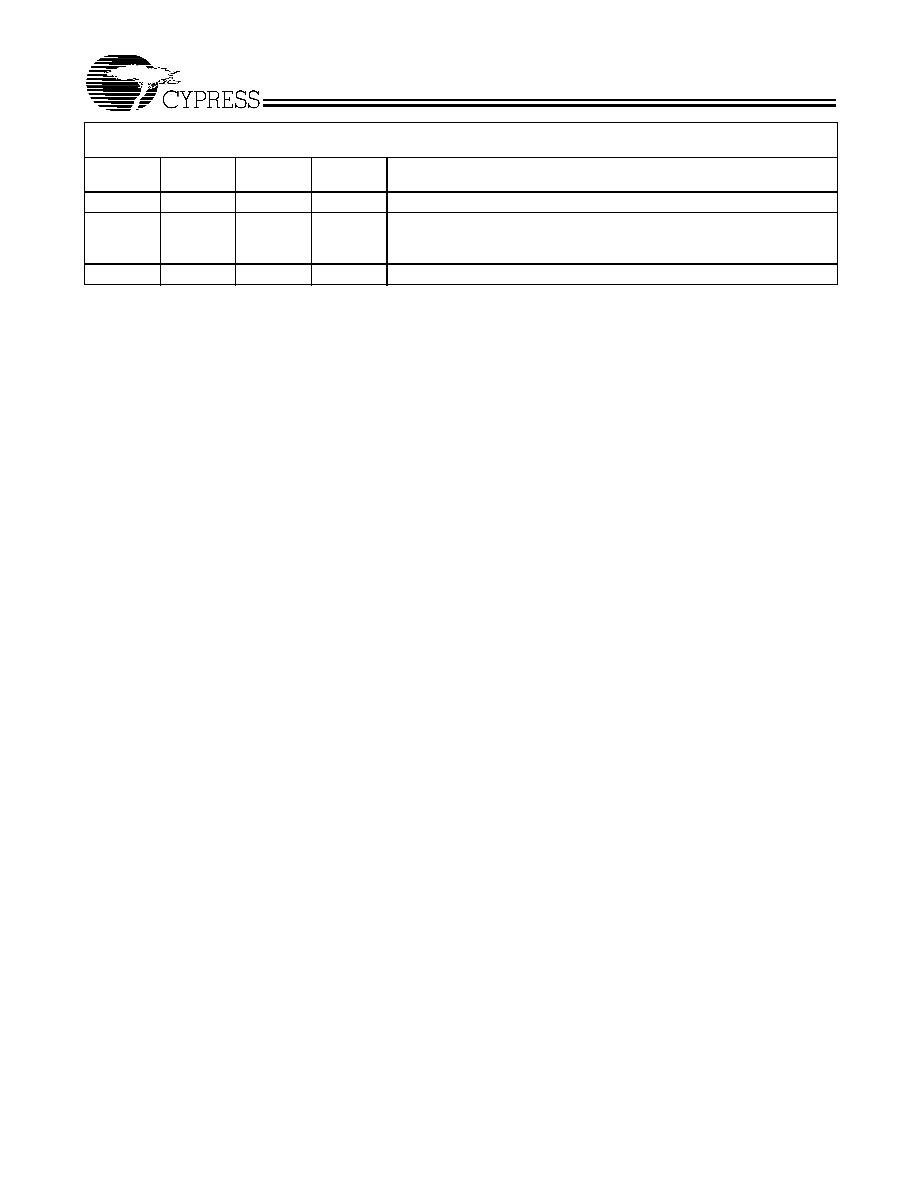
Ordering Information
Ordering Code
Package Name
Package Type
Operating Range
Operating Voltage
CY24115SC-1
S8
8-pin SOIC
Commercial
3.3V
CY24115SC-2
S8
8-pin SOIC
Commercial
3.3V
CY24115
Document #: 38-07275 Rev. *B
Page 4 of 5
© Cypress Semiconductor Corporation, 2002. The information contained herein is subject to change without notice. Cypress Semiconductor Corporation assumes no responsibility for the use
of any circuitry other than circuitry embodied in a Cypress Semiconductor product. Nor does it convey or imply any license under patent or other rights. Cypress Semiconductor does not authorize
its products for use as critical components in life-support systems where a malfunction or failure may reasonably be expected to result in significant injury to the user. The inclusion of Cypress
Semiconductor products in life-support systems application implies that the manufacturer assumes all risk of such use and in doing so indemnifies Cypress Semiconductor against all charges.
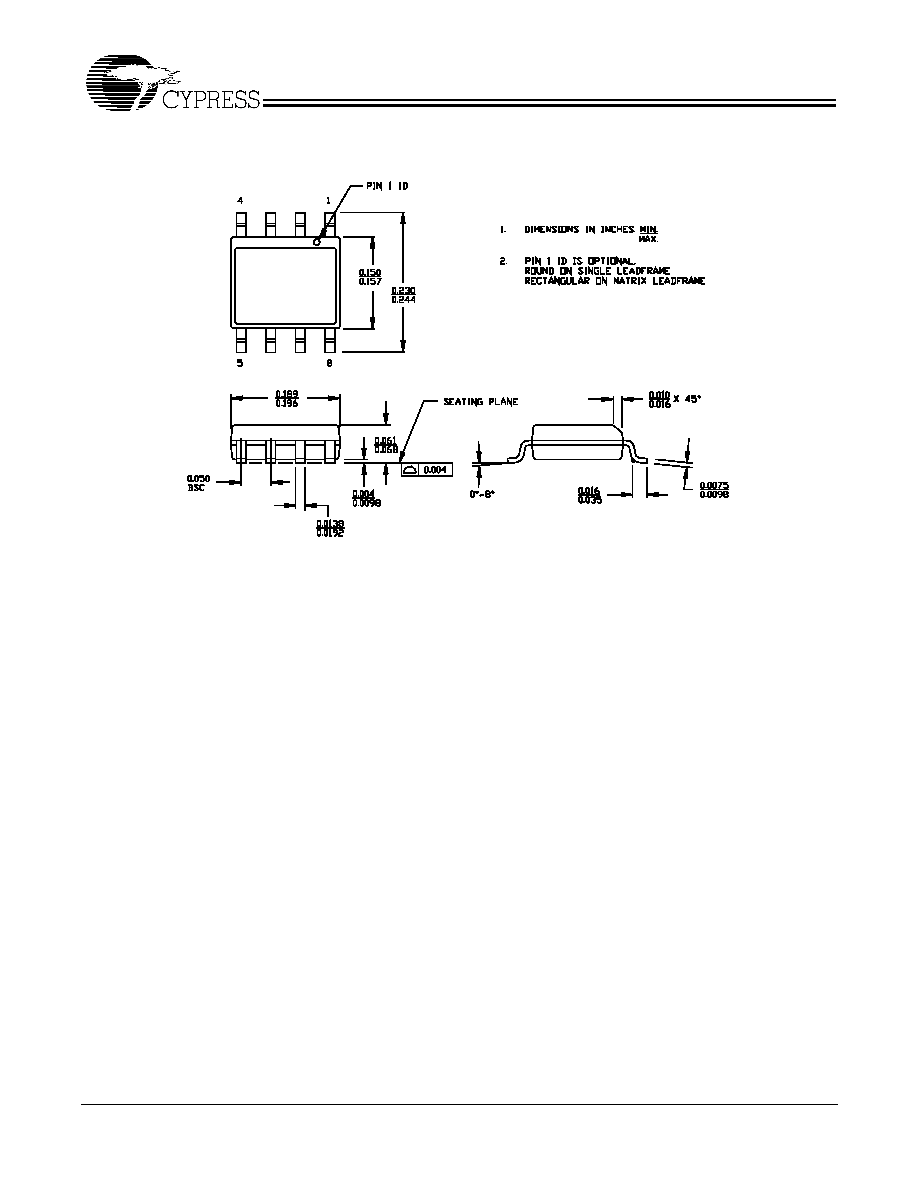
Package Diagram
MediaClock is a trademark of Cypress Semiconductor. All product and company names mentioned in this document are the
trademarks of their respective holders.
8-lead (150-mil) SOIC S8
51-85066-A
CY24115
Document #: 38-07275 Rev. *B
Page 5 of 5
Document Title: CY24115 MediaClockTM Mini Disc Clock Generator
Document Number: 38-07275
REV.
ECN NO.
Issue
Date
Orig. of
Change
Description of Change
**
110767
02/06/02
CKN
New Data Sheet
*A
113515
04/30/02
CKN
Changed from Preliminary to Final
P. 2 in Electrical Characteristics table added (source) to row 1 and (sink) to
row 2
*B
121884
12/14/02
RBI
Power up requirements added to Operating Conditions Information