PRELIMINARY
MediaClockTM 27-MHz VCXO Clock Generator
CY24119
Cypress Semiconductor Corporation
∑
3901 North First Street
∑
San Jose
,
CA 95134
∑
408-943-2600
Document #: 38-07200 Rev. *B
Revised October 8, 2003
Features
∑ Low-jitter, high-accuracy output
∑ VCXO with analog adjust
∑ 3.3V operation
Benefits
∑ Meets critical timing requirements in complex system de-
signs
∑ Large ± 150 ppm range, better linearity
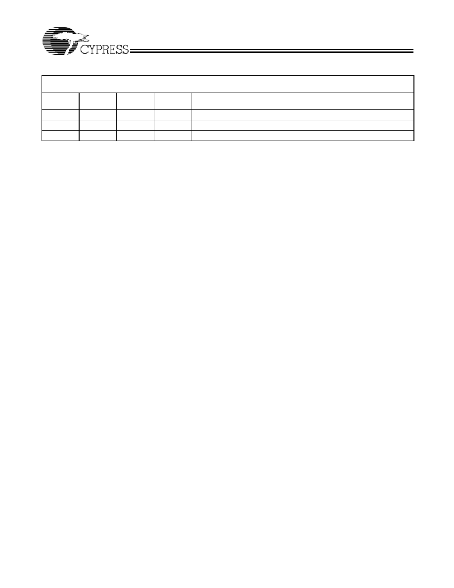
Part Number Outputs
Input Frequency Range
Output Frequencies
CY24119
1
27-MHz pullable crystal per Cypress specification
One copy of 27-MHz (3.3V) positive
slope VCXO curve
CY24119-1
1
27-MHz pullable crystal per Cypress specification
One copy of 27-MHz (3.3V) negative
slope VCXO curve
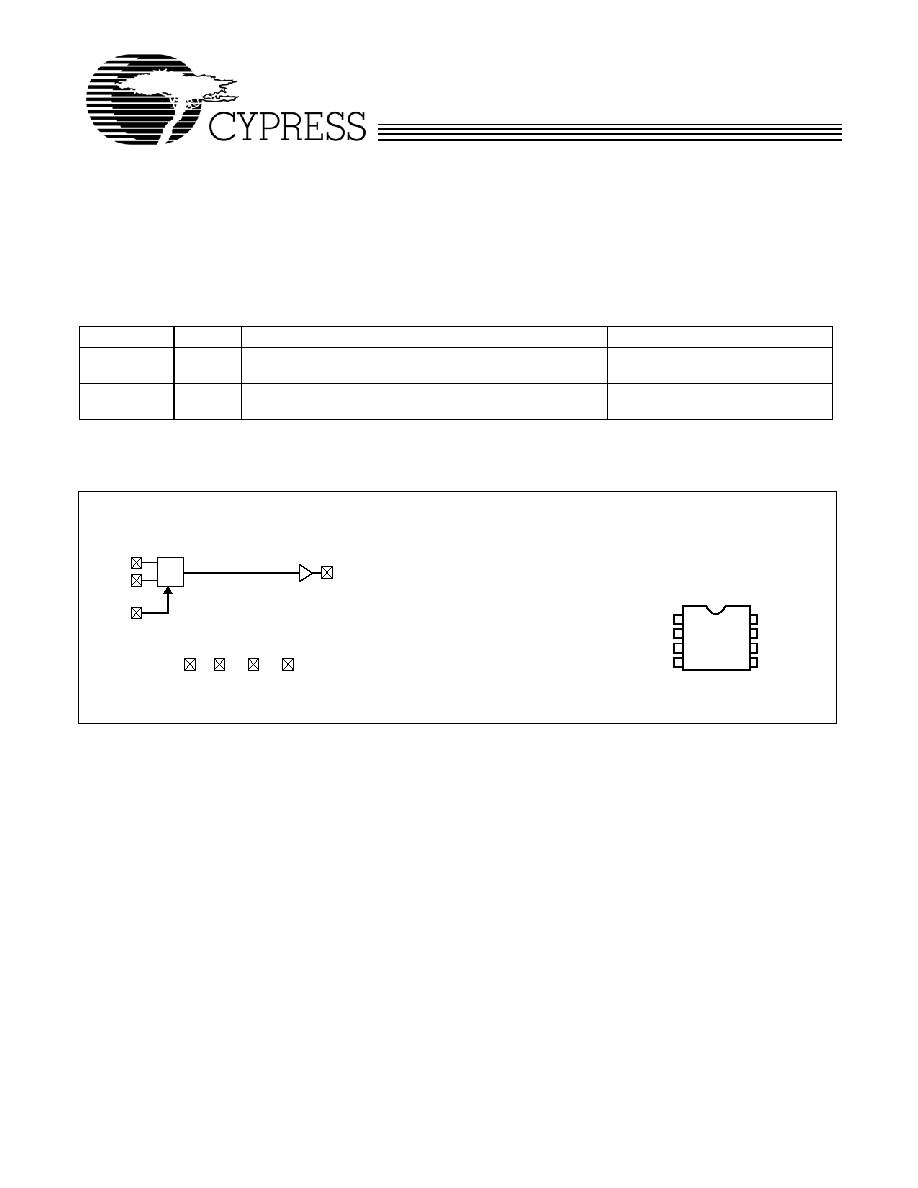
Logic Block Diagram
Pin Configuration
27 XIN
XOUT
27 MHz
OSC
VCXO
VDD
AVSS
AVDD
VSS
8-pin SOIC
CY24119,-1
1
2
3
4
XOUT
XIN
VCXO
27 MHz
AVSS
VSS
VDD
5
6
7
8
AVDD
CY7C09079V/89V/99V
CY7C09179V/89V/99V
PRELIMINARY
CY24119
Document #: 38-07200 Rev. *B
Page 2 of 5
Pin Summary
Name
Pin Number
Description
A
VDD
2
Analog Voltage Supply
V
DD
5
Output Voltage Supply
AV
SS
4
Analog Ground
V
SS
7
Output Ground
X
IN
1
Reference Crystal Input
V
CXO
3
Analog Control for V
CXO
X
OUT
8
Reference Crystal Output
27 MHz
6
27-MHz Clock Output
Absolute Maximum Conditions
Parameter
Description
Min.
Max.
Unit
V
DD
Supply Voltage
≠0.5
7.0
V
T
S
Storage Temperature
[1]
≠65
125
∞C
T
J
Junction Temperature
125
∞C
Electrostatic Discharge
2
kV
Recommended Operating Conditions
Parameter
Description
Min.
Typ.
Max.
Unit
V
DD
, AV
DD
Operating Voltage
3.14
3.3
3.47
V
T
A
Ambient Temperature
0
70
∞ C
C
LOAD
Max Load Capacitance
15
pF
f
REF
Reference Frequency
10
27
30
MHz
t
PU
Power-up time for all VDDs to reach
minimum specified voltage (power
ramps must be monotonic)
0.05
500
ms
DC Electrical Characteristics
Parameter
Name
Description
Min.
Typ.
Max.
Unit
I
OH
Output HIGH Current
V
OH
= V
DD
≠ 0.5, V
DD
= 3.3V (source)
12
24
mA
I
OL
Output LOW Current
V
OL
= 0.5, V
DD
= 3.3V (sink)
12
24
mA
C
IN
Input Capacitance
7
pF
I
IZ
Input Leakage Current
5
µA
f
xo
V
CXO
Pullability Range
≠150
+150
ppm
V
VCXO
V
CXO
Input Range
0
AV
DD
V
f
VBW
V
CXO
Input Bandwidth
DC to 200
kHz
I
DD
Supply Current
Sum of Core and Output Current
13
mA
Pullable Crystal Specifications
Parameter
Description
Condition
Min.
Typ.
Max.
Unit
F
NOM
Nominal crystal frequency
Parallel resonance, funda-
mental mode, AT cut
27
MHz
C
LNOM
Nominal load capacitance
14
pF
R
1
Equivalent series resistance (ESR)
Fundamental mode
25
Note:
1. Not 100% tested.
PRELIMINARY
CY24119
Document #: 38-07200 Rev. *B
Page 3 of 5
R
3
/R
1
Ratio of third overtone mode ESR to fundamen-
tal mode ESR
Ratio used because typical
R
1
values are much less
than the maximum spec.
3
DL
Crystal drive level
No external series resistor
assumed
0.5
2.0
mW
F
3SEPHI
Third overtone separation from 3.F
NOM
High side
300
ppm
F
3SEPLO
Third overtone separation from 3.F
NOM
Low side
≠150
ppm
C
0
Crystal shunt capacitance
7
pF
C
0
/C
1
Ratio of shunt to motional capacitance
180
250
C
1
Crystal motional capacitance
14.4
18
21.6
pF
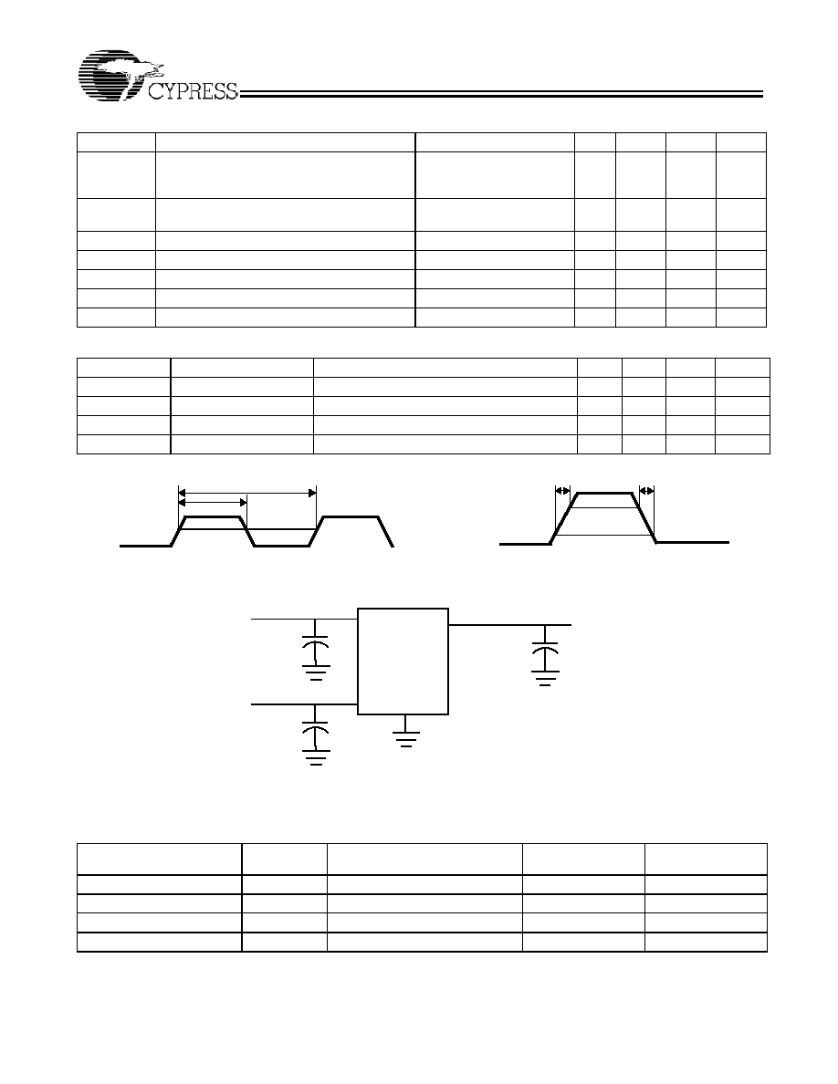
AC Electrical Characteristics
(V
DD
= 3.3V)
Parameter
[1]
Name
Description
Min.
Typ.
Max.
Unit
DC
Output Duty Cycle
Duty Cycle is defined in Figure 1, 50% of V
DD
45
50
55
%
t
3
Rising Edge Slew Rate
Output Clock Rise Time, 20% ≠ 80% of V
DD
0.8
1.4
V/ns
t
4
Falling Edge Slew Rate
Output Clock Fall Time, 80% ≠ 20% of V
DD
0.8
1.4
V/ns
t
9
Clock Jitter
Peak-to-Peak Period Jitter
100
ps
Pullable Crystal Specifications
(continued)
Parameter
Description
Condition
Min.
Typ.
Max.
Unit
50%
Figure 1. Duty Cycle Definition; DC = t
2
/t
1
27 MHz
t1
t2
Figure 2. Rise and Fall Time Definitions
27 MHz
t3
t4
80%
20%
0.1
µF
AV
DD
0.1
µF
V
DD
CLK out
C
LOAD
GND
OUTPUTS
Test Circuit
Ordering Information
Ordering Code
Package
Name
Package Type
Operating Range
Operating Voltage
CY24119SC
S8
8-pin SOIC
Commercial
3.3V
CY24119SCT
S8
8-pin SOIC ≠ Tape and Reel
Commercial
3.3V
CY24119SC-1
S8
8-pin SOIC
Commercial
3.3V
CY24119SC-1T
S8
8-pin SOIC ≠ Tape and Reel
Commercial
3.3V
PRELIMINARY
CY24119
Document #: 38-07200 Rev. *B
Page 4 of 5
© Cypress Semiconductor Corporation, 2003. The information contained herein is subject to change without notice. Cypress Semiconductor Corporation assumes no responsibility for the use
of any circuitry other than circuitry embodied in a Cypress Semiconductor product. Nor does it convey or imply any license under patent or other rights. Cypress Semiconductor does not authorize
its products for use as critical components in life-support systems where a malfunction or failure may reasonably be expected to result in significant injury to the user. The inclusion of Cypress
Semiconductor products in life-support systems application implies that the manufacturer assumes all risk of such use and in doing so indemnifies Cypress Semiconductor against all charges.
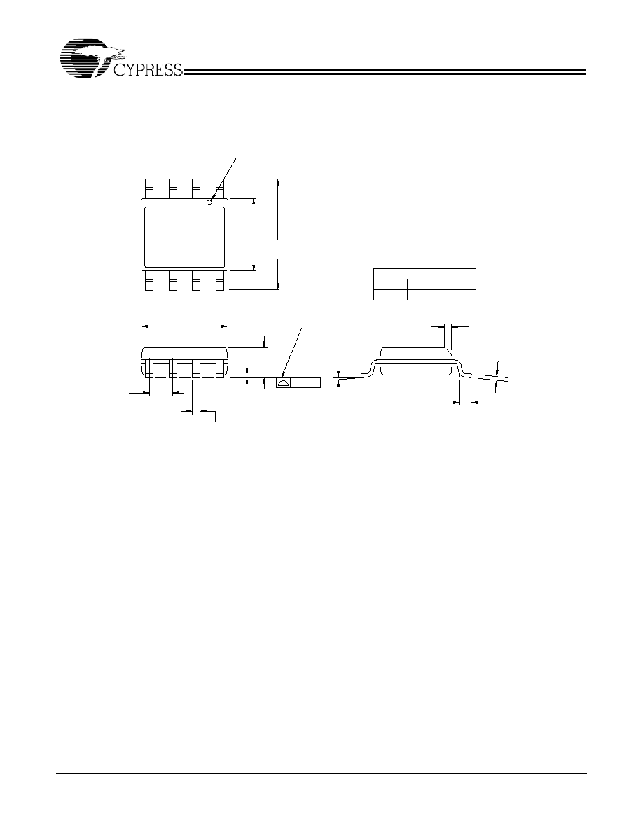
Package Diagram
MediaClock is a trademark of Cypress Semiconductor. All product and company names mentioned in this document may be the
trademarks of their respective holders.
SEATING PLANE
PIN 1 ID
0.230[5.842]
0.244[6.197]
0.157[3.987]
0.150[3.810]
0.189[4.800]
0.196[4.978]
0.050[1.270]
BSC
0.061[1.549]
0.068[1.727]
0.004[0.102]
0.0098[0.249]
0.0138[0.350]
0.0192[0.487]
0.016[0.406]
0.035[0.889]
0.0075[0.190]
0.0098[0.249]
1. DIMENSIONS IN INCHES[MM] MIN.
MAX.
0∞~8∞
0.016[0.406]
0.010[0.254]
X 45∞
2. PIN 1 ID IS OPTIONAL,
ROUND ON SINGLE LEADFRAME
RECTANGULAR ON MATRIX LEADFRAME
0.004[0.102]
8 Lead (150 Mil) SOIC - S08
1
4
5
8
3. REFERENCE JEDEC MS-012
PART #
S08.15 STANDARD PKG.
SZ08.15 LEAD FREE PKG.
4. PACKAGE WEIGHT 0.07gms
8-lead (150-Mil) SOIC S8
51-85066-*C
PRELIMINARY
CY24119
Document #: 38-07200 Rev. *B
Page 5 of 5
Document History Page
Document Title: CY24119 MediaClockTM 27-MHz VCXO Clock Generator
Document Number: 38-07200
REV.
ECN NO. Issue Date
Orig. of
Change
Description of Change
**
111551
03/22/02
CKN
New Data Sheet
*A
121877
12/14/02
RBI
Power-up requirements added to Operating Conditions Information
*B
129724
10/09/03
IJA
Added -1 part, updated Crystal Spec Table