 | ÐлекÑÑоннÑй компоненÑ: CY24130 | СкаÑаÑÑ:  PDF PDF  ZIP ZIP |
Äîêóìåíòàöèÿ è îïèñàíèÿ www.docs.chipfind.ru
HOTLink IITM SMPTE Receiver Training Clock
CY24130
Cypress Semiconductor Corporation
·
3901 North First Street
·
San Jose
,
CA 95134
·
408-943-2600
Document #: 38-07711 Rev. **
Revised February 04, 2005
Features
· Integrated phase-locked loop
· Low-jitter, high-accuracy outputs
· 3.3V operation
Benefits
· Internal PLL with up to 400-MHz internal operation
· Meets critical timing requirements in complex system
designs
· Enables application compatibility
Part Number
Outputs
Input Frequency
Output Frequency Range
CY24130-1
2
27 MHz (Driven Reference)
1 copy 27-MHz reference clock output
1 copy of 27-/36-/54-/148.5-/74.25-MHz (frequency selectable)
CY24130-2
2
27 MHz (Crystal Reference)
1 copy 27-MHz reference clock output
1 copy of 27-/36-/54-/148.5-/74.25-MHz (frequency selectable)
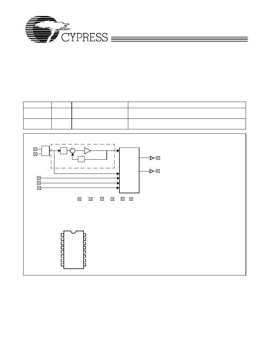
XIN
XOUT
OUTPUT
MULTIPLEXER
AND
DIVIDERS
PLL
OSC.
CLKA
Q
P
VCO
VDDL
AVSS
AVDD
VSS
S0
S1
REFCLK
16-pin TSSOP
1
2
3
4
5
6
7
8
9
10
11
12
13
14
15
16
VSS
VSSL
S1
XIN
XOUT
VDD
S0
AVSS
N/C
S2
REFCLK
AVDD
VDDL
N/C
N/C
CLKA
S2
CY24130-1, -2
Pin Configuration
VDD
VSSL
Logic Block Diagram
CY24130
Document #: 38-07711 Rev. **
Page 2 of 5
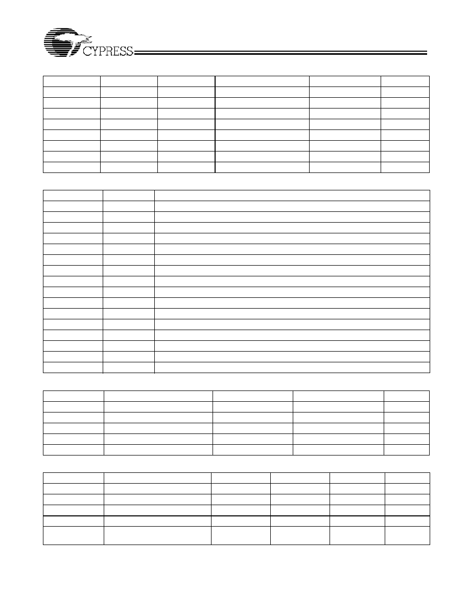
Frequency Select Options
S2
S1
S0
CLKA
REFCLK
Units
0
0
0
27
27
MHz
0
0
1
36
27
MHz
0
1
0
54
27
MHz
0
1
1
148.50
27
MHz
1
0
0
74.25
27
MHz
1
0
1
OFF, pulled low
27
MHz
1
1
0
OFF, pulled low
27
MHz
1
1
1
OFF, pulled low
27
MHz
Pin Description
Name
Pin Number
Description
XIN
1
Reference Crystal Input.
V
DD
2
Voltage Supply.
AV
DD
3
Analog Voltage Supply.
S0
4
Frequency Select 0.
AV
SS
5
Analog Ground.
V
SSL
6
VDDL Ground.
N/C
7
No Connect.
CLKA
8
27-/36-/54-/148.50-/74.25-MHz Clock Output (frequency selectable).
N/C
9
No Connect.
S1
10
Frequency Select 1.
V
DDL
11
Voltage Supply.
N/C 12
No Connect.
VSS
13
Ground.
REFCLK
14
Reference Clock Output.
S2
15
Frequency Select 2.
XOUT
16
Reference Crystal Output. Leave floating for -1.
Absolute Maximum Conditions
Parameter
Description
Min.
Max.
Unit
V
DD,
AV
DD
Supply Voltage
0.5
7.0
V
V
DDL
I/O Supply Voltage
7.0
V
T
J
Junction Temperature
125
°C
Digital Inputs
AV
SS
0.3
AV
DD
+ 0.3
V
Electro-Static Discharge
2
kV
Recommended Operating Conditions
Parameter
Description
Min.
Typ.
Max.
Unit
V
DD
/AV
DDL
/V
DDL
Operating Voltage
3.135
3.3
3.465
V
T
A
Ambient Temperature
0
70
°C
C
LOAD
Max. Load Capacitance
15
pF
f
REF
Reference Frequency
27
MHz
C
LNOM
Nominal Parallel Crystal Load
Capacitance for -2
18
pF
CY24130
Document #: 38-07711 Rev. **
Page 3 of 5
Test and Measurement Set-up
Voltage and Timing Definitions
Note:
1. Not 100% tested.
DC Electrical Specifications
Parameter
[1]
Name
Description
Min.
Typ.
Max.
Unit
I
OH
Output High Current
V
OH
= V
DD
0.5, V
DD
/V
DDL
= 3.3V
12
24
mA
I
OL
Output Low Current
V
OL
= 0.5, V
DD
/V
DDL
= 3.3V
12
24
mA
I
IH
Input High Current
V
IH
= V
DD
5
10
µA
I
IL
Input Low Current
V
IL
= 0V
10
µA
V
IH
Input High Voltage
CMOS levels, 70% of V
DD
0.7
V
V
IL
Input Low Voltage
CMOS levels, 30% of V
DD
0.3
V
I
VDD
Supply Current
AV
DD
/V
DD
Current
16
mA
I
VDDL
Supply Current
V
DDL
Current
14
mA
AC Electrical Specifications
Parameter
[1]
Name
Description
Min.
Typ.
Max.
Unit
DC
Output Duty Cycle
Duty Cycle is defined in Figure 1; t
1
/t
2
, 50% of
V
DD
45
50
55
%
ER
Rising Edge Rate
Output Clock Edge Rate, Measured from 20% to
80% of V
DD
, C
LOAD
= 15 pF. See Figure 2.
0.8
1.4
V/ns
EF
Falling Edge Rate
Output Clock Edge Rate, Measured from 80% to
20% of V
DD
, C
LOAD
= 15 pF. See Figure 2.
0.8
1.4
V/ns
t
9
Clock Jitter
CLKA Peak-Peak Period Jitter
100
ps
t
10
PLL Lock Time
3
ms
0.1
µF
V
DDs
Outputs
C
LOAD
GND
DUT
Clock
Output
V
DD
50% of V
DD
0V
t
1
t
2
Figure 1. Duty Cycle Definitions
CY24130
Document #: 38-07711 Rev. **
Page 4 of 5
© Cypress Semiconductor Corporation, 2005. The information contained herein is subject to change without notice. Cypress Semiconductor Corporation assumes no responsibility for the use
of any circuitry other than circuitry embodied in a Cypress product. Nor does it convey or imply any license under patent or other rights. Cypress products are not warranted nor intended to be
used for medical, life support, life saving, critical control or safety applications, unless pursuant to an express written agreement with Cypress. Furthermore, Cypress does not authorize its
products for use as critical components in life-support systems where a malfunction or failure may reasonably be expected to result in significant injury to the user. The inclusion of Cypress
products in life-support systems application implies that the manufacturer assumes all risk of such use and in doing so indemnifies Cypress against all charges.
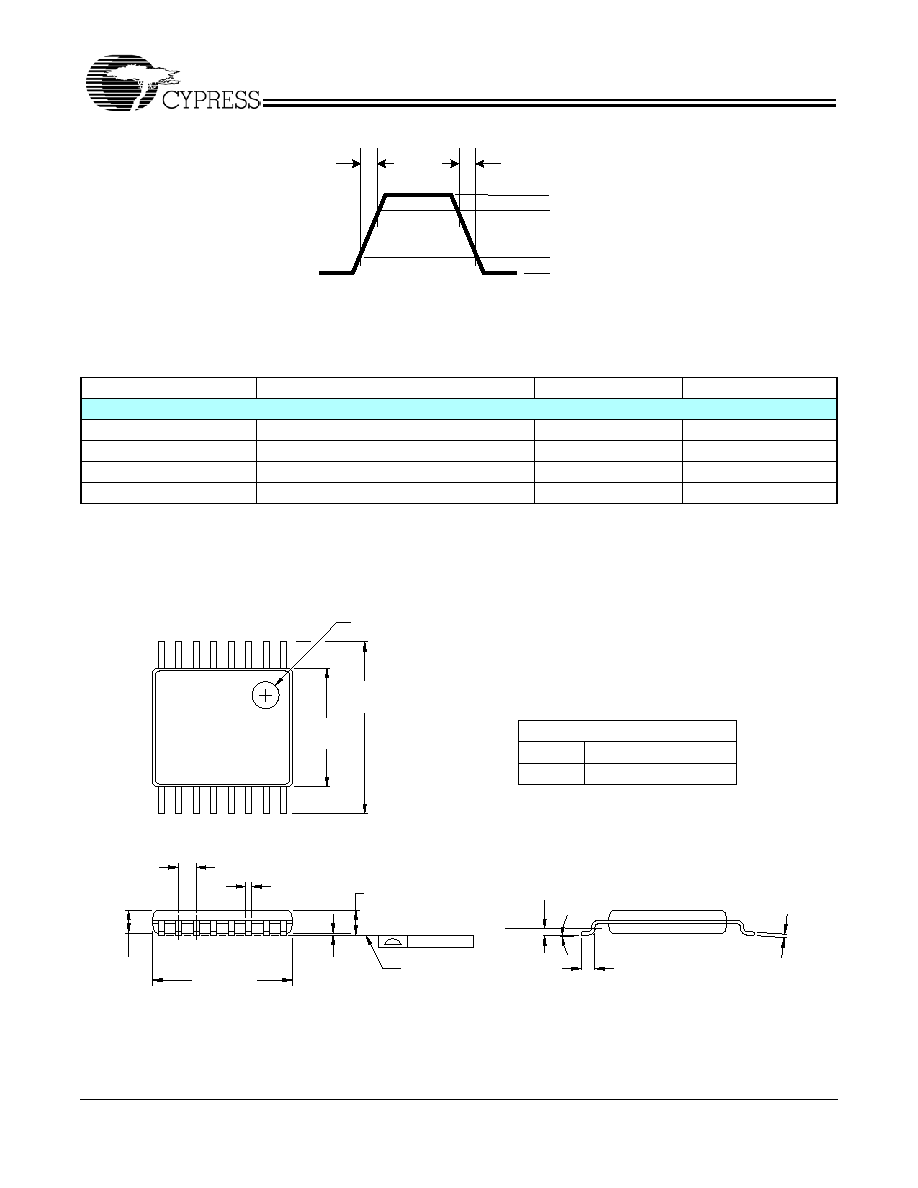
Package Drawing and Dimensions
MediaClock is a trademark of Cypress Semiconductor Corporation. All product and company names mentioned in this document
may be the trademarks of their respective holders.
Ordering Information
Ordering Code
Package Type
Operating Range
Operating Voltage
Lead-free
CY24130ZXC-1
16-Pin TSSOP
Commercial
3.3V
CY24130ZXC-1T
16-Pin TSSOP Tape and Reel
Commercial
3.3V
CY24130ZXC-2
16-Pin TSSOP
Commercial
3.3V
CY24130ZXC-2T
16-Pin TSSOP Tape and Reel
Commercial
3.3V
Clock
Output
t
3
t
4
V
DD
80% of V
DD
20% of V
DD
0V
Figure 2. ER = (0.6 x V
DD
) /t
3
, EF = (0.6 x V
DD
) /t
4
4.90[0.193]
1.10[0.043] MAX.
0.65[0.025]
0.20[0.008]
0.05[0.002]
16
PIN 1 ID
6.50[0.256]
SEATING
PLANE
1
0.076[0.003]
6.25[0.246]
4.50[0.177]
4.30[0.169]
BSC.
5.10[0.200]
0.15[0.006]
0.19[0.007]
0.30[0.012]
0.09[[0.003]
BSC
0.25[0.010]
0°-8°
0.70[0.027]
0.50[0.020]
0.95[0.037]
0.85[0.033]
PLANE
GAUGE
DIMENSIONS IN MM[INCHES] MIN.
MAX.
REFERENCE JEDEC MO-153
PACKAGE WEIGHT 0.05 gms
PART #
Z16.173
STANDARD PKG.
ZZ16.173 LEAD FREE PKG.
16-lead TSSOP 4.40 MM Body Z16.173
51-85091-*A

CY24130
Document #: 38-07711 Rev. **
Page 5 of 5
Document History Page
Document Title: CY24130 HOTLink IITM SMPTE Receiver Training Clock
Document Number: 38-07711
REV.
ECN NO. Issue Date
Orig. of
Change
Description of Change
**
314514
See ECN
RGL
New Data Sheet