 | –≠–ª–µ–∫—Ç—Ä–æ–Ω–Ω—ã–π –∫–æ–º–ø–æ–Ω–µ–Ω—Ç: CY2413-1 | –°–∫–∞—á–∞—Ç—å:  PDF PDF  ZIP ZIP |
Set Top Box
Clock Generator with VCXO
CY2413
Cypress Semiconductor Corporation
∑
3901 North First Street
∑
San Jose
∑
CA 95134
∑
408-943-2600
Document #: 38-07226 Rev. *A
Revised December 14, 2002
Features
Benefits
∑ Low jitter, high accuracy outputs
Meets critical timing requirements in complex system designs
∑ VCXO with analog adjust
Large ±150 ppm range, better linearity
∑ 3.3V Operation with 2.5 V Output Option
Enables application compatibility
Part Number
Outputs
Input Frequency Range
Output Frequency Range
CY2413-1
3
13.5-MHz pullable Crystal per
Cypress Specification
13.5-, 27-, 36-, and 54-MHz selectable output frequencies
CY2413-2
2
13.5-MHz pullable Crystal per
Cypress Specification
27-, and 54-MHz output frequencies
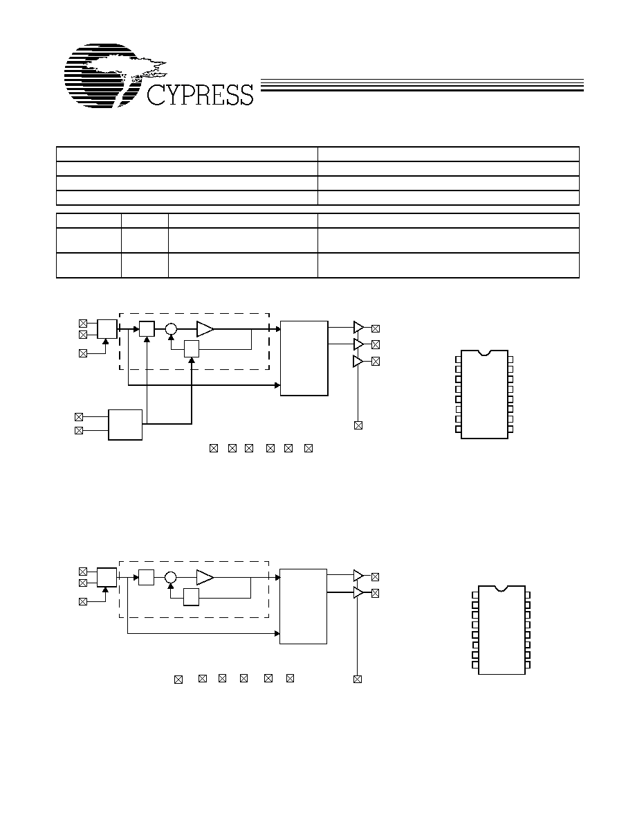
Logic Block Diagram CY2413-1
XIN
XOUT
LCLK_1
PLL
ROM
OSC
LCLK_2
Q
P
VCO
AVDD
VSS
VCXO
VDDL VSSL
VDD AVSS
FS0
FS1
Output
Multiplexer
and
Dividers
OE
XIN
XOUT
LCLK_1
PLL
OSC
LCLK_2
Q
P
VCO
AVDD
VSS
VCXO
VDDL
VSSL
VDD
AVSS
Output
Multiplexer
and
Dividers
OE
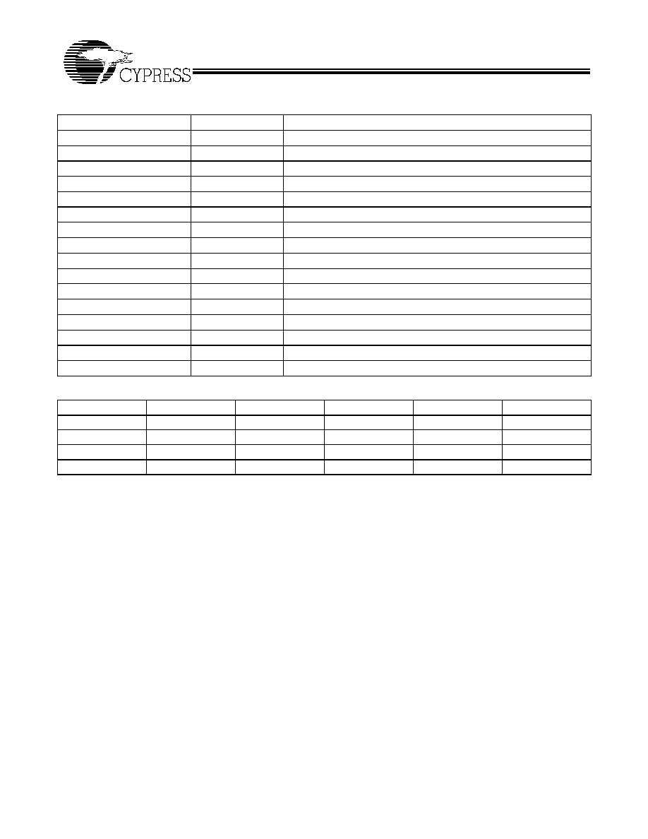
Logic Block Diagram CY2413-2
CLK_3
Pin Configuration
16-pin TSSOP
CY2413-1
1
2
3
4
5
6
7
8
9
10
11
12
13
14
15
16
VDDL
VSSL
VCXO
LCLK_2
NC
LCLK_1
FS0
XOUT
CLK_3
XIN
VDD
OE
FS1
VSS
AVDD
AVSS
16-pin TSSOP
CY2413-2
1
2
3
4
5
6
7
8
9
10
11
12
13
14
15
16
VDDL
VSSL
VCXO
LCLK_2
NC
LCLK_1
NC
XOUT
NC
XIN
VDD
OE
NC
VSS
AVDD
AVSS
Pin Configuration
CY2413
Document #: 38-07226 Rev. *A
Page 2 of 8
Pin Summary - CY2413-1
Name
Pin Number
Description
XIN
1
Reference Crystal Input
V
DD
2
Voltage Supply
A
VDD
3
Analog Voltage Supply
VCXO
4
Input Analog control voltage for VCXO
AV
SS
5
Analog Ground
V
SSL
6
LCLK Ground
FS1
7
Frequency Select
OE
8
Output Enable
LCLK_1
9
Configurable Clock output 1 at VDDL level
FS0
10
Frequency Select
VDDL
11
LCLK Voltage Supply (2.5V or 3.3V)
LCLK_2
12
Configurable Clock output 2 at VDDL level
VSS
13
Ground
NC
14
No Connect
CLK_3
15
Configurable Clock output 3
XOUT
[1]
16
Reference Crystal Output
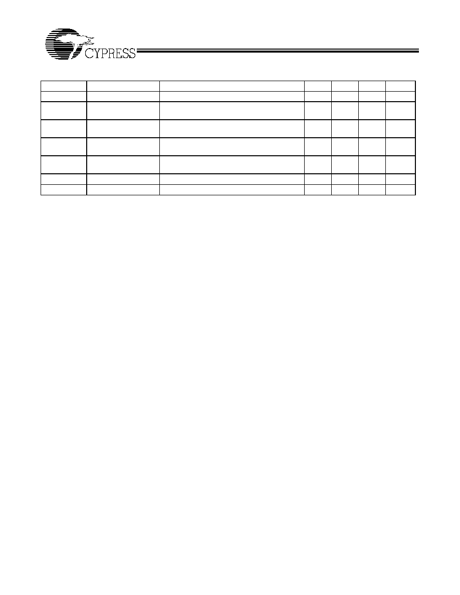
Frequency Select Table - CY2413-1
FS1
FSO
Input
LCLK_1
LCLK_2
CLK_3
0
0
13.5
54
36
off
0
1
13.5
13.5
36
13.5
1
0
13.5
27
54
13.5
1
1
13.5
27
27
13.5
Note:
1.
Float XOUT if XIN is externally driven
CY2413
Document #: 38-07226 Rev. *A
Page 3 of 8
Pin Summary≠ CY2413-2
Pullable Crystal Specifications
Absolute Maximum Conditions
Name
Pin Number
Description
XIN
1
Reference Crystal Input
V
DD
2
Voltage Supply
AV
DD
3
Analog Voltage Supply
VCXO
4
Input Analog control voltage for VCXO
AV
SS
5
Analog Ground
V
SSL
6
LCLK Ground
NC
7
No Connect
OE
8
Output Enable
LCLK_1
9
54-MHz Clock output 1 at VDDL level
NC
10
No Connect
V
DDL
11
LCLK Voltage Supply (2.5V or 3.3V)
LCLK_2
12
27-MHz Clock output 2 at VDDL level
V
SS
13
Ground
NC
14
No Connect
NC
15
No Connect
XOUT
[1]
16
Reference Crystal Output
Parameter
Name
Min.
Typ.
Max.
Unit
CR
load
Crystal Load Capacitance
14
pF
C0/C1
240
ESR
Equivalent Series Resistance
35
T
o
Operating Temperature
0
70
∞C
Crystal Accuracy
Crystal Accuracy
+ 20
ppm
TT
s
Stability over temperature and aging
+ 50
ppm
Parameter
Description
Min.
Max.
Unit
V
DD
Supply Voltage
≠0.5
7.0
V
V
DDL
I/O Supply Voltage
≠0.5
7.0
V
T
S
Storage Temperature
[2]
≠65
100
∞C
T
J
Junction Temperature
125
∞C
Digital Inputs
AV
SS
≠ 0.3
AV
DD
+ 0.3
V
Digital Outputs referred to V
DD
V
SS
≠ 0.3
V
DD
+ 0.3
V
Digital Outputs referred to V
DDL
V
SSL
≠ 0.3
V
DDL
+0.3
V
Analog Input referred to AV
DD
AV
SS
≠ 0.3
AV
DD
+ 0.3
V
Electro-Static Discharge
2
kV
Soldering Temperature 10 sec
235∞
∞C
Note:
2.
Rated for 10 years.
CY2413
Document #: 38-07226 Rev. *A
Page 4 of 8
Recommended Operating Conditions
DC Electrical Characteristics
Parameter
Description
Min.
Typ.
Max.
Unit
V
DD
Operating Voltage
3.0
3.3
3.6
V
V
DDL
Operating Voltage
2.375
2.5
2.625
V
AV
DD
Analog Operating Voltage
3.0
3.3
3.6
V
T
A
Ambient Temperature
0
70
∞C
C
LOAD
Max. Load Capacitance
V
DD
/V
DDL
=3.3V
15
pF
C
LOAD
Max. Load Capacitance
V
DDL
=2.5V
15
pF
f
REF
Reference Frequency
13.5
MHz
P
max
Max. Output Power Dissipation
115
∞C/W
t
PU
Power-up time for all VDD's to
reach minimum specified voltage
(power ramps must be
monotonic)
0.05
500
ms
Parameter
[3]
Name
Description
Min.
Typ.
Max.
Unit
I
OH
Output High Current
V
OH
= V
DD
≠ 0.5, V
DD
/V
DDL
= 3.3V
12
24
mA
I
OL
Output Low Current
V
OL
= 0.5, V
DD
/V
DDL
= 3.3V
12
24
mA
I
OH
Output High Current
V
OH
= V
DDL
≠ 0.5, V
DDL
= 2.5V
8
16
mA
I
OL
Output Low Current
V
OL
= 0.5, V
DDL
= 2.5V
8
16
mA
V
IH
Input High Voltage
CMOS levels, 70% of V
DD
0.7
VDD
V
IL
Input Low Voltage
CMOS levels, 30% of V
DD
0.3
VDD
C
IN
Input Capacitance
Frequency Select and OE Pins
7
pF
I
IZ
Input Leakage Current
Frequency Select and OE Pins
5
µ
A
f
XO
VCXO pullability range
≠150
+150
ppm
V
VCXO
VCXO input range
0
AV
DD
V
f
VBW
VCXO input bandwidth
DC to 200
kHz
I
VDD
Supply Current
AV
DD
/V
DD
Current
10
35
mA
I
VDDL3
Supply Current
V
DDL
Current (V
DDL
=3.6V)
5
15
mA
I
VDDL2
Supply Current
V
DDL
Current (V
DDL
=2.625V)
5
12
mA
CY2413
Document #: 38-07226 Rev. *A
Page 5 of 8
AC Electrical Characteristics
Parameter
[3]
Name
Description
Min.
Typ.
Max.
Unit
DC
Output Duty Cycle
Duty Cycle is defined in Figure 2, 50% of V
DD
45
50
55
%
t
3
Rising Edge Rate
Output Clock Rise Time, 80% ≠ 20% of
V
DD
/V
DDL
, V
DDL
= 3.3V
0.8
1.4
V/ns
t
3
Rising Edge Rate
Output Clock Rise Time, 80% ≠ 20% of
V
DDL
= 2.5V
0.6
1.2
V/ns
t
4
Falling Edge Rate
Output Clock Fall Time, 80% ≠ 20% of
V
DD
/V
DDL
, V
DDL
= 3.3V
0.8
1.4
V/ns
t
4
Falling Edge Rate
Output Clock Fall Time, 80% ≠ 20% of
V
DDL
= 2.5V
0.6
1.2
V/ns
t
9
Clock Jitter
Peak to Peak period jitter
250
450
ps
t
10
PLL Lock Time
Measured from V
DD
= 3.0V
3
ms
Note:
3.
Not 100% tested