PRELIMINARY
MediaClockTM
Graphics Clock Generator
CY24141-3
Cypress Semiconductor Corporation
∑
3901 North First Street
∑
San Jose
∑
CA 95134
∑
408-943-2600
Document #: 38-07324 Rev. **
Revised April 4, 2002
Features
Benefits
∑ Integrated phase-locked loop (PLL)
High-performance PLL tailored for multimedia applications
∑ Low-jitter, high-accuracy output
Meets critical timing requirements in complex system designs
∑ 3.3V operation with 2.5V/1.68V output
Enables application compatibility
∑ Ultra-linear crystal capacitors
Ensures 0PPM Accuracy
Part Number
Outputs
Input Frequency Range
Output Frequencies
CY24141-3
2
18.432 MHz
18.432 MHz, 53.94605395 MHz/54 MHz (selectable)
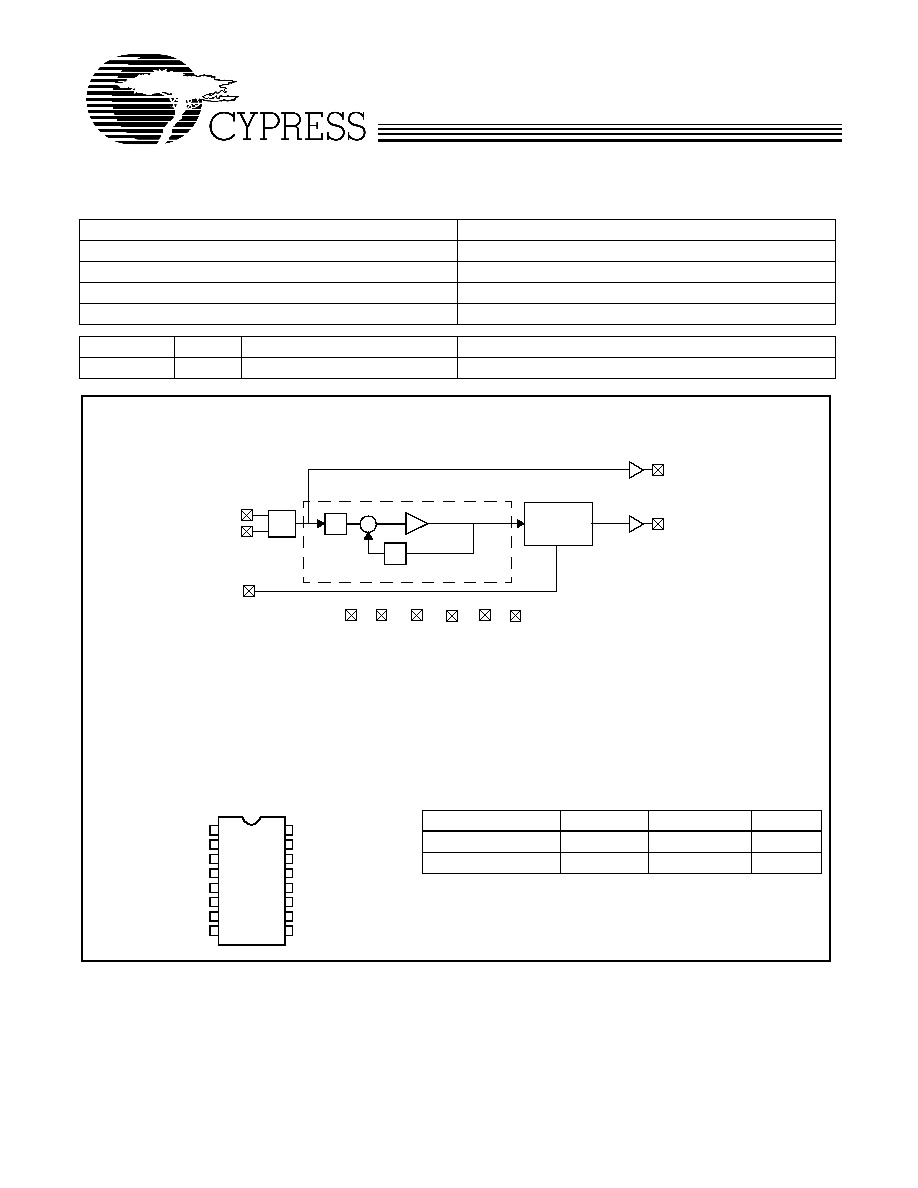
Logic Block Diagram
XIN
XOUT
CLK_B (selectable)
OUTPUT
DIVIDER
PLL
OSC
Q
P
VCO
VDDL
AVSS
AVDD
VSSL
FS
VDD
VSS
CLK_A 18.432 MHz
16-pin TSSOP
CY24141ZC-3
1
2
3
4
5
6
7
8
9
10
11
12
13
14
15
16
VSS
VSSL
N/C
N/C
XIN
XOUT
VDD
FS
AVSS
CLK_B
N/C
CLK_A
N/C
AVDD
VDDL
N/C
Pin Configurations
CY24141 Frequency Select Table
Frequency Select
PPM
CLK_B
Unit
1
≠1.000073
53.94605395
MHz
0
0
54
MHz
PRELIMINARY
CY24141-3
Document #: 38-07324 Rev. **
Page 2 of 6
Pin Summary
Absolute Maximum Conditions
Recommended Operating Conditions
Pin Name
Pin Number
Pin Description
X
IN
1
Reference Input
V
DD
2
Voltage Supply
AV
DD
3
Analog Voltage Supply
FS
4
Frequency Select Pin (Internal Pull-down Resistor)
AV
SS
5
Analog Ground
V
SSL
6
Output Ground
N/C
7
No Connect
N/C
8
No Connect
CLK_B
9
53.94605395-MHz/54-MHz Clock Output (Frequency Selectable) @ V
DDL
level
N/C
10
No Connect
V
DDL
11
Output Voltage Supply for CLK_B
N/C
12
No Connect
V
SS
13
Ground
N/C
14
No Connect
CLK_A
15
18.432-MHz Clock Output
XOUT
[1]
16
Reference Output
Parameter
Description
Min.
Max.
Unit
AVDD
Supply Voltage
≠0.5
7.0
V
T
S
Storage Temperature
[2]
≠65
125
∞C
T
J
Junction Temperature
125
∞C
Digital Inputs
V
SS
≠ 0.3
V
DD
+ 0.3
V
Digital Outputs referred to V
DD
V
SS
≠ 0.3
V
DD
+ 0.3
V
Electrostatic Discharge
2000
V
Parameter
Description
Min.
Typ.
Max.
Unit
AVDD
Analog Voltage Supply
3.15
3.45
3.6
V
VDD
Voltage Supply
3.15
3.45
3.6
V
VDDL
H
2.5V Output Voltage Supply
2.25
2.5
2.75
V
VDDL
L
1.68V Output Voltage Supply
1.63
1.68
1.75
V
T
A
Ambient Temperature
0
85
∞C
C
LOAD
Max Load Capacitance
15
pF
f
REF
Reference Frequency
18.432
MHz
Note:
1.
Float X
OUT
if X
IN
is externally driven.
2.
Rated for 10 years.

PRELIMINARY
CY24141-3
Document #: 38-07324 Rev. **
Page 3 of 6
DC Electrical Characteristics
Parameter
Description
Conditions
Min.
Typ.
Max.
Unit
I
OH3.3
Output High Current
V
OH
= V
DD
≠ 0.5, V
DD
= 3.3 V
12
24
mA
I
OL3.3
Output Low Current
V
OL
= 0.5, V
DD
= 3.3 V
12
24
mA
I
OH2.5
Output High Current
V
OH
= V
DDL
≠ 0.5, V
DDL
= 2.5 V
8
20
mA
I
OL2.5
Output Low Current
V
OL
= 0.5, V
DDL
= 2.5 V
8
20
mA
I
OH1.68
Output High Current
V
OH
= V
DDL
≠ 0.5, V
DDL
= 1.68 V
6
12
mA
I
OL1.68
Output Low Current
V
OL
= 0.5, V
DDL
= 1.68 V
6
12
mA
V
IH
Input High Voltage
FS Frequency Select Input
70%
V
DD
V
IL
Input Low Voltage
FS Frequency Select Input
30%
V
DD
R
I
Input Resistor
FS Frequency Select Pull Down Resistor
80
100
135
kohm
C
IN
Input Capacitance
7
pF
X
LDCAP
Crystal Load Capacitance
Internal Load Caps
12.9
pF
I
IZ
Input Leakage Current
5
10
µ
A
I
DD
Supply Current
Sum of Core and Output Current
30
35
mA
Cycle-Cycle Jitter Specifications (V
DD
= 3.15V≠3.6V)
Parameter
Description
Conditions
1
Typ.
Max.
Unit
t
9
Clock Jitter≠peak-peak
Cycle-Cycle Jitter≠18.432 MHz
12
55
140
ps
t
9
Clock Jitter≠peak-peak
Cycle-Cycle Jitter≠54 MHz
V
DDL
= 1.63V≠1.75V
32
135
220
ps
t
9
Clock Jitter≠peak-peak
Cycle-Cycle Jitter≠54 MHz
V
DDL
= 2.25V≠2.75V
11
70
150
ps
t
9
Clock Jitter≠peak-peak
Cycle-Cycle Jitter≠53.94605395 MHz
V
DDL
= 1.63V≠1.75V
31
160
220
ps
t
9
Clock Jitter≠peak-peak
Cycle-Cycle Jitter≠53.94605395 MHz
V
DDL
= 2.25V≠2.75V
11
70
150
ps
1000-cycle Jitter (V
DD
= 3.15V≠3.6V)
Parameter
Description
Conditions
1
Typ.
Max.
Unit
t
10
Clock Jitter≠peak-peak
1000-Cycle-Cycle Jitter≠18.432 MHz
19
95
140
ps
t
10
Clock Jitter≠peak-peak
1000-Cycle-Cycle Jitter≠54 MHz
V
DDL
= 1.63V≠1.75V
55
275
400
ps
t
10
Clock Jitter≠peak-peak
1000-Cycle-Cycle Jitter≠54 MHz
V
DDL
= 2.25V≠2.75V
50
275
400
ps
t
10
Clock Jitter≠peak-peak
1000-Cycle-Cycle Jitter≠53.94605395
MHz≠V
DDL
= 1.63V≠1.75V
293
1025
1200
ps
t
10
Clock Jitter≠peak-peak
1000-Cycle-Cycle Jitter≠53.94605395
MHz≠V
DDL
= 2.25V≠2.75V
290
1025
1200
ps
Phase Noise Specifications
Parameter
Description
Conditions
Min.
Typ.
Max.
Unit
Phase Noise
18.432 MHz @ 10-kHz offset
≠119
dBc
Phase Noise
54 MHz @ 10-kHz offset
≠95
dBc
Phase Noise
53.94605395 MHz @ 10-kHz offset
≠92
dBc
AC Electrical Characteristics (V
DD
= 3.15V≠3.6V)
Parameter
[3]
Description
Conditions
Min.
Typ. Max.
Unit
F
ppm
Frequency Error
Part to Part (three lots tested on same board, PCB board
can vary more than ±5 ppm)
±5
±10
ppm
F
ppm
Frequency Error
Over temperature from 0 to 85∞C (crystal should not be
heated for this test, only IC)
±2
±5
ppm
Note:
3.
Not 100% tested.
PRELIMINARY
CY24141-3
Document #: 38-07324 Rev. **
Page 4 of 6
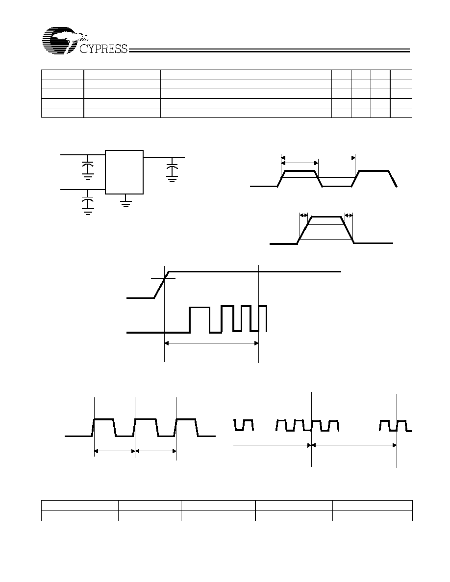
Test Circuit
DC
Output Duty Cycle
Duty Cycle is defined in Figure 1, 50% of V
DD
45
50
55
%
t
3
Rising Edge Slew Rate
Output Clock Rise Time, 20%≠80% of V
DD
/ V
DDL
= 2.5V
0.8
1.4
V/ns
t
4
Falling Edge Slew Rate
Output Clock Fall Time, 80%≠20% of V
DD
/ V
DDL
= 2.5V
0.8
1.4
V/ns
t
5
PLL Lock Time
3
ms
AC Electrical Characteristics (V
DD
= 3.15V≠3.6V) (continued)
Parameter
[3]
Description
Conditions
Min.
Typ. Max.
Unit
0.1
µ
F
AV
DD
0.1
µ
F
V
DD
CLK out
C
LOAD
GND
OUTPUTS
t1
t2
CLK
50%
Figure 1. Duty Cycle Definition; DC = t2/t1
t3
CLK
80%
20%
t4
Figure 2. Rise and Fall Time Definitions
V
DD
80%
Stable @ ±0.1% frequency
t
5
Figure 3. PLL Lock Time
t
9A
t
9B
Figure 4. Cycle-Cycle Jitter
t
10
t
10
...
...
Figure 5. 1000-Cycle Jitter
Ordering Information
Ordering Code
Package Name
Package Type
Operating Range
Operating Voltage
CY24141ZC-3
Z16
16-TSSOP
Commercial
3.3V
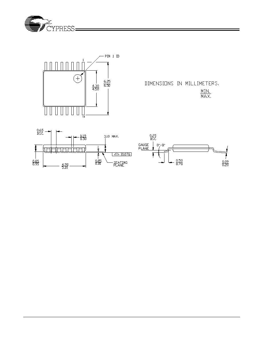
CY24141-3
PRELIMINARY
Document #: 38-07324 Rev. **
Page 5 of 6
© Cypress Semiconductor Corporation, 2002. The information contained herein is subject to change without notice. Cypress Semiconductor Corporation assumes no responsibility for the use
of any circuitry other than circuitry embodied in a Cypress Semiconductor product. Nor does it convey or imply any license under patent or other rights. Cypress Semiconductor does not authorize
its products for use as critical components in life-support systems where a malfunction or failure may reasonably be expected to result in significant injury to the user. The inclusion of Cypress
Semiconductor products in life-support systems application implies that the manufacturer assumes all risk of such use and in doing so indemnifies Cypress Semiconductor against all charges.
MediaClock is a trademark of Cypress Semiconductor. All products and company names mentioned in this document are the
trademarks of their respective holders.
16-lead Thin Shrunk Small Outline Package (4.40-MM Body) Z16
51-85091