 | ÐлекÑÑоннÑй компоненÑ: CY24142 | СкаÑаÑÑ:  PDF PDF  ZIP ZIP |
Äîêóìåíòàöèÿ è îïèñàíèÿ www.docs.chipfind.ru
MediaClockTM
Multimedia Clock Generator
CY24142
Cypress Semiconductor Corporation
·
3901 North First Street
·
San Jose
,
CA 95134
·
408-943-2600
Document #: 38-07532 Rev. *B
Revised January 19, 2005
Features
· Integrated phase-locked loop (PLL)
· Low-jitter, high-accuracy outputs
· 3.3V operation
Benefits
· Integrated high-performance PLL eliminates the need for
-- external loop filter components
· Meets critical timing requirements in complex system
designs
· Enables application compatibility
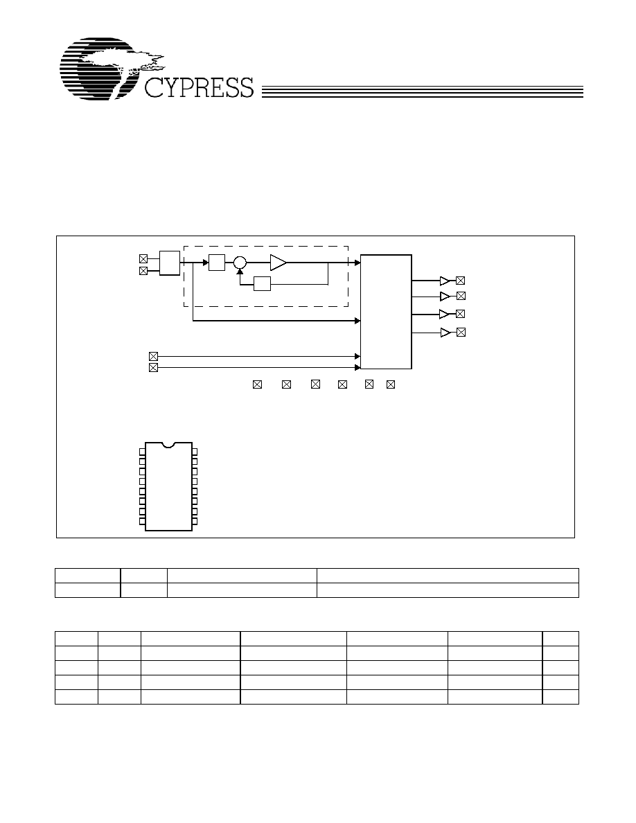
Logic Block Diagram
Pin Configuration
XIN
XOUT
OUTPUT
MULTIPLEXER
AND
DIVIDERS
PLL
OSC.
CLK1 13.5 MHz
Q
P
VCO
VDDL
AVSS
AVDD
VSS
CLK2 54 MHz
CLK3 18.432 MHz
16-pin TSSOP
1
2
3
4
5
6
7
8
9
10
11
12
13
14
15
16
VSS
VSSL
OE2
XIN
XOUT
VDD
AVSS
CLK2
CLK4
CLK3
AVDD
VDDL
NC
CLK1
OE1
CLK4 18.432 MHz
VDD
VSSL
CY24142
OE2
OE1
NC
Frequency Table
Part Number Outputs
Input Frequency
Output Frequency Range
CY24142-01
4
18.432
13.5 MHz, 54 MHz, 2
x
18.432 MHz
Output Enable Options
[1]
OE2
OE1
CLK1 CLK2
CLK3
CLK4
Unit
0
0
13.5
OFF
OFF
OFF
MHz
0
1
13.5
54
18.432
OFF
MHz
1
0
13.5
OFF
OFF
18.432
MHz
1
1
13.5
54
18.432
18.432
MHz
Note:
1. Output driven LOW when "OFF."
CY24142
Document #: 38-07532 Rev. *B
Page 2 of 7
Layout Recommendations
The X
IN
and X
OUT
traces and pads as well as the crystal
should be placed away from any clock traces or noise sources.
Noise coupling into the X
IN
and X
OUT
traces may cause
start-up problems. A pad for a resistor to ground should be laid
out on the X
OUT
trace to be stuffed if necessary, in case
start-up issues occur.
Pin Description
Pin Name
Pin Number
Pin Description
XIN
1
Crystal Input.
V
DD
2
Voltage Supply.
AV
DD
3
Analog Voltage Supply.
OE1
4
Output Enable 1, 0 = CLK 2 and CLK3 off, 1 = CLK 2 and CLK3 on; weak internal
pull-down.
AV
SS
5
Analog Ground.
V
SSL
6
V
DDL
Ground.
NC
7
No Connect; leave floating.
CLK1
8
13.5-MHz Clock Output.
CLK2
9
54-MHz Clock Output; controlled by OE1.
OE2
10
Output Enable 2, 0 = CLK4 off, 1 = CLK4 on; weak internal pull-down.
V
DDL
11
Voltage Supply.
NC 12
No Connect; leave floating.
V
SS
13
Ground.
CLK3
14
18.432-MHz Buffered Reference Output, controlled by OE1.
CLK4
15
18.432-MHz Buffered Reference Output, controlled by OE2.
XOUT
16
Crystal Output.
CY24142
Document #: 38-07532 Rev. *B
Page 3 of 7
Absolute Maximum Conditions
(Above which the useful life may be impaired. For user guide-
lines, not tested.
Supply Voltage (V
DD
, AV
DD
, V
DDL
) ...................0.5 to +7.0V
DC Input Voltage...................................... 0.5V to V
DD
+ 0.5
Storage Temperature (Non-Condensing).... 55
°C to +125°C
Junction Temperature ................................ 40
°C to +125°C
Data Retention @ Tj=125
°C..................................> 10 years
Package Power Dissipation...................................... 350 mW
ESD (Human Body Model) MIL-STD-883.................... 2000V
Recommended Crystal Specifications
Parameter
Description
Comments
Min.
Typ.
Max.
Unit
F
NOM
Nominal crystal frequency
Parallel resonance, fundamental mode, AT cut
18.432
MHz
C
LNOM
Nominal load capacitance
14
pF
R
1
Equivalent series resistance
(ESR)
Fundamental mode
25
R
3
/R
1
Ratio of third overtone mode ESR
to fundamental mode ESR
Ratio used because typical R
1
values are much
less than the maximum spec
3
DL
Crystal drive level
No external series resistor assumed
0.5
2
mW
Recommended Operating Conditions
Parameter
Description
Min.
Typ.
Max.
Unit
V
DD,
AV
DD
, V
DDL
Supply Voltage
3.15
3.45
3.6
V
T
A
Ambient Temperature
0
85
°C
C
LOAD
Max. Load Capacitance
15
pF
T
PU
Power-up time for all V
DD
s to reach minimum specified voltage (power
ramps must be monotonic)
0.05
500
ms
DC Electrical Specifications
Parameter
Description
Conditions
Min.
Typ.
Max.
Unit
I
OH
[2]
Output High Current
V
OH
= V
DD
0.5, V
DD
/V
DDL
= 3.45V
12
24
mA
I
OL
[2]
Output Low Current
V
OL
= 0.5, V
DD
/V
DDL
= 3.45V
12
24
mA
I
IH
Input High Current
V
IH
= V
DD
50
µA
I
IL
Input Low Current
V
IL
= 0V
5
10
µA
V
IH
Input High Voltage
CMOS levels, 70% of V
DD
0.7
V
DD
V
IL
Input Low Voltage
CMOS levels, 30% of V
DD
0.3
V
DD
I
VDD
Supply Current
AV
DD
/V
DD
Current
25
mA
I
VDDL
Supply Current
V
DDL
Current
20
mA
R
DOWN
Pull-down resistor on Inputs
V
DD
= 3.15 to 3.6V, measured V
IN
= 3.45V
100
150
k
C
XTAL
[2]
Crystal Load Capacitance
Total effective load of internal load caps
12.9
pF
Cycle-Cycle Jitter Specifications
(VDD = 3.15V 3.6V)
Parameter
Description
Conditions
1
Typ.
Max.
Unit
t
9
Clock Jitterpeak-peak
Cycle-Cycle Jitter18.432 MHz
20
120
200
ps
t
9
Clock Jitterpeak-peak
Cycle-Cycle Jitter54 MHz
40
150
250
ps
t
9
Clock Jitterpeak-peak
Cycle-Cycle Jitter13.5 MHz
20
120
200
ps
Note:
2. Guaranteed by characterization, not 100% tested.
CY24142
Document #: 38-07532 Rev. *B
Page 4 of 7
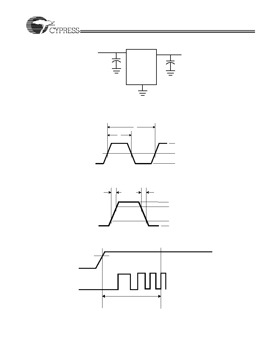
Test and Measurement Set-up
Voltage and Timing Definitions
0.1
µF
V
DDs
Outputs
C
LOAD
GND
DUT
Figure 1. Duty Cycle Definition
Figure 2. ER = (0.6 x V
DD
) /t3, EF = (0.6 x V
DD
) /t4
Clock
Output
V
DD
50% of V
DD
0V
t
1
t
2
Clock
Output
t
3
t
4
V
DD
80% of V
DD
20% of V
DD
0V
V
DD
/V
DDL
/AV
DD
3.15V
Output stable within PPM Spec.
t
5
Figure 3. PLL Lock Time
CY24142
Document #: 38-07532 Rev. *B
Page 5 of 7
Ordering Information
Ordering Code
Package Type
Operating Range
Operating Voltage
Standard
CY24142ZC-01
16-pin TSSOP
Commercial
3.45V
CY24142ZC-01T
16-pin TSSOP Tape and Reel
Commercial
3.45V
Lead-free
CY24142ZXC-01
16-pin TSSOP
Commercial
3.45V
CY24142ZXC-01T
16-pin TSSOP Tape and Reel
Commercial
3.45V
t
cycle,i
t
cycle,i+1
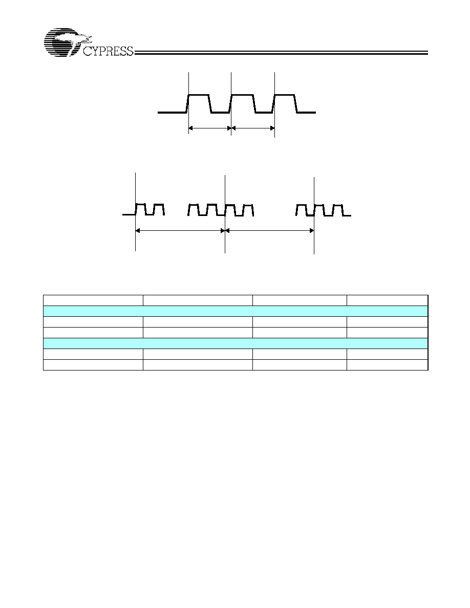
Figure 4. 54MOUT, LCLK Cycle-to-Cycle Jitter
t
6
= t
cycle,i
- t
cycle,i+1
t
1000cycle,i
t
1000cycle,i+1
...
...
Figure 5. 54MOUT, LCLK 1000 Cycle Jitter
t
7
= t
1000cycle,i
- t
1000cycle,i+1
1000 cycles
1000 cycles