 | –≠–ª–µ–∫—Ç—Ä–æ–Ω–Ω—ã–π –∫–æ–º–ø–æ–Ω–µ–Ω—Ç: CY24154 | –°–∫–∞—á–∞—Ç—å:  PDF PDF  ZIP ZIP |
PRELIMINARY
MediaClockTM
54-MHz MPEG Clock Generator with Digital VCXO
CY24154
Cypress Semiconductor Corporation
∑
3901 North First Street
∑
San Jose
∑
CA 95134
∑
408-943-2600
Document #: 38-07321 Rev. *A
Revised December 14, 2002
Features
Benefits
∑ Integrated phase-locked loop (PLL)
Highest-performance PLL tailored to multimedia applications
∑ Low-jitter, high-accuracy outputs
Meets critical timing requirements in complex system designs
∑ VCXO with digital adjust
Large ±150 ppm range, better linearity
∑ 3.3V Operation
Enables application compatibility
∑ Serial Programming Interface (SPI)
Enables dynamic VCXO configuration
Part Number
Outputs
Input Frequency Range
Output Frequencies
CY24154
1
13.5-MHz Pullable Crystal per
Cypress Specification
1 copy of 54 MHz (3.3V)
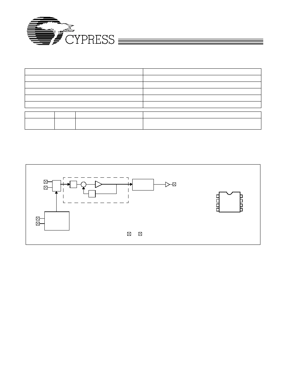
Logic Block Diagram
13.5 XIN
XOUT
54 MHz
OUTPUT
DIVIDER
PLL
OSC
Q
P
VCO
VDD
VSS
Serial
Programming
Interface
SCLK
SDAT
Pin Configurations
8-pin SOIC
CY24154
1
2
3
4
XOUT
XIN
SDAT
54 MHz
VSS
N/C
SCLK
5
6
7
8
VDD
PRELIMINARY
CY24154
Document #: 38-07321 Rev. *A
Page 2 of 6
Pullable Crystal Specifications
Absolute Maximum Conditions
Recommended Operating Conditions
Summary
Name
Pin Number
Description
X
IN
1
Reference Crystal Input
V
DD
2
Output Voltage Supply
SDAT
3
Serial Data Input
V
SS
4
Output Ground
S
CLK
5
Serial Clock Input
54 MHz
6
54-MHz Clock Output
N/C
7
No Connect
X
OUT
[1]
8
Reference Crystal Output
Parameter
Name
Min.
Typ.
Max.
Unit
CR
load
Crystal Load Capacitance
14
pF
C0/C1
240
ESR
Equivalent Series Resistance
35
50
T
o
Operating Temperature
0
70
∞C
Crystal Accuracy
Crystal Accuracy
+20
ppm
TT
s
Stability over temperature and aging
+50
ppm
Parameter
Description
Min.
Max.
Unit
V
DD
Supply Voltage
≠0.5
7.0
V
T
S
Storage Temperature
[2]
≠65
125
∞C
T
J
Junction Temperature
125
∞C
Digital Inputs
V
SS
≠ 0.3
V
DD
+ 0.3
V
Digital Outputs Referred to V
DD
V
SS
≠ 0.3
V
DD
+ 0.3
V
Electrostatic Discharge
2
kV
Parameter
Description
Min.
Typ.
Max.
Unit
V
DD
Operating Voltage
3.135
3.3
3.465
V
T
A
Ambient Temperature
0
70
∞ C
C
LOAD
Max Load Capacitance
15
pF
f
REF
Reference Frequency
13.5
MHz
t
PU
Power-up time for all VDD's to
reach minimum specified voltage
(power ramps must be
monotonic)
0.05
500
ms
Note:
1.
Float X
OUT
if X
IN
is externally driven.
2.
Rated for 10 years.
PRELIMINARY
CY24154
Document #: 38-07321 Rev. *A
Page 3 of 6
DC Electrical Characteristics
AC Electrical
Characteristics
(V
DD
= 3.3V)
Serial Programming Interface for the 24154
Introduction
The CY24154 has a 2-wire serial interface that can be used
for digital VCXO control. SCLK is the Serial Clock input line,
and SDAT is the Serial Data input line.
The SPI address for the 24154 is:
VCXO control is at address 13h [00010011], bits [7.0]. The
MSB, bit 7, is shifted in first.
The VCXO register data can be any value between 00H≠FFH.
As you increase the value, the capacitance on the Xin and the
Xout pins will increase, thereby decreasing the xtal frequency.
Note:
3.
Not 100% tested.
Parameter
Name
Description
Min.
Typ.
Max.
Unit
I
OH
Output HIGH Current
V
OH
= V
DD
≠ 0.5, V
DD
= 3.3 V
12
24
mA
I
OL
Output LOW Current
V
OL
= 0.5, V
DD
=3.3 V
12
24
mA
C
IN
Input Capacitance
7
pF
I
IZ
Input Leakage Current
5
µ
A
f
xo
VCXO Pullability Range
≠150
+150
ppm
I
DD
Supply Current
Sum of Core and Output Current
30
mA
Parameter
[3]
Name
Description
Min.
Typ.
Max.
Unit
DC
Output Duty Cycle
Duty Cycle is Defined in Figure 1, 50% of V
DD
45
50
55
%
t
3
Rising Edge Slew Rate
Output Clock Rise Time, 20%≠80% of V
DD
0.8
1.4
V/ns
t
4
Falling Edge Slew Rate
Output Clock Fall Time, 80%≠20% of V
DD
0.8
1.4
V/ns
t
9
Clock Jitter
Peak to Peak Period Jitter
100
ps
t
10
PLL Lock Time
3
ms
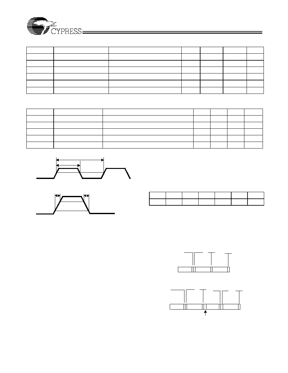
Figure 1. Duty Cycle Definition; DC = t2/t1
54 MHz
t1
t2
50%
Figure 2. Rise and Fall Time Definitions
54 MHz
t3
t4
80%
20%
A6
A5
A4
A3
A2
A1
A0
1
1
0
1
0
0
1
SDAT Write
Start Signal
Device
Address
7-bit
R/W = 0
1-bit
8-bit
Register
Address
Slave
1-bit
ACK
Slave
1-bit
ACK
8-bit
Register
Data
Stop Signal
Slave
1-bit
ACK
SDAT Read
Start Signal
Device
Address
7 Bit
R/W = 0
1 Bit
8 Bit
Register
Address
Slave
1 Bit
ACK
Slave
1 Bit
ACK
7 Bit
Device
Address
Stop Signal
8 Bit
Register
Data
Master
1 Bit
ACK
R/W = 1
1 Bit
ACK
Slave
1 Bit
Start Signal
Repeated
Figure 3. Data Frame Architecture
PRELIMINARY
CY24154
Document #: 38-07321 Rev. *A
Page 4 of 6
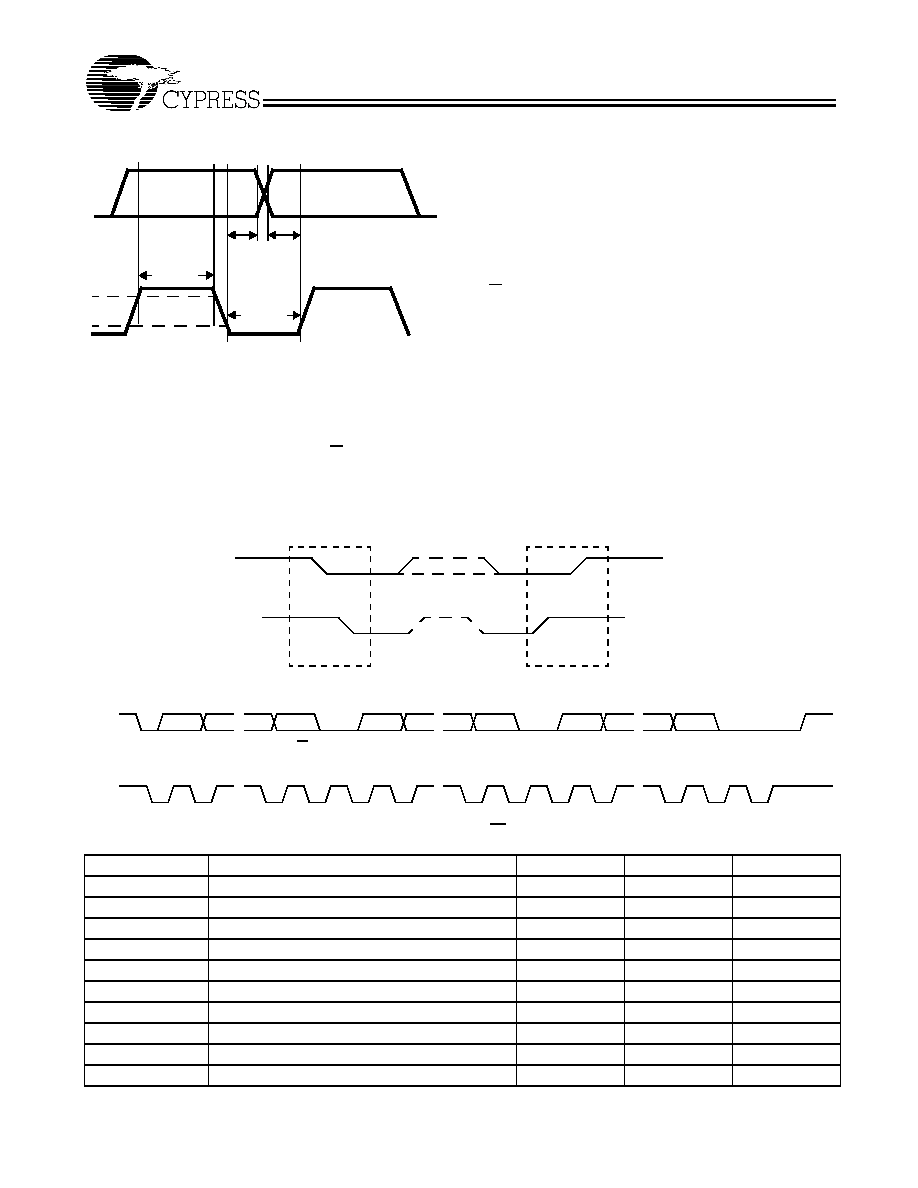
Programmable Interface Timing
The CY24154 utilizes a 2-serial-wire interface SDAT and
SCLK that operates up to 400 kbits/sec in Read or Write mode.
The basic Write serial format is as follows:
Start bit; 7-bit Device Address (DA); R/W Bit; Slave Clock
Acknowledge (ACK); 8-bit Memory Address (MA); ACK; 8-bit
Data; ACK; 8-bit Data in MA+1 if desired; ACK; 8-bit Data in
MA+2; ACK; etc. until STOP bit.The basic serial format is illus-
trated in Figure 3.
Data Valid
Data is valid when the clock is HIGH, and may only be transi-
tioned when the clock is LOW, as illustrated in Figure 4.
Data Frame
Every new data frame is indicated by a start and stop
sequence, as illustrated in Figure 5.
Start Sequence ≠ Start Frame is indicated by SDAT going
LOW when SCLK is HIGH. Every time a start signal is given,
the next 8-bit data must be the device address (7 bits) and a
R/W bit.
Stop Sequence ≠ Stop Frame is indicated by SDAT going
HIGH when SCLK is HIGH. A Stop Frame frees the bus for
writing to another part on the same bus or writing to another
random register address.
Acknowledge Pulse
During Write mode the CY24154 will respond with an
Acknowledge pulse after every 8 bits. This is accomplished by
pulling the SDAT line LOW during the N*9
th
clock cycle as
illustrated in Figure 6. (N = the number of 8 bit segments trans-
mitted.) During Read Mode the acknowledge pulse after the
data packet is sent is generated by the master.
SDAT
SCLK
Data Valid
Transition
to next Bit
CLKLOW
CLKHIGH
VIH
VIL
tSU
tDH
Figure 4. Data Valid and Data Transition Periods
Parameter
Description
Min.
Max.
Unit
f
SCLK
Frequency of SCLK
400
kHz
Start Mode Time from SDA LOW to SCL LOW
0.6
µ
s
CLK
LOW
SCLK LOW Period
1.3
µ
s
CLK
HIGH
SCLK HIGH Period
0.6
ns
t
SU
Data Transition to SCLK HIGH
100
ns
t
DH
Data Hold (SCLK LOW to Data Transition)
0
ns
Rise Time of SCLK and SDAT
300
ns
Fall Time of SCLK and SDAT
300
ns
Stop Mode Time from SCLK HIGH to SDAT HIGH
0.6
µ
s
Stop Mode to Start Mode
1.3
µ
s
SDAT
SCLK
START
Transition
to next Bit
STOP
Figure 5. Start and Stop Frame
SDAT
SCLK
DA6
DA5 DA0
R/W
ACK
RA7
RA6 RA1
RA0
ACK
STOP
START
ACK
D7
D6
D1
D0
+
+
+
+
+
+
Figure 6. Frame Format (Device Address, R/W, Register Address, Register Data
PRELIMINARY
CY24154
Document #: 38-07321 Rev. *A
Page 5 of 6
© Cypress Semiconductor Corporation, 2002. The information contained herein is subject to change without notice. Cypress Semiconductor Corporation assumes no responsibility for the use
of any circuitry other than circuitry embodied in a Cypress Semiconductor product. Nor does it convey or imply any license under patent or other rights. Cypress Semiconductor does not authorize
its products for use as critical components in life-support systems where a malfunction or failure may reasonably be expected to result in significant injury to the user. The inclusion of Cypress
Semiconductor products in life-support systems application implies that the manufacturer assumes all risk of such use and in doing so indemnifies Cypress Semiconductor against all charges.
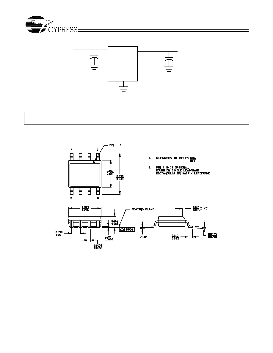
Test Circuit
Ordering Information
Package Diagram
All product and company names mentioned in this document may be the trademarks of their respective holders.
0.1
µ
F
V
DD
CLK
OUT
C
LOAD
GND
OUTPUTS
Ordering Code
Package Name
Package Type
Operating Range
Operating Voltage
CY24154SC
S8
8-pin SOIC
Commercial
3.3V
8-lead (150-mil) SOIC S8
51-85066-A