 | –≠–ª–µ–∫—Ç—Ä–æ–Ω–Ω—ã–π –∫–æ–º–ø–æ–Ω–µ–Ω—Ç: CY24204-2 | –°–∫–∞—á–∞—Ç—å:  PDF PDF  ZIP ZIP |
MediaClockTM
DTV, STB Clock Generator
CY24204
Cypress Semiconductor Corporation
∑
3901 North First Street
∑
San Jose
,
CA 95134
∑
408-943-2600
Document #: 38-07450 Rev. **
Revised April 9, 2003
Features
Benefits
∑ Integrated phase-locked loop (PLL)
Internal PLL with up to 400-MHz internal operation
∑ Low jitter, high-accuracy outputs
Meets critical timing requirements in complex system designs
∑ VCXO with Analog Adjust
Large ±150-ppm range, better linearity
∑ 3.3V operation
Enables application compatibility
Part Number
Outputs
Input Frequency
Output Frequency Range
CY24204-1
3
27MHz Crystal Input
One copy of 27-MHz reference clock output, two copies of
27/27.027/74.250/74.175 MHz (frequency selectable)
CY24204-2
4
27MHz Crystal Input
Two copies of 27-MHz reference clock output, two copies of
27/27.027/74.250/74.175 MHz (frequency selectable)
CY24204-3
4
27MHz Crystal Input
Two copies of 27-MHz reference clock output, two copies of
27/27.027/74.250/74.17582418 MHz (frequency selectable)
Frequency Select Options
OE
FS1
FS0
CLK1/CLK2 (-1,-2)
[1]
CLK1/CLK2 (-3)
[1]
REFCLK 1/2
Unit
0
0
0
off
off
27
MHz
0
0
1
off
off
27
MHz
0
1
0
off
off
27
MHz
0
1
1
off
off
27
MHz
1
0
0
27
27
27
MHz
1
0
1
27.027
27.027
27
MHz
1
1
0
74.250
74.250
27
MHz
1
1
1
74.175
74.17582418
27
MHz
Note:
1.
"off" = output is driven high
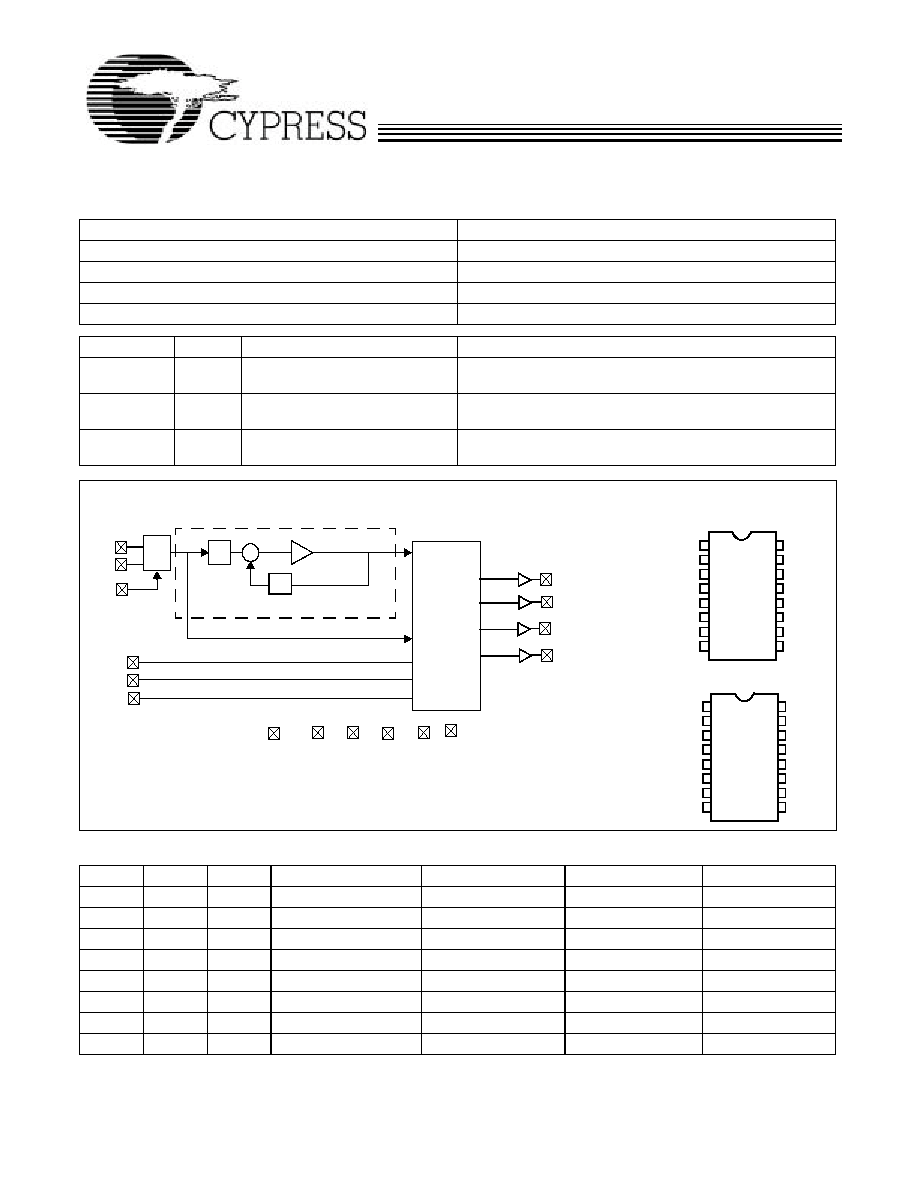
Block Diagram
XIN
XOUT
OUTPUT
MULTIPLEXER
AND
DIVIDERS
PLL
OSC.
CLK1
Q
P
VCO
VDDL
AVSS
AVDD
VSS
FS0
FS1
CLK2
REFCLK1
VSSL
VDD
16-pin TSSOP
1
2
3
4
5
6
7
8
9
10
11
12
13
14
15
16
VSS
VSSL
FS0
XIN
XOUT
VDD
VCXO
AVSS
REFCLK1
OE
FS1
AVDD
VDDL
Pin Configurations
NC
CLK2
OE
VCXO
CLK1
16-pin TSSOP
1
2
3
4
5
6
7
8
9
10
11
12
13
14
15
16
VSS
VSSL
FS0
XIN
XOUT
VDD
VCXO
AVSS
REFCLK1
OE
FS1
AVDD
VDDL
CLK2
CLK1
REFCLK2
24
20
4-
2
,
3
242
04
-
1
REFCLK2 (-2, -3)
CY24204
Document #: 38-07450 Rev. **
Page 2 of 6
Pin Description
Name
Pin Number
Description
XIN
1
Reference Crystal Input
V
DD
2
Voltage Supply
AV
DD
3
Analog Voltage Supply
VCXO
4
Input analog control for VCXO
AV
SS
5
Analog Ground
V
SSL
6
CLK Ground
N/C (-1)
7
No Connect
REFCLK2 (-2)
7
Reference Clock output
REFCLK1
8
Reference Clock output
CLK1 (-1, -2)
9
27-/27.027-/74.250-/74.175-MHz clock output (frequency selectable)
CLK1 (-3)
9
27-/27.027-/74.250-/74.17582418-MHz clock output (frequency selectable)
FS0
10
Frequency Select 0, weak internal pull-up
V
DDL
11
CLK Voltage Supply
CLK2 (-1, -2)
12
27-/27.027-/74.250-/74.175-MHz clock output (frequency selectable)
CLK2 (-3)
12
27-/27.027-/74.250-/74.17582418-MHz clock output (frequency selectable)
V
SS
13
Ground
FS1
14
Frequency Select 1, weak internal pull-up
OE
15
Output Enable, weak internal pull-up
XOUT
16
Reference Crystal Output
CY24204
Document #: 38-07450 Rev. **
Page 3 of 6
Absolute Maximum Conditions
Supply Voltage (V
DD
, AV
DDL
, V
DDL
)..................≠0.5 to +7.0V
DC Input Voltage ...................................... ≠0.5V to V
DD
+ 0.5
Storage Temperature (Non-Condensing) .... ≠55
∞
C to +125
∞
C
Junction Temperature ................................ ≠40
∞
C to +125
∞
C
Data Retention @ Tj=125
∞
C..................................> 10 years
Package Power Dissipation...................................... 350 mW
ESD (Human Body Model) MIL-STD-883.................... 2000V
(Above which the useful life may be impaired. For user guide-
lines, not tested.)
DC Electrical Specifications
Pullable Crystal Specifications
Parameter
Description
Comments
Min.
Typ.
Max.
Units
F
NOM
Nominal crystal frequency
Parallel resonance, funda-
mental mode, AT cut
27.0
MHz
C
LNOM
Nominal load capacitance
14
pF
R
1
Equivalent series resis-
tance (ESR)
Fundamental mode
25
R
3
/R
1
Ratio of third overtone
mode ESR to fundamental
mode ESR
Ratio used because typical
R
1
values are much less than
the maximum spec
3
DL
Crystal drive level
No external series resistor
assumed
0.5
2
mW
F
3SEPHI
Third overtone separation
from 3*F
NOM
High side
300
ppm
F
3SEPLO
Third overtone separation
from 3*F
NOM
Low side
≠150
ppm
C
0
Crystal shunt capacitance
7
pF
C
0
/C
1
Ratio of shunt to motional
capacitance
180
250
C
1
Crystal motional capaci-
tance
14.4
18
21.6
fF
Recommended Operating Conditions
Parameter
Description
Min.
Typ.
Max.
Unit
V
DD
/AV
DDL
/V
DDL
Operating Voltage
3.135
3.3
3.465
V
T
A
Ambient Temperature
0
70
∞C
C
LOAD
Max. Load Capacitance
15
pF
t
PU
Power-up time for all V
DD
`s to reach minimum specified
voltage (power ramps must be monotonic)
0.05
500
ms
Parameter
[2]
Name
Description
Min.
Typ.
Max.
Unit
I
OH
Output High Current
V
OH
= V
DD
≠ 0.5, V
DD
/V
DDL
= 3.3V
12
24
mA
I
OL
Output Low Current
V
OL
= 0.5, V
DD
/V
DDL
= 3.3V
12
24
mA
V
IH
Input High Voltage
CMOS levels, 70% of V
DD
0.7
V
DD
V
IL
Input Low Voltage
CMOS levels, 30% of V
DD
0.3
V
DD
I
VDD
Supply Current
AV
DD
/V
DD
Current
25
mA
I
VDDL
Supply Current
V
DDL
Current (V
DDL
= 3.47V)
20
mA
C
IN
Input Capacitance
7
pF
f
XO
V
CXO
pullability range
±150
ppm
V
VCXO
V
CXO
input range
0
V
DD
V
R
UP
Pull-up resistor on inputs V
DD
= 3.14 to 3.47V, measured at V
IN
= 0V
100
150
k
Note:
2.
Not 100% tested.
CY24204
Document #: 38-07450 Rev. **
Page 4 of 6
AC Electrical Specifications
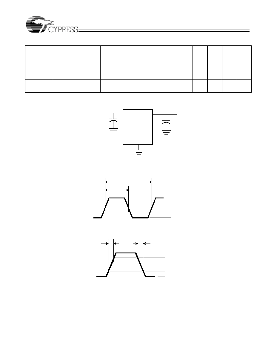
Test and Measurement Set-up
Voltage and Timing Definitions
Parameter
2
Name
Description
Min.
Typ.
Max.
Unit
DC
Output Duty Cycle
Duty Cycle is defined in Figure 1; t1/t2, 50% of V
DD
45
50
55
%
ER
Rising Edge Rate
Output Clock Edge Rate, Measured from 20% to
80% of V
DD
, C
LOAD
= 15 pF See Figure 2.
0.8
1.4
V/ns
EF
Falling Edge Rate
Output Clock Edge Rate, Measured from 80% to
20% of V
DD
, C
LOAD
= 15 pF See Figure 2.
0.8
1.4
V/ns
t
9
Clock Jitter
CLK1, CLK2 Peak-Peak period jitter
120
ps
t
10
PLL Lock Time
3
ms
0.1
µ
F
V
DDs
Outputs
C
LOAD
GND
DUT
Clock
Output
V
DD
50% of V
DD
0V
t
1
t
2
Figure 1. Duty Cycle Definition
Clock
Output
t
3
t
4
V
DD
80% of V
DD
20% of V
DD
0V
Figure 2. ER = (0.6 x V
DD
) /t3, EF = (0.6 x V
DD
) /t4
CY24204
Document #: 38-07450 Rev. **
Page 5 of 6
© Cypress Semiconductor Corporation, 2003. The information contained herein is subject to change without notice. Cypress Semiconductor Corporation assumes no responsibility for the use
of any circuitry other than circuitry embodied in a Cypress Semiconductor product. Nor does it convey or imply any license under patent or other rights. Cypress Semiconductor does not authorize
its products for use as critical components in life-support systems where a malfunction or failure may reasonably be expected to result in significant injury to the user. The inclusion of Cypress
Semiconductor products in life-support systems application implies that the manufacturer assumes all risk of such use and in doing so indemnifies Cypress Semiconductor against all charges.
Ordering Information
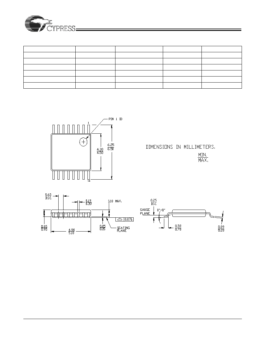
Package Drawing and Dimensions
MediaClock is a trademark of Cypress Semiconductor Corporation. All product and company names mentioned in this document
may be the trademarks of their respective holders.
Ordering Code
Package Name
Package Type
Operating Range
Operating Voltage
CY24204ZC-1
Z16
16-Pin TSSOP
Commercial
3.3V
CY24204ZC-1T
Z16
16-Pin TSSOP
Commercial
3.3V
CY24204ZC-2
Z16
16-Pin TSSOP
Commercial
3.3V
CY24204ZC-2T
Z16
16-Pin TSSOP
Commercial
3.3V
CY24204ZC-3
Z16
16-Pin TSSOP
Commercial
3.3V
CY24204ZC-3T
Z16
16-Pin TSSOP
Commercial
3.3V
16-Lead Thin Shrunk Small Outline Package (4.40 MM Body) Z16
51-85091-**

CY24204
Document #: 38-07450 Rev. **
Page 6 of 6
Document History Page
Document Title: CY24204 MediaClockTM DTV, STB Clock Generator
Document Number: 38-07450
REV.
ECN NO.
Issue
Date
Orig. of
Change
Description of Change
**
123842
04/10/03
CKN
New Data Sheet