 | –≠–ª–µ–∫—Ç—Ä–æ–Ω–Ω—ã–π –∫–æ–º–ø–æ–Ω–µ–Ω—Ç: CY24712 | –°–∫–∞—á–∞—Ç—å:  PDF PDF  ZIP ZIP |
MediaClockTM
Set-top Box Clock Generator with VCXO
CY24712
Cypress Semiconductor Corporation
∑
3901 North First Street
∑
San Jose
∑
CA 95134
∑
408-943-2600
Document #: 38-07319 Rev. *B
Revised December 14, 2002
Features
Benefits
∑ Integrated phase-locked loop (PLL)
High-performance PLL tailored for Set Top Box applications
∑ Low-jitter, high-accuracy outputs
Meets critical timing requirements in complex system designs
∑ VCXO with analog adjust
Large ±150-ppm range, better linearity
∑ 3.3V Operation
Meet industry standard voltage platforms
∑ 8-pin SOIC
Industry standard packaging saves on board space
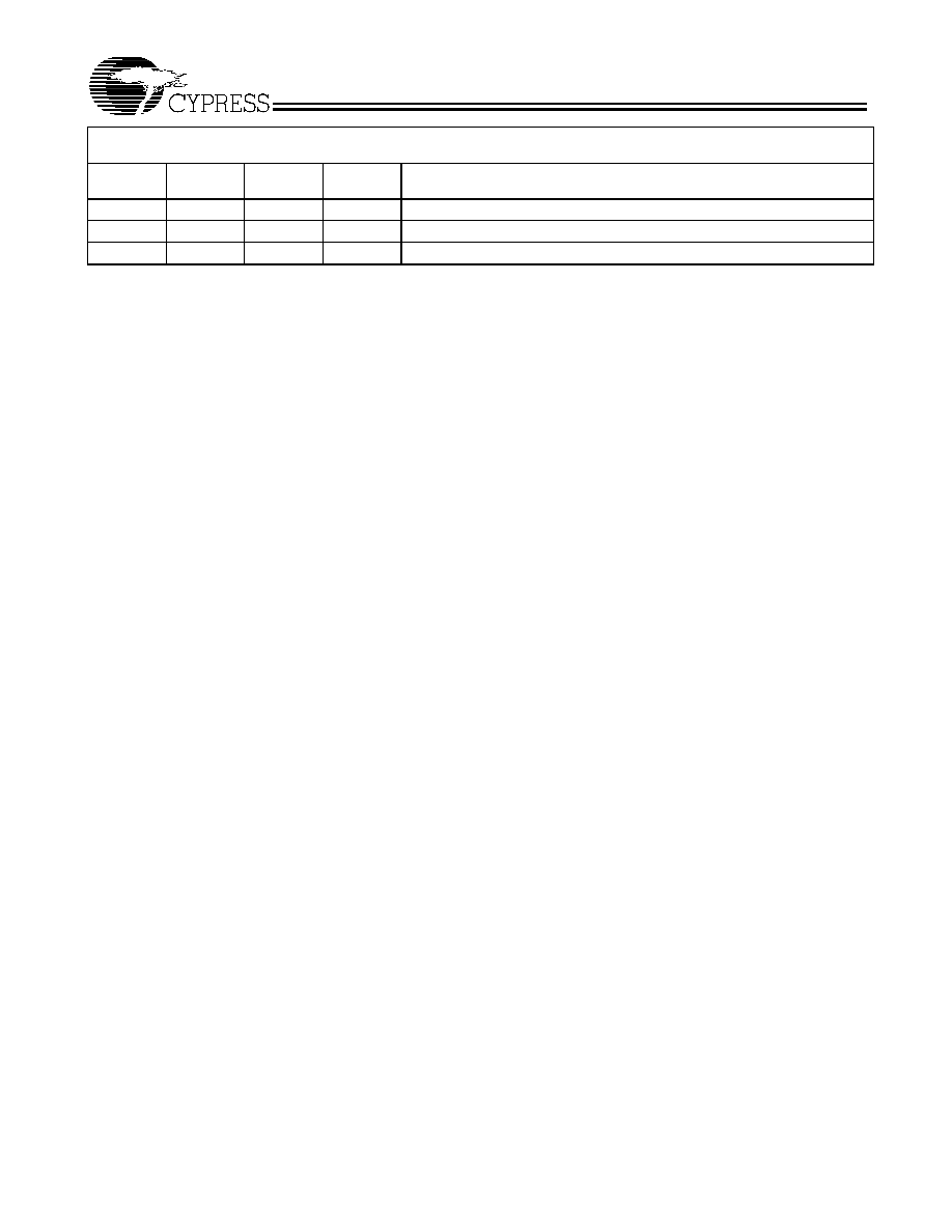
Part Number
Outputs
Input Frequency Range
Output Frequencies
CY24712
3
27-MHz pullable crystal input
per Cypress specification
11.0592 MHz, 13.5 MHz, 27 MHz
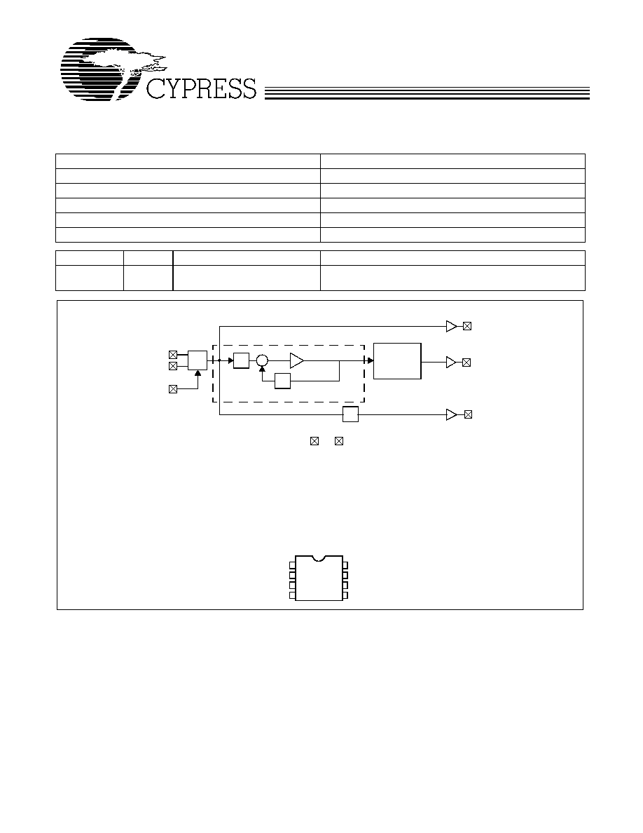
Logic Block Diagram
27 XIN
XOUT
CLK_A 11.0592 MHz
OUTPUT
DIVIDERS
PLL
OSC
VCXO
CLK_C 27 MHz
Q
/2
VCO
VDD
VSS
CLK_B 13.5 MHz
P
8-pin SOIC
CY24712
Pin Configuration
1
2
3
4
XOUT
XIN
VCXO
CLK_B
VSS
CLK_C
CLK_A
5
6
7
8
VDD
CY24712
Document #: 38-07319 Rev. *B
Page 2 of 5
Summary
Pin Name
Pin Number
Pin Description
XIN
1
Reference Crystal Input
VDD
2
3.3V Voltage Supply
VCXO
3
Input Analog Control for VCXO
VSS
4
Ground
CLK_B
5
13.5-MHz Clock Output
CLK_A
6
11.0592-MHz Clock Output
CLK_C
7
27-MHz Clock Output
XOUT
[1]
8
Reference Crystal Output
Pullable Crystal Specifications
Parameter
Description
Min.
Typ.
Max.
Unit
CRYSTAL
Load
Load Capacitance
14
pF
C0/C1
240
ESR
35
T
o
Operating Temperature
0
70
∞C
Acc
init
Initial Accuracy
±30
ppm
Stability
Temperature plus Aging Stability
±80
ppm
Absolute Maximum Conditions
Parameter
Description
Min.
Max.
Unit
V
DD
Supply Voltage
≠0.5
7.0
V
T
S
Storage Temperature
[2]
≠65
125
∞C
T
J
Junction Temperature
125
∞C
Digital Inputs
V
SS
≠ 0.3
V
DD
+ 0.3
V
Digital Outputs referred to V
DD
V
SS
≠ 0.3
V
DD
+ 0.3
V
Electrostatic Discharge
2000
V
Analog Input
≠0.5
7.0
V
Recommended Operating Conditions
Parameter
Description
Min.
Typ.
Max.
Unit
V
DD
Operating Voltage
3.135
3.3
3.465
V
T
A
Ambient Temperature
0
70
∞C
C
LOAD
Max. Load Capacitance
15
pF
f
REF
Reference Frequency
27
MHz
t
PU
Power-up time for all VDD's to
reach minimum specified voltage
(power ramps must be monotonic)
0.05
500
ms
DC Electrical Characteristics
Parameter
Description
Conditions
Min.
Typ.
Max.
Unit
I
OH
Output High Current
V
OH
= V
DD
≠ 0.5, V
DD
= 3.3V
12
24
mA
I
OL
Output Low Current
V
OL
= 0.5, V
DD
= 3.3V
12
24
mA
C
IN
Input Capacitance
7
pF
I
IZ
Input Leakage Current
5
µ
A
f
XO
VCXO pullability range
[3]
±150
ppm
V
VCXO
VCXO input range
0
V
DD
V
I
VDD
Supply Current
36
mA
CY24712
Document #: 38-07319 Rev. *B
Page 3 of 5
Notes:
1.
Float XOUT if XIN is externally driven.
2.
Rated for 10 years.
3.
Must meet pullable crystal specifications.
DC Electrical Characteristics
Parameter
Description
Conditions
Min.
Typ.
Max.
Unit
AC Electrical Characteristics (VDD = 3.3V)
Parameter
[4]
Description
Conditions
Min.
Typ.
Max.
Unit
DC
Output Duty Cycle
Duty Cycle is defined in Figure 1 50% of V
DD
45
50
55
%
ER
0
Rising Edge Rate
Output Clock Edge Rate, Measured from 20%
to 80% of
V
DD,
C
LOAD
= 15 pF Figure 2.
0.8
1.4
V/ns
EF
1
Falling Edge Rate
Output Clock Edge Rate, Measured from 80%
to 20% of
V
DD,
C
LOAD
= 15 pF Figure 2.
0.8
1.4
V/ns
t
9
Clock Jitter
Peak-Peak period jitter
300
350
ps
t
10
PLL Lock Time
3
ms
Note:
4.
Not 100% tested.
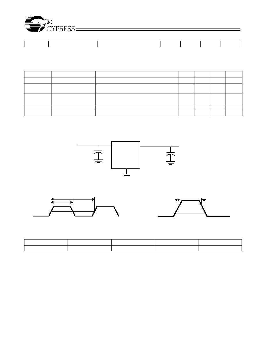
Test Circuit
0.1
µ
F
VDD
CLK out
C LOAD
GND
OUTPUTS
t1
t2
CLK
50%
50%
Figure 1. Duty Cycle Definition; DC = t2/t1
t3
CLK
80%
20%
t4
igure 2. Rise and Fall Time Definitions: ER = 0.6 x V
DD
/t3,
EF = 0.6 x V
DD
/t4
Ordering Information
Ordering Code
Package Name
Package Type
Operating Range
Operating Voltage
CY24712SC
S8
8-pin SOIC
Commercial
3.3V
CY24712
Document #: 38-07319 Rev. *B
Page 4 of 5
© Cypress Semiconductor Corporation, 2002. The information contained herein is subject to change without notice. Cypress Semiconductor Corporation assumes no responsibility for the use
of any circuitry other than circuitry embodied in a Cypress Semiconductor product. Nor does it convey or imply any license under patent or other rights. Cypress Semiconductor does not authorize
its products for use as critical components in life-support systems where a malfunction or failure may reasonably be expected to result in significant injury to the user. The inclusion of Cypress
Semiconductor products in life-support systems application implies that the manufacturer assumes all risk of such use and in doing so indemnifies Cypress Semiconductor against all charges.
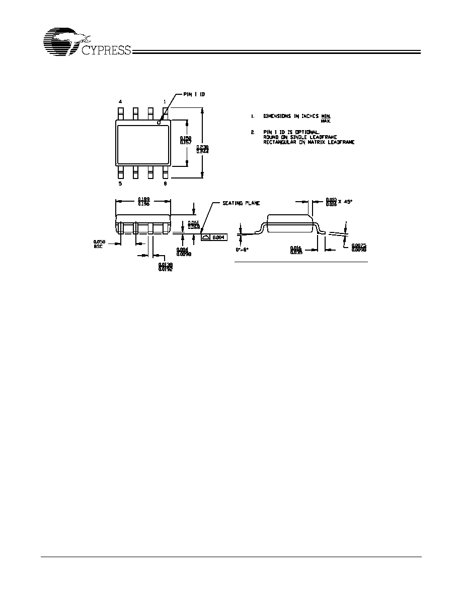
Package Diagram
All product and company names mentioned in this document are the trademarks of their respective holders.
8-pin (150-mil) SOIC S8
51-85066-A
CY24712
Document #: 38-07319 Rev. *B
Page 5 of 5
Document Title: CY24712 MediaClockTM Set-top Box Clock Generator with VCXO
Document Number: 38-07319
REV.
ECN No.
Issue
Date
Orig. of
Change
Description of Change
**
111555
02/29/02
CKN
New Data Sheet
*A
113937
05/02/02
CKN
Removed Kony from the Pullable Crystal Specification table, p. 2
*B
121887
12/14/02
RBI
Power up requirements added to Operating Conditions Information