Äîêóìåíòàöèÿ è îïèñàíèÿ www.docs.chipfind.ru
Field- and Factory-Programmable Spread Spectrum
Clock Generator for EMI Reduction
CY25100
Cypress Semiconductor Corporation
·
3901 North First Street
·
San Jose
,
CA 95134
·
408-943-2600
Document #: 38-07499 Rev. *D
Revised March 24, 2004
Features
· Wide operating output (SSCLK) frequency range
-- 3200 MHz
· Programmable spread spectrum with nominal 31.5-kHz
modulation frequency
-- Center spread: ±0.25% to ±2.5%
-- Down spread: 0.5% to 5.0%
· Input frequency range
-- External crystal: 830 MHz fundamental crystals
-- External reference: 8166 MHz Clock
· Integrated phase-locked loop (PLL)
· Field-programmable
-- CY25100SCF and CY25100SIF, 8-pin SOIC
-- CY25100ZCF and CY25100ZIF, 8-pin TSSOP
· Programmable crystal load capacitor tuning array
· Low cycle-to-cycle jitter
· 3.3V operation
· Commercial and Industrial operation
· Spread Spectrum On/Off function
· Power-down or Output Enable function
Benefits
· Services most PC peripherals, networking, and consumer
applications.
· Provides wide range of spread percentages for maximum
electromagnetic interference (EMI) reduction, to meet
regulatory agency electromagnetic compliance (EMC)
requirements. Reduces development and manufacturing
costs and time-to-market.
· Eliminates the need for expensive and difficult to use
higher-order crystals.
· Internal PLL to generate up to 200-MHz output. Able to
generate custom frequencies from an external crystal or a
driven source.
· In-house programming of samples and prototype quantities
is available using the CY3672 programming kit and
CY3690 (TSSOP) or CY3691 (SOIC) socket adapter.
Production quantities are available through Cypress's
value-added distribution partners or by using third-party
programmers from BP Microsystems, HiLo Systems, and
others.
· Enables fine-tuning of output clock frequency by adjusting
C
Load
of the crystal. Eliminates the need for external C
Load
capacitors.
· Suitable for most PC, consumer, and networking applica-
tions
· Application compatibility in standard and low-power
systems
· Provides ability to enable or disable spread spectrum with
an external pin.
· Enables low-power state or output clocks to High-Z state.
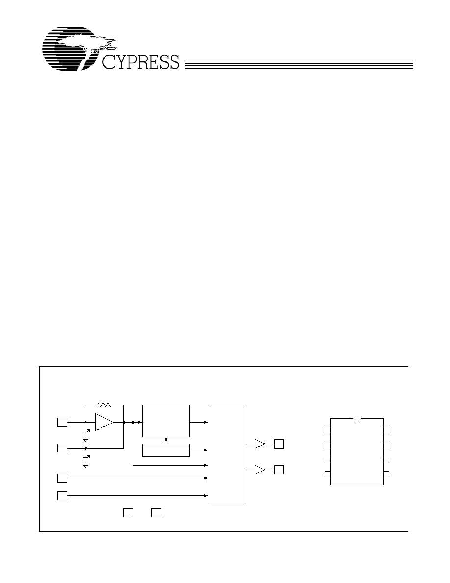
Logic Block Diagram
PLL
with
MODULATION
CONTROL
PROGRAMMABLE
CONFIGURATION
OUTPUT
DIVIDERS
and
MUX
3
2
4
8
1
5
7
6
VDD
VSS
REFCLK
SSCLK
XOUT
XIN
PD# or OE
SSON#
RFB
C
XOUT
C
XIN
4
8
VDD
6
7
VSS
REFCLK
SSON#
1
2
3
XOUT
XIN/CLKIN
PD#/OE
SSCLK
5
Pin Configuration
CY25100
8-pin SOIC/TSSOP
CY25100
Document #: 38-07499 Rev. *D
Page 2 of 11
General Description
The CY25100 is a Spread Spectrum Clock Generator (SSCG)
IC used for the purpose of reducing EMI found in today's
high-speed digital electronic systems.
The device uses a Cypress proprietary PLL and Spread
Spectrum Clock (SSC) technology to synthesize and modulate
the frequency of the input clock. By frequency modulating the
clock, the measured EMI at the fundamental and harmonic
frequencies are greatly reduced. This reduction in radiated
energy can significantly reduce the cost of complying with
regulatory agency (EMC) requirements and improve
time-to-market without degrading system performance.
The CY25100 uses a factory/field-programmable configu-
ration memory array to synthesize output frequency, spread%,
crystal load capacitor, reference clock output on/off, spread
spectrum on/off function and PD#/OE options.
The spread% is programmed to either center spread or down
spread with various spread percentages. The range for center
spread is from ±0.25% to ±2.50%. The range for down spread
is from 0.5% to 5.0%. Contact the factory for smaller or
larger spread % amounts if required.
The input to the CY25100 can be either a crystal or a clock
signal. The input frequency range for crystals is 830 MHz,
and for clock signals is 8166 MHz.
The CY25100 has two clock outputs, REFCLK and SSCLK.
The non-spread spectrum REFCLK output has the same
frequency as the input of the CY25100. The frequency
modulated SSCLK output can be programmed from 3200
MHz.
The CY25100 products are available in an 8-pin SOIC and
TSSOP packages with commercial and industrial operating
temperature ranges.
Pin Description
Pin
Name
Description
1
VDD
3.3V power supply.
2
XOUT
Crystal output. Leave this pin floating if external clock is used.
3
XIN/CLKIN
Crystal input or reference clock input.
4
PD#/OE
Power-down pin: Active LOW. If PD# = 0, the PLL and Xtal are powered down,
and outputs are weakly pulled low.
Output Enable pin: Active HIGH. If OE = 1, SSCLK and REFCLK are enabled.
User has the option of choosing either PD# or OE function.
5
VSS
Power supply ground.
6
REFCLK
Buffered reference output.
7
SSCLK
Spread spectrum clock output.
8
SSON#
Spread spectrum control. 0 = Spread on. 1 = Spread off.
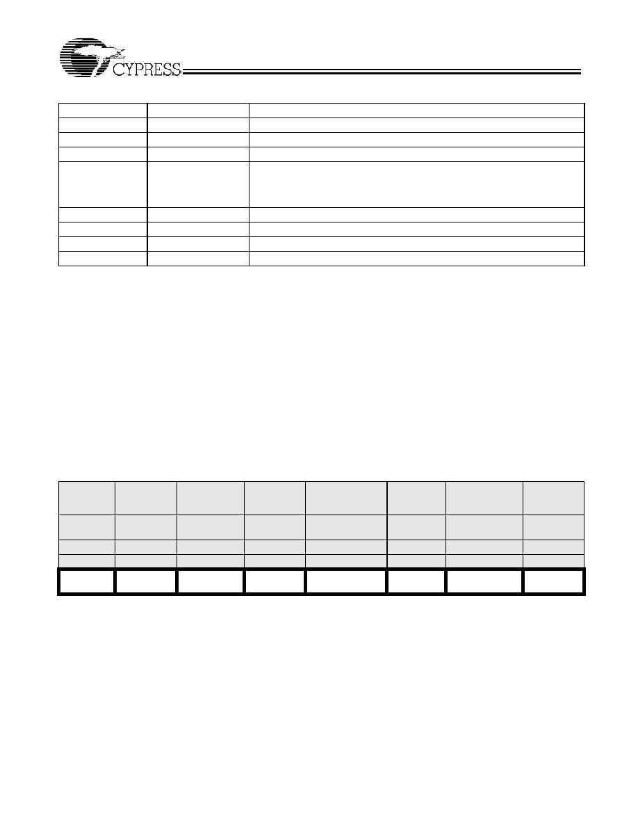
Table 1.
Pin
Function
Input
Frequency
Total Xtal
Load
Capacitance
Output
Frequency
Spread Percent
(0.5% 5%,
0.25% Intervals)
Reference
Output
Power-down or
Output Enable
Frequency
Modulation
Pin Name
XIN and
XOUT
XIN and XOUT
SSCLK
SSCLK
REFOUT
PD#/OE
SSCLK
Pin#
3 and 2
3 and 2
7
7
6
4
7
Unit
MHz
pF
MHz
%
On or Off
Select PD# or OE
kHz
Program
Value
ENTER DATA ENTER DATA
ENTER
DATA
ENTER DATA
ENTER
DATA
ENTER DATA
31.5

CY25100
Document #: 38-07499 Rev. *D
Page 3 of 11
Programming Description
Field-Programmable CY25100
The CY25100 is programmed at the package level, i.e., in a
programmer socket. The CY25100 is flash-technology based,
so the parts can be reprogrammed up to 100 times. This allows
for fast and easy design changes and product updates, and
eliminates any issues with old and out-of-date inventory.
Samples and small prototype quantities can be programmed
on the CY3672 programmer with CY3690 (TSSOP) or
CY3691 (SOIC) socket adapter.
CyberClocks
Online Software
CyberClocks
Online Software is a web-based software appli-
cation that allows the user to custom-configure the CY25100.
All the parameters in Table 1 given as "Enter Data" can be
programmed into the CY25100. CyberClocks Online outputs
an industry-standard JEDEC file used for programming the
CY25100. CyberClocksOnline is available at www.cyberclock-
sonline.com website through user registration. To register,
fillout the registration form and make sure to check the
"non-standard devices" box. For more information on the
registration process refer to CY3672 datasheet
For information regarding Spread Spectrum software
programming solutions, please contact your local Cypress
Sales or Field Application Engineer (FAE), representative for
details.
CY3672 FTG Programming Kit and CY3690/CY3691 Socket
Adapter
The Cypress CY3672 FTG programmer and CY3690/CY3691
Socket Adapter are needed to program the CY25100. The
CY3690 enables user to program CY25100ZCF and
CY25100ZIF (TSSOP) and CY3691 gives the user the ability
to program CY25100SCF and CY25100SIF (SOIC). Each
socket adapter comes with small prototype quantities of
CY25100. The CY3690/CY3691 is a separate orderable item,
so the existing users of the CY3672 FTG development kit or
CY3672-PRG programmer need to order only the socket
adapters to program the CY25100.
Factory-Programmable CY25100
Factory programming is available for volume manufacturing by
Cypress. All requests must be submitted to the local Cypress
Field Application Engineer (FAE) or sales representative. A
sample request form (refer to "CY25100 Sample Request
Form" at www.cypress.com) must be completed. Once the
request has been processed, you will receive a new part
number, samples, and data sheet with the programmed
values. This part number will be used for additional sample
requests and production orders.
Additional information on the CY25100 can be obtained from
the Cypress web site at www.cypress.com.
Product Functions
Input Frequency (XIN, pin 3 and XOUT
,
pin 2)
The input to the CY25100 can be a crystal or a clock. The input
frequency range for crystals is 8 to 30 MHz, and for clock
signals is 8 to 166 MHz.
C
XIN
and C
XOUT
(pin 3 and pin 2)
The load capacitors at Pin 1 (C
XIN
) and Pin 8 (C
XOUT
) can be
programmed from 12 pF to 60 pF with 0.5-pF increments. The
programmed value of these on-chip crystal load capacitors are
the same (XIN = XOUT = 12 to 60 pF).
The required values of C
XIN
and C
XOUT
can be calculated
using the following formula:
C
XIN
= C
XOUT
= 2C
L
C
P
where C
L
is the crystal load capacitor as specified by the
crystal manufacturer and C
P
is the parasitic PCB capacitance.
For example, if a fundamental 16-MHz crystal with C
L
of 16-pF
is used and C
P
is 2 pF, C
XIN
and C
XOUT
can be calculated as:
C
XIN
= C
XOUT
= (2 x 16) 2 = 30 pF.
If using a driven reference, set C
XIN
and
C
XOUT
to the
minimum value 12 pF.
Output Frequency, SSCLK Output (SSCLK, pin 7)
The modulated frequency at the SSCLK output is produced by
synthesizing the input reference clock. The modulation can be
stopped by SSON# digital control input (SSON# = HIGH, no
modulation). If modulation is stopped, the clock frequency is
the nominal value of the synthesized frequency without
modulation (spread % = 0). The range of synthesized clock is
from 3200 MHz.
Spread Percentage (SSCLK, pin 7)
The SSCLK spread can be programmed at any percentage
value from ±0.25% to ±2.5% for Center Spread and from
0.5% to 5.0% Down Spread.
Reference Output (REFOUT, pin 6)
The reference clock output has the same frequency and the
same phase as the input clock. This output can be
programmed to be enabled (clock on) or disabled (High-Z,
clock off). If this output is not needed, it is recommended that
users request the disabled (High-Z, Clock Off) option.
Frequency Modulation
The frequency modulation is programmed at 31.5 kHz for all
SSCLK frequencies from 3 to 200 MHz. Contact the factory if
a higher-modulation frequency is required.
Power-down or Output Enable (PD# or OE, pin 4):
The part can be programmed to include either PD# or OE
function. PD# function powers down the oscillator and PLL.
The OE function disables the outputs.
CY25100
Document #: 38-07499 Rev. *D
Page 4 of 11
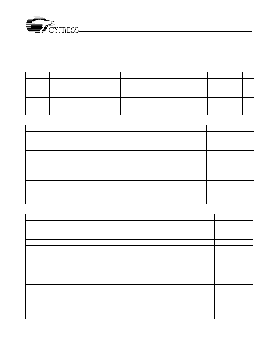
Absolute Maximum Rating
Supply Voltage (V
DD
) ........................................0.5 to +7.0V
DC Input Voltage...................................... 0.5V to V
DD
+ 0.5
Storage Temperature (Non-condensing).....55
°C to +125°C
Junction Temperature ................................ 40
°C to +125°C
Data Retention @ Tj = 125
°C................................> 10 years
Package Power Dissipation...................................... 350 mW
Static Discharge Voltage.......................................... > 2000V
(per MIL-STD-883, Method 3015)
Recommended Crystal Specifications
Parameter
Description
Comments
Min. Typ. Max. Unit
F
NOM
Nominal Crystal Frequency
Parallel resonance, fundamental mode, AT cut
8
30
MHz
C
LNOM
Nominal Load Capacitance
Internal load caps
6
30
pF
R
1
Equivalent Series Resistance (ESR)
Fundamental mode
25
R
3
/R
1
Ratio of Third Overtone Mode ESR to
Fundamental Mode ESR
Ratio used because typical R
1
values are much
less than the maximum spec
3
DL
Crystal Drive Level
No external series resistor assumed
0.5
2
mW
Operating Conditions
Parameter
Description
Min.
Typ.
Max.
Unit
V
DD
Supply Voltage
3.13
3.30
3.45
V
T
A
Ambient Commercial Temperature
0
70
°C
Ambient Industrial Temperature
40
85
°C
C
LOAD
Max. Load Capacitance @ pin 6 and pin 7
15
pF
F
ref
External Reference Crystal
(Fundamental tuned crystals only)
8
30
MHz
External Reference Clock
8
166
MHz
F
SSCLK
SSCLK output frequency, C
LOAD
= 15 pF
3
200
MHz
F
REFCLK
REFCLK output frequency, C
LOAD
= 15 pF
8
166
MHz
F
MOD
Spread Spectrum Modulation Frequency
30.0
31.5
33.0
kHz
T
PU
Power-up time for all VDDs to reach minimum spec-
ified voltage (power ramp must be monotonic)
0.05
500
ms
DC Electrical Characteristics
Parameter
Description
Condition
Min.
Typ.
Max.
Unit
I
OH
Output High Current
V
OH
= V
DD
0.5, V
DD
= 3.3V (source)
10
12
mA
I
OL
Output Low Current
V
OL
= 0.5, V
DD
= 3.3V (sink)
10
12
mA
V
IH
Input High Voltage
CMOS levels, 70% of V
DD
0.7V
DD
V
DD
V
V
IL
Input Low Voltage
CMOS levels, 30% of V
DD
0.3V
DD
V
I
IH
Input High Current, PD#/OE and
SSON# pins
V
in
= V
DD
10
µA
I
IL
Input Low Current, PD#/OE and
SSON# pins
V
in
= V
SS
10
µA
I
OZ
Output Leakage Current
Three-state output, PD#/OE = 0
10
10
µA
C
XIN
or C
XOUT
[1]
Programmable Capacitance at pin
2 and pin 3
Capacitance at minimum setting
12
pF
Capacitance at maximum setting
60
pF
C
IN
[1]
Input Capacitance at pin 4 and pin
8
Input pins excluding XIN and XOUT
5
7
pF
I
VDD
Supply Current
V
DD
= 3.45V, Fin = 30 MHz,
REFCLK = 30 MHz, SSCLK = 66 MHz,
C
LOAD
= 15 pF, PD#/OE = SSON# = V
DD
25
35
mA
I
DDS
Standby current
V
DD
= 3.45V, Device powered down with
PD# = 0V (driven reference pulled down)
15
30
µA
Notes:
1. Guaranteed by characterization, not 100% tested.
CY25100
Document #: 38-07499 Rev. *D
Page 5 of 11
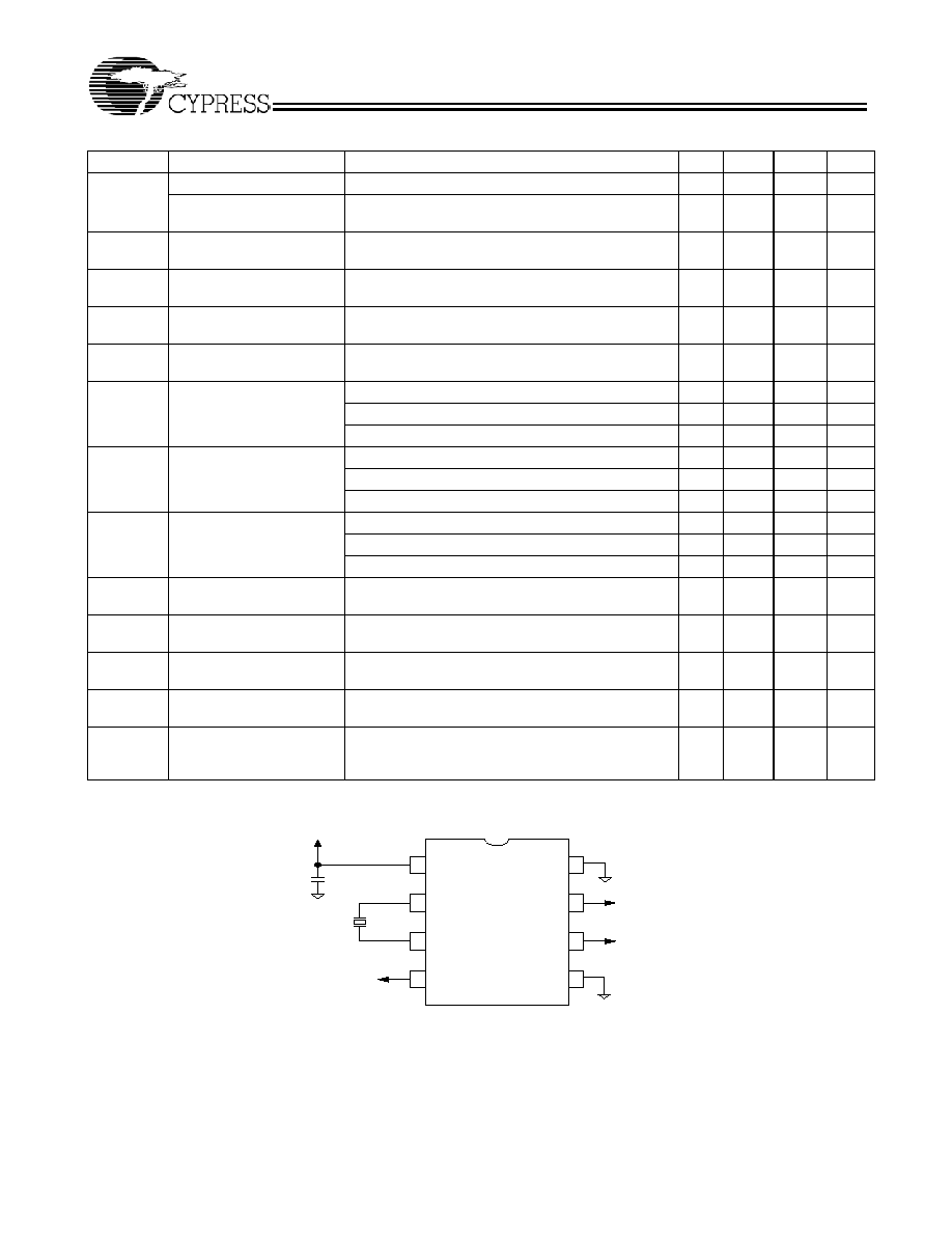
AC Electrical Characteristics
[1]
Parameter
Description
Condition
Min.
Typ.
Max.
Unit
DC
Output Duty Cycle
SSCLK, Measured at V
DD
/2
45
50
55
%
Output Duty Cycle
REFCLK, Measured at V
DD
/2
Duty Cycle of CLKIN = 50% at input bias
40
50
60
%
SR1
Rising Edge Slew Rate
SSCLK from 3 to 100 MHz; REFCLK from 3 to 100
MHz. 20%80% of V
DD
0.7
1.1
3.6
V/ns
SR2
Falling Edge Slew Rate
SSCLK from 3 to 100 MHz; REFCLK from 3 to 100
MHz. 80%20% of V
DD
0.7
1.1
3.6
V/ns
SR3
Rising Edge Slew Rate
SSCLK from 100 to 200 MHz; REFCLK from 100 to
166 MHz 20%80% of V
DD
1.2
1.6
4.0
V/ns
SR4
Falling Edge Slew Rate
SSCLK from 100 to 200 MHz; REFCLK from 100 to
166 MHz 80%20% of V
DD
1.2
1.6
4.0
V/ns
T
CCJ1
[2]
Cycle-to-Cycle Jitter
SSCLK (Pin 7)
CLKIN = SSCLK = 166 MHz, 2% spread, REFCLK off
90
120
ps
CLKIN = SSCLK = 66 MHz, 2% spread, REFCLK off
100
130
ps
CLKIN = SSCLK = 33 MHz, 2% spread, REFCLK off
130
170
ps
T
CCJ2
[2]
Cycle-to-Cycle Jitter
SSCLK (Pin 7)
CLKIN = SSCLK = 166 MHz, 2% spread, REFCLK on
100
130
ps
CLKIN = SSCLK = 66 MHz, 2% spread, REFCLK on
105
140
ps
CLKIN = SSCLK = 33 MHz, 2% spread, REFCLK on
200
260
ps
T
CCJ3
[2]
Cycle-to-Cycle Jitter
REFCLK (Pin 6)
CLKIN = SSCLK = 166 MHz, 2% spread, REFCLK on
80
100
ps
CLKIN = SSCLK = 66 MHz, 2% spread REFCLK on
100
130
ps
CLKIN = SSCLK = 33 MHz, 2% spread, REFCLK on
135
180
ps
t
STP
Power-down Time
(pin 4 = PD#)
Time from falling edge on PD# to stopped outputs
(Asynchronous)
150
350
ns
T
OE1
Output Disable Time
(pin 4 = OE)
Time from falling edge on OE to stopped outputs
(Asynchronous)
150
350
ns
T
OE2
Output Enable Time
(pin 4 = OE)
Time from rising edge on OE to outputs at a valid fre-
quency (Asynchronous)
150
350
ns
t
PU1
Power-up Time,
Crystal is used
Time from rising edge on PD# to outputs at valid fre-
quency (Asynchronous)
3.5
5
ms
t
PU2
Power-up Time,
Reference clock is used
Time from rising edge on PD# to outputs at valid fre-
quency (Asynchronous), reference clock at correct
frequency
2
3
ms
Application Circuit
[3, 4, 5]
2. Jitter is configuration dependent. Actual jitter is dependent on XIN jitter and edge rate, number of active outputs, output frequencies, spread percentage, temper-
ature, and output load. For more information, refer to the application note, "Jitter in PLL Based Systems: Causes, Effects, and Solutions" available at
http://www.cypress.com/clock/appnotes.html, or contact your local Cypress Field Application Engineer.
3. Since the load capacitors (C
XIN
and C
XOUT
) are provided by the CY25100, no external capacitors are needed on the XIN
and XOUT pins to match the crystal load
capacitor (C
L
). Only a single 0.1-
µF bypass capacitor is required on the V
DD
pin.
4. If an external clock is used, apply the clock to XIN (pin 3) and leave XOUT (pin 2) floating (unconnected).
5. If SSON# (pin 8) is LOW (V
SS
), the frequency modulation will be on at SSCLK pin (pin 7).
0 . 1 u F
V D D
1
3
2
4
5
6
7
8
V D D
X O U T
X I N / C L K I N
P D # / O E
V S S
R E F C L K
S S C L K
S S O N #
P o w e r
C Y 2 5 1 0 0