Spread Spectrum Clock Generator
CY25560
Cypress Semiconductor Corporation
∑
3901 North First Street
∑
San Jose
,
CA 95134
∑
408-943-2600
Document #: 38-07425 Rev. *D
Revised January 28, 2005
Features
∑ 25- to 100-MHz operating frequency range
∑ Wide (9) range of spread selections
∑ Accepts clock and crystal inputs
∑ Low power dissipation:
-- 56 mW @ Fin = 25 MHz
-- 89 mW @ Fin = 65 MHz
-- 139 mW @ Fin = 100 MHz
∑ Frequency spread disable function
∑ Center spread modulation
∑ Low cycle-to cycle jitter
∑ 8-pin SOIC package
∑ Commercial and Industrial temperature ranges
Applications
∑ Desktop, notebook, and tablet PCs
∑ VGA controllers
∑ LCD panels and monitors
∑ Printers and multifunction devices (MFP)
Benefits
∑ Peak electromagnetic interference (EMI) reduction by 8 to
16 dB
∑ Fast time to market
∑ Cost reduction
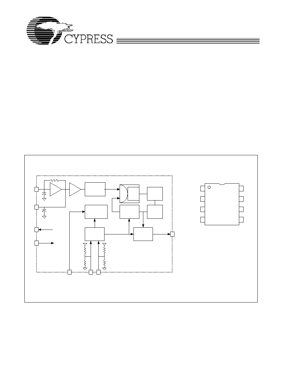
Block Diagram
Pin Configuration
VSS
PD
REFERENCE
DIVIDER
Loop
Filter
1
2
MODULATION
CONTROL
INPUT
DECODER
LOGIC
FEEDBACK
DIVIDER
vco
DIVIDER
&
MUX
8
3
CP
SSCLK
S0
S1
6
7
5
4
20 K
20 K
20 K
20 K
SSCC
VDD
Xout
Xin/
CLK
VDD
VDD
VSS
VSS
250 K
1
2
3
4
8
7
6
5
XIN/CLK
VDD
VSS
XOUT
S0
S1
SSCC
CY25560
SSCLK
CY25560
Document #: 38-07425 Rev. *D
Page 2 of 8
General Description
The Cypress CY25560 is a Spread Spectrum Clock Generator
(SSCG) IC used for the purpose of reducing EMI found in
today's high-speed digital electronic systems.
The CY25560 uses a Cypress proprietary phase-locked loop
(PLL) and Spread Spectrum Clock (SSC) technology to
synthesize and frequency modulate the input frequency of the
reference clock. By frequency modulating the clock, the
measured EMI at the fundamental and harmonic frequencies
of Clock (SSCLK) is greatly reduced.
This reduction in radiated energy can significantly reduce the
cost of complying with regulatory requirements and time to
market without degrading the system performance.
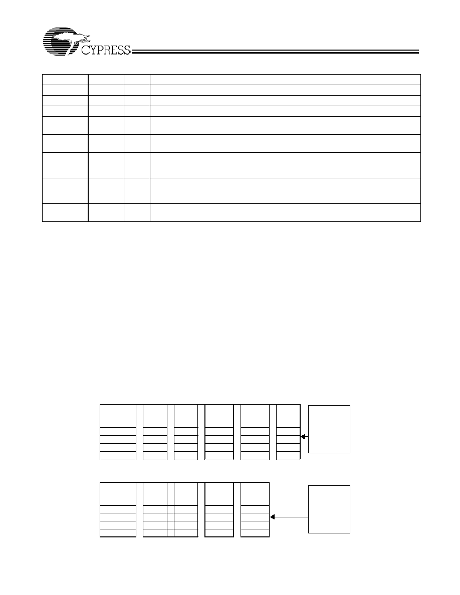
The CY25560 is a very simple and versatile device to use. The
frequency and spread% range is selected by programming S0
and S1 digital inputs. These inputs use three (3) logic states
including High (H), Low (L) and Middle (M) logic levels to select
one of the nine available Spread% ranges. Refer to Table 1 for
programming details.
The CY25560 is optimized for SVGA (40-MHz) and XVGA
(65-MHz) Controller clocks and also suitable for the applica-
tions where the frequency range is 25 to 100 MHz.
A wide range of digitally selectable spread percentages is
made possible by using three-level (High, Low, and Middle)
logic at the S0 and S1 digital control inputs.
The output spread (frequency modulation) is symmetrically
centered on the input frequency.
Spread Spectrum Clock Control (SSCC) function enables or
disables the frequency spread and is provided for easy
comparison of system performance during EMI testing.
The CY25560 is available in an eight-pin SOIC package with
0
∞C to 70∞C commercial and ≠40∞C to 85∞C Industrial
operating temperature ranges.
Pin Description
Pin Number Pin Name
Type
Pin Description
1
Xin/CLK
I
Clock or crystal connection input. Refer to Table 1 for input frequency range selection.
2
VDD
P
Positive power supply.
3
GND
P
Power supply ground.
4
SSCLK
O
Modulated clock output which is the same frequency as the input clock or the crystal
frequency.
5
SSCC
I
Spread Spectrum Clock Control (Enable/Disable) function. SSCG function is enabled
when input is HIGH and disabled when input is LOW. This pin is pulled HIGH internally.
6
S1
I
Tri-level logic input control pin used to select input frequency range and spread
percent. Refer to tri-level logic on page 3 for programming details. Pin 6 has internal resistor
divider network to V
DD
and V
SS
. Refer to Block Diagram on page 1.
7
S0
I
Tri-level logic input control pin used to select input frequency range and spread
percent. Refer to tri-level logic on page 3 for programming details. Pin 7 has internal resistor
divider network to V
DD
and V
SS
. Refer to Block Diagram on page 1.
8
Xout
O
Oscillator output pin connected to crystal. Leave this pin unconnected if an external
clock is used to drive X
IN
/CLK input (pin-1).
25 ≠ 50 MHz (Low Range)
Input
Frequency
(MHz)
S1=M
S0=M
(%)
S1=M
S0=0
(%)
S1=1
S0=0
(%)
S1=0
S0=0
(%)
S1=0
S0=M
(%)
25 ≠ 35
4.3 3.8 3.4 2.9 2.8
35 ≠ 40
3.9 3.5 3.1 2.5 2.4
40 ≠ 45
3.7 3.3 2.8 2.4 2.3
45 ≠ 50
3.4 3.1 2.6 2.2 2.1
50 ≠ 100 MHz (High Range)
Input
Frequency
(MHz)
S1=1
S0=M
(%)
S1=0
S0=1
(%)
S1=1
S0=1
(%)
S1=M
S0=1
(%)
50 ≠ 60
2.9 2.1 1.5 1.2
60 ≠ 70
2.8 2.0 1.4 1.1
70 ≠ 80
2.6 1.8 1.3 1.1
80 ≠ 100
2.4 1.7 1.2 1.0
Select the
Frequency and
Center Spread %
desired and then
set S1, S0 as
indicated.
Select the
Frequency and
Center Spread %
desired and then
set S1, S0 as
indicated.
Table 1. Frequency and Spread% Selection (Center Spread)
CY25560
Document #: 38-07425 Rev. *D
Page 3 of 8
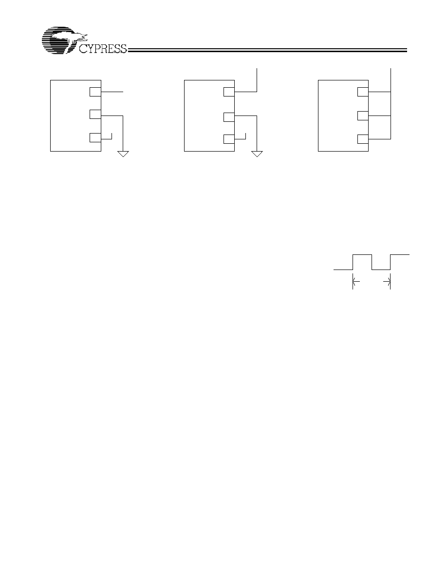
Tri-level Logic
With binary logic, four states can be programmed with two
control lines whereas three-level logic can program nine logic
states using two control lines. Three-level logic in the
CY25560 is implemented by defining a third logic state in
addition to the standard logic "1" and "0." Pins 6 and 7 of the
CY25560 recognize a logic state by the voltage applied to the
respective pin. These states are defined as "0" (Low), "M"
(Middle), and "1" (One). Each of these states have a defined
voltage range that is interpreted by the CY25560 as a "0", "M"
or "1" logic state. Refer to Table 2 for voltage ranges for each
logic state. The CY25560 has two equal value resistor dividers
connected internally to Pins 6 and 7 that produce the default
"M" (Middle) state if these pins are left unconnected (NC). Pins
6 and/or 7 can be tied directly to ground or V
DD
to program a
Logic "0" or "1" state, respectively.
SSCG Theory of Operation
The CY25560 is a PLL-type clock generator using a propri-
etary Cypress design. By precisely controlling the bandwidth
of the output clock, the CY25560 becomes a Low-EMI clock
generator. The theory and detailed operation of the CY25560
will be discussed in the following sections.
EMI
All digital clocks generate unwanted energy in their harmonics.
Conventional digital clocks are square waves with a duty cycle
that is very close to 50%. Because of this 50/50 duty cycle,
digital clocks generate most of their harmonic energy in the
odd harmonics, i.e., third, fifth, seventh, etc. It is possible to
reduce the amount of energy contained in the fundamental
and odd harmonics by increasing the bandwidth of the funda-
mental clock frequency. Conventional digital clocks have a
very high Q factor, which means that all of the energy at that
frequency is concentrated in a very narrow bandwidth, conse-
quently, higher energy peaks. Regulatory agencies test
electronic equipment by the amount of peak energy radiated
from the equipment. By reducing the peak energy at the funda-
mental and harmonic frequencies, the equipment under test is
able to satisfy agency requirements for EMI. Conventional
methods of reducing EMI have been to use shielding, filtering,
multilayer PCBs, etc. The CY25560 uses the approach of
reducing the peak energy in the clock by increasing the clock
bandwidth, and lowering the Q.
SSCG
SSCG uses a patented technology of modulating the clock
over a very narrow bandwidth and controlled rate of change,
both peak and cycle to cycle. The CY25560 takes a narrow
band digital reference clock in the range of 25≠100 MHz and
produces a clock that sweeps between a controlled start and
stop frequency and precise rate of change. To understand
what happens to a clock when SSCG is applied, consider a
65-MHz clock with a 50% duty cycle. From a 65-MHz clock we
know the following:
If this clock is applied to the Xin/CLK pin of CY25560, the
output clock at pin 4 (SSCLK) will be sweeping back and forth
between two frequencies. These two frequencies, F1 and F2,
are used to calculate to total amount of spread or bandwidth
applied to the reference clock at pin 1. As the clock is making
the transition from F1 to F2, the amount of time and sweep
waveform play a very important role in the amount of EMI
reduction realized from an SSCG clock.
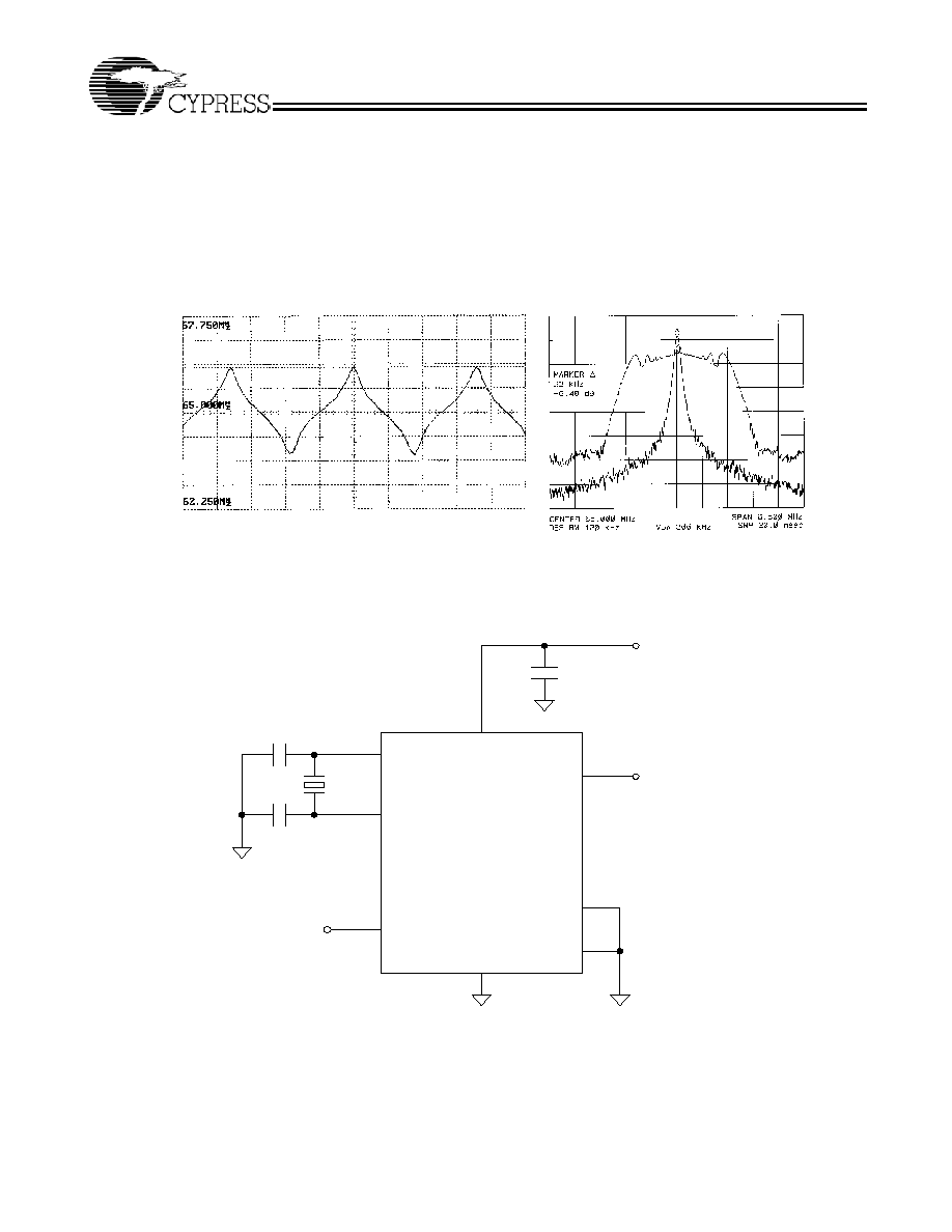
The modulation domain analyzer is used to visualize the
sweep waveform and sweep period. Figure 2 shows the
modulation profile of a 65 MHz SSCG clock. Notice that the
actual sweep waveform is not a simple sine or sawtooth
waveform. Figure 2 also shows a scan of the same SSCG
clock using a spectrum analyzer. In this scan you can see
a 6.48-dB reduction in the peak RF energy when using the
SSCG clock.
Modulation Rate
Spectrum Spread Clock Generators utilize frequency
modulation (FM) to distribute energy over a specific band of
frequencies. The maximum frequency of the clock (Fmax) and
minimum frequency of the clock (Fmin) determine this band of
frequencies. The time required to transition from Fmin to Fmax
and back to Fmin is the period of the Modulation Rate, Tmod.
Modulation Rates of SSCG clocks are generally referred to in
terms of frequency or Fmod = 1/Tmod.
The input clock frequency, Fin, and the internal divider count,
Cdiv, determine the Modulation Rate. In some SSCG clock
generators, the selected range determines the internal divider
count. In other SSCG clocks, the internal divider count is fixed
over the operating range of the part. The CY25560 has a fixed
divider count of 1166.
CY25560
CY25560
CY25560
7
6
5
VDD
S0 = "M" (N/C)
S1 = "0" (GND)
7
7
6
6
5
5
VDD
VDD
VDD
S0
S1
S0
S0
S1
S1
SSCC = "1"
SSCC = "1"
S1 = "0" (GND)
S0 = "1"
S0 = "1"
S1 = "1"
SSCC = "1"
Figure 1. Three-level Logic Examples
Clock Frequency = fc = 200 MHz
Clock Period = Tc =1/200 MHz = 5.0 ns.
Tc = 5.0 ns
50 %
50 %
CY25560
Document #: 38-07425 Rev. *D
Page 4 of 8
CY25560 Application Schematic
The schematic in Figure 3 above demonstrates how the
CY25560 is configured in a typical application. This application
is shown as using a 30-MHz fundamental crystal. In most
applications an external reference clock is used. Apply the
external clock signal at Xin (pin 1) and leave Xout (pin 8)
unconnected.
Contact Cypress if higher-order crystal is to be used.
Device
Cdiv
CY25560
1166
(All
Ranges)
Example:
Device
=
CY25560
Fin
=
65 MHz
Range =
S1 = 1, S0 = 0
Then;
Modulation Rate = Fmod = 65 MHz/1166 = 55.7 kHz.
Modulation Profile
Spectrum Analyzer
Figure 2. SSCG Clock, CY25560, Fin = 65 MHz
VDD
1
8
Y1
30 M H z
S S C C
VS S
S 1
S 0
X IN /C LK
X O U T
S S C LK
V D D
CY25560
5
7
6
4
0.1 uF
C3
C2
C 3
27 pF
27 pF
2
3
VDD
Figure 3. Application Schematic
CY25560
Document #: 38-07425 Rev. *D
Page 5 of 8
Absolute Maximum Ratings (Commercial Grade)
[1, 2]
Supply Voltage (V
DD
): .................................... ≠0.5V to +6.0V
DC Input Voltage:....................................≠0.5V to VDD+0.5V
Junction Temperature .................................≠40∞C to +140∞C
Operating Temperature: ...................................... 0∞C to 70∞C
Storage Temperature.................................. ≠65∞C to +150∞C
Static Discharge Voltage(ESD)............................ 2,000V-Min
Notes:
1. Operation at any Absolute Maximum Rating is not implied.
2. Single Power Supply: The voltage on any input or I/O pin cannot exceed the power pin during power up.
DC Electrical Characteristics V
DD
= 3.3V±10%, T= 0∞C to 70∞C and C
L
(Pin 4) = 15 pF, unless otherwise noted
Parameter
Description
Conditions
Min.
Typ.
Max.
Unit
V
DD
Power Supply Range
±10%
2.97
3.3
3.63
V
V
IH
Input High Voltage
S0 and S1 only
0.85V
DD
V
DD
V
DD
V
V
IM
Input Middle Voltage
S0 and S1 only
0.40V
DD
0.50V
DD
0.60V
DD
V
V
IL
Input Low Voltage
S0 and S1 only
0.0
0.0
0.15V
DD
V
V
OH
Output High Voltage
I
OH
= 6 ma
2.4
V
V
OL
Output Low Voltage
I
OH
= 6 ma
0.4
V
C
in1
Input Capacitance
Xin/CLK (Pin 1)
3
4
5
pF
C
in2
Input Capacitance
Xout (Pin 8)
6
8
10
pF
C
in2
Input Capacitance
S0, S1, SSCC (Pins 7, 6, 5)
3
4
5
pF
I
DD1
Power Supply Current
FIN = 25 MHz, CL= 0
17
23
mA
I
DD2
Power Supply Current
FIN = 65 MHz, CL= 0
27
41
mA
I
DD3
Power Supply Current
FIN = 100 MHz, CL= 0
42
59
mA
Table 2. Electrical Timing Characteristics V
DD
= 3.3V±10%, T= 0∞C to 70∞C and C
L
(Pin 4) = 15 pF, unless otherwise noted
Parameter
Description
Conditions
Min.
Typ.
Max.
Unit
I
CLKFR
Input Clock Frequency Range
V
DD
= 3.30V
25
100
MHz
t
F
Clock Rise Time (Pin 4)
SSCLK @ 0.4 ≠ 2.4V
1.0
1.8
2.8
ns
t
R
Clock Fall Time (Pin 4)
SSCLK @ 0.4 ≠ 2.4V
1.0
1.8
2.8
ns
D
TYin
Input Clock Duty Cycle
XIN/CLK (Pin 1)
25
50
75
%
D
TYout
Output Clock Duty Cycle
SSCLK (Pin 4)
45
50
55
%
J
CC1
Cycle-to-Cycle Jitter
Fin = 25≠50 MHz, SSCC = 1
150
300
ps
J
CC2
Cycle-to-Cycle Jitter
Fin = 50≠100 MHz, SSCC = 1
130
200
ps
CY25560
Document #: 38-07425 Rev. *D
Page 6 of 8
Absolute Maximum Conditions (Industrial Grade)
[1, 2]
Supply Voltage (V
DD
): .................................... ≠0.5V to +6.0V
DC Input Voltage:....................................≠0.5V to VDD+0.5V
Junction Temperature .................................≠40∞C to +140∞C
Operating Temperature:.................................. ≠40∞C to 85∞C
Storage Temperature.................................. ≠65∞C to +150∞C
Static Discharge Voltage(ESD)............................ 2,000V-Min
Table 3. DC Electrical Characteristics (Preliminary) V
DD
= 3.3V±10%, T= ≠40∞C to 85∞C and C
L
(Pin 4) = 15 pF, unless
otherwise noted
Parameter
Description
Conditions
Min.
Typ.
Max.
Unit
V
DD
Power Supply Range
±10%
2.97
3.3
3.63
V
V
IH
Input High Voltage
S0 and S1 only
0.85V
DD
V
DD
V
DD
V
V
IM
Input Middle Voltage
S0 and S1 only
0.40V
DD
0.50V
DD
0.60V
DD
V
V
IL
Input Low Voltage
S0 and S1 only
0.0
0.0
0.15V
DD
V
V
OH
Output High Voltage
I
OH
= 6 ma
2.2
V
V
OL
Output Low Voltage
I
OH
= 6 ma
0.4
V
C
in1
Input Capacitance
Xin/CLK (Pin 1)
3
4
5
pF
C
in2
Input Capacitance
Xout (Pin 8)
6
8
10
pF
C
in2
Input Capacitance
S0, S1, SSCC (Pins 7, 6, 5)
3
4
5
pF
I
DD1
Power Supply Current
FIN = 25 MHz, CL= 0
17
24
mA
I
DD2
Power Supply Current
FIN = 65 MHz, CL= 0
27
41
mA
I
DD3
Power Supply Current
FIN = 100 MHz, CL= 0
42
61
mA
Table 4. Electrical Timing Characteristics (Preliminary) V
DD
= 3.3V±10%, T= ≠40∞C to 85∞C and C
L
(Pin 4) = 15 pF, unless
otherwise noted
Parameter
Description
Conditions
Min.
Typ.
Max.
Unit
I
CLKFR
Input Clock Frequency Range
V
DD
= 3.30V
25
100
MHz
t
F
Clock Rise Time (Pin 4)
SSCLK @ 0.4 ≠ 2.4V
1.0
1.8
3.0
ns
t
R
Clock Fall Time (Pin 4)
SSCLK @ 0.4 ≠ 2.4V
1.0
1.8
3.0
ns
D
TYin
Input Clock Duty Cycle
XIN/CLK (Pin 1)
25
50
75
%
D
TYout
Output Clock Duty Cycle
SSCLK (Pin 4)
45
50
55
%
J
CC1
Cycle-to-Cycle Jitter
Fin = 25≠50 MHz, SSCC = 1
150
300
ps
J
CC2
Cycle-to-Cycle Jitter
Fin = 50≠100 MHz, SSCC = 1
130
200
ps
Ordering Information
Part Number
Package Type
Product Flow
CY25560SC
8-pin SOIC
Commercial, 0
∞C to 70∞C
CY25560SCT
8-pin SOIC≠Tape and Reel
Commercial, 0
∞C to 70∞C
CY25560SI
8-pin SOIC
Industrial, ≠40
∞C to 85∞C
CY25560SIT
8-pin SOIC≠Tape and Reel
Industrial, ≠40
∞C to 85∞C
Lead-free
CY25560SXC
8-pin SOIC
Commercial, 0
∞C to 70∞C
CY25560SXCT
8-pin SOIC≠Tape and Reel
Commercial, 0
∞C to 70∞C
CY25560SXI
8-pin SOIC
Industrial, ≠40
∞C to 85∞C
CY25560SXIT
8-pin SOIC≠Tape and Reel
Industrial, ≠40
∞C to 85∞C
CY25560
Document #: 38-07425 Rev. *D
Page 7 of 8
© Cypress Semiconductor Corporation, 2005. The information contained herein is subject to change without notice. Cypress Semiconductor Corporation assumes no responsibility for the use
of any circuitry other than circuitry embodied in a Cypress product. Nor does it convey or imply any license under patent or other rights. Cypress products are not warranted nor intended to be
used for medical, life support, life saving, critical control or safety applications, unless pursuant to an express written agreement with Cypress. Furthermore, Cypress does not authorize its
products for use as critical components in life-support systems where a malfunction or failure may reasonably be expected to result in significant injury to the user. The inclusion of Cypress
products in life-support systems application implies that the manufacturer assumes all risk of such use and in doing so indemnifies Cypress against all charges.
Package Drawing and Dimensions
All product and company names mentioned in this document are the trademarks of their respective holders.
SEATING PLANE
PIN 1 ID
0.230[5.842]
0.244[6.197]
0.157[3.987]
0.150[3.810]
0.189[4.800]
0.196[4.978]
0.050[1.270]
BSC
0.061[1.549]
0.068[1.727]
0.004[0.102]
0.0098[0.249]
0.0138[0.350]
0.0192[0.487]
0.016[0.406]
0.035[0.889]
0.0075[0.190]
0.0098[0.249]
1. DIMENSIONS IN INCHES[MM] MIN.
MAX.
0∞~8∞
0.016[0.406]
0.010[0.254]
X 45∞
2. PIN 1 ID IS OPTIONAL,
ROUND ON SINGLE LEADFRAME
RECTANGULAR ON MATRIX LEADFRAME
0.004[0.102]
8 Lead (150 Mil) SOIC S08
1
4
5
8
3. REFERENCE JEDEC MS-012
PART #
S08.15 STANDARD PKG.
SZ08.15 LEAD FREE PKG.
4. PACKAGE WEIGHT 0.07gms
8-lead (150-Mil) SOIC S8
51-85066-*C
CY25560
Document #: 38-07425 Rev. *D
Page 8 of 8
Document History Page
Document Title:CY25560 Spread Spectrum Clock Generator
Document Number: 38-07245
Rev.
ECN No.
Issue Date
Orig. of
Change
Description of Change
**
115261
06/12/02
OXC
New Data Sheet
*A
119441
10/17/02
RGL
Corrected the values in the Absolute Maximum Ratings to match the device.
*B
122704
12/30/02
RBI
Added power up requirements to maximum ratings information.
*C
125549
05/15/03
RGL
Added Industrial Temperature Range to the device.
Removed V
OL2
and V
OH2
spec in the DC specs table
Changed IDD Values from 11/17/25 typ and 14/22/34max to 17/27/42 typ
and 23/41/59 max
Changed T
F
/T
R
values from 1.3/1.3 typ and 1.6/1.6 max to 1.8/1.8 typ and
2.8/2.8 max in the Electrical Char. table.
Changed J
CC1/2
values from 200/250 typ and 250/300 max to 150/130 typ
to 300/200 max in the Electrical Char. table.
Changed the low power dissipation from 36/56/82mW to 56/89/139mW
respectively.
Changed the low cycle-to-cycle jitter from 195/175/100ps-typ to
450/225/150 ps-max
*D
314293
See ECN
RGL
Added Lead-free devices