Äîêóìåíòàöèÿ è îïèñàíèÿ www.docs.chipfind.ru
Programmable High-Frequency Crystal Oscillator
with Spread Spectrum (SSXO)
CY25701
Cypress Semiconductor Corporation
·
3901 North First Street
·
San Jose
,
CA 95134
·
408-943-2600
Document #: 38-07684 Rev. *B
Revised October 15, 2004
Features
· Crystal Oscillator with Spread Spectrum Clock (SSC)
· Wide operating output (SSCLK) frequency range
· 10166 MHz
· Programmable spread spectrum with nominal 31.5 kHz
modulation frequency
· Center spread: ±0.25% to ±2.0%
· Down spread: 0.5% to 4.0%
· Integrated phase-locked loop (PLL)
· Low cycle-to-cycle Jitter
· 3.3V operation
· Output Enable function
· Package available in 4-Lead Plastic JE SMD
Benefits
· Provides wide range of spread percentages for
maximum electromagnetic interference (EMI)
reduction, to meet regulatory agency electromagnetic
compliance (EMC) requirements. Reduces devel-
opment and manufacturing costs and time-to-market.
· Eliminates the need for external crystal oscillator.
· Internal PLL to generate up to 166 MHz output.
· Suitable for most PC, consumer, and networking
applications.
· Application compatibility in standard and low-power
systems.
· In-house programming of samples and prototype
quantities is available using the CY3672 programming
kit and CY3613 socket adapter. Production quantities
are available through Cypress's value-added distri-
bution partners or by using third-party programmers
from BP Microsystems, HiLo Systems, and others.
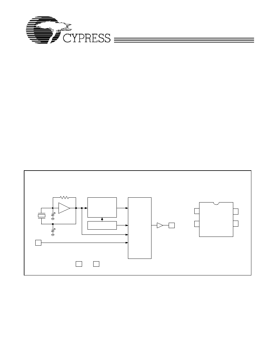
Logic Block Diagram
PLL
with
MODULATION
CONTROL
PROGRAMMABLE
CONFIGURATION
OUTPUT
DIVIDERS
and
MUX
1
4
2
VDD
VSS
OE
RFB
C
XOUT
C
XIN
3
SSCLK
Pin Configuration
CY25701
4-pin Plastic SMD
4
OE
3
VDD
1
2
VSS
SSCLK
CY25701
Document #: 38-07684 Rev. *B
Page 2 of 7
Functional Description
The CY25701 is a Spread Spectrum Crystal Oscillator (SSXO)
IC used for the purpose of reducing EMI found in today's
high-speed digital electronic systems.
The device uses a Cypress proprietary PLL and Spread
Spectrum Clock (SSC) technology to synthesize and modulate
the frequency of the embedded input crystal. By frequency
modulating the clock, the measured EMI at the fundamental
and harmonic frequencies are greatly reduced. This reduction
in radiated energy can significantly reduce the cost of
complying with regulatory agency (EMC) requirements and
improve time-to-market without degrading system perfor-
mance.
The CY25701 uses a programmable configuration memory
array to synthesize output frequency and spread%.
The spread% is programmed to either center spread or down
spread with various spread percentages. The range for center
spread is from ±0.25% to ±2.00%. The range for down spread
is from 0.5% to 4.0%. Contact the factory for smaller or
larger spread% amounts if required. Refer to Table 2 for
spread selection values.
The frequency modulated SSCLK output can be programmed
from 10166 MHz.
The CY25701 is available in a 4-pin plastic SMD package with
operating temperature range of 20 to 70°C.
Programming Description
Field/Factory-Programmable CY25701
Field/Factory programming is available for samples and
manufacturing by Cypress and its distributors. All requests
must be submitted to the local Cypress Field Application
Engineer (FAE) or sales representative. Once the request has
been processed, you will receive a new part number, samples,
and data sheet with the programmed values. This part number
will be used for additional sample requests and production
orders.
Additional information on the CY25701 can be obtained from
the Cypress web site at www.cypress.com.
Output Frequency, SSCLK Output (SSCLK, pin 3)
The modulated frequency at the SSCLK output is produced by
synthesizing the embedded crystal oscillator frequency input.
The range of synthesized clock is from 10166 MHz.
Spread Percentage (SSCLK, pin 3)
The SSCLK spread can be programmed to various spread
percentage values from ±0.25% to ±2.0% for Center Spread
and from 0.5% to 4.0% for Down Spread. Refer to Table 2
for available spread options
Frequency Modulation (SSCLK, pin 3)
The frequency modulation is programmed at 31.5 kHz for all
SSCLK frequencies from 10 to 166 MHz. Contact the factory
if a higher-modulation frequency is required.
Pin Definition
Pin
Name
Description
1
OE
Output Enable pin: Active HIGH. If OE = 1, SSCLK is enabled.
2
VSS
Power supply ground.
3
SSCLK
Spread spectrum clock output.
4
VDD
3.3V power supply.
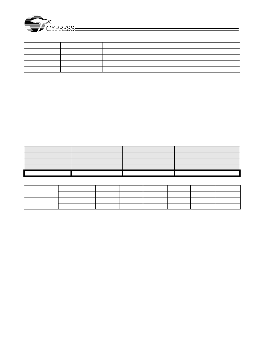
Table 1. Programming Data Requirement
Pin Function
Output Frequency
Spread Percent Code
Frequency Modulation
Pin Name
SSCLK
SSCLK
SSCLK
Pin#
3
3
3
Units
MHz
%
kHz
Program Value
ENTER DATA
ENTER DATA
31.5
Table 2. Spread Percent Selection
Center Spread
Code
A
B
C
D
E
F
Percentage
±0.25%
±0.5%
±0.75%
±1.0%
±1.5%
±2.0%
Down Spread
Code
G
H
J
K
L
M
Percentage
0.5%
1.0%
1.5%
2.0%
3.0%
4.0%
CY25701
Document #: 38-07684 Rev. *B
Page 3 of 7
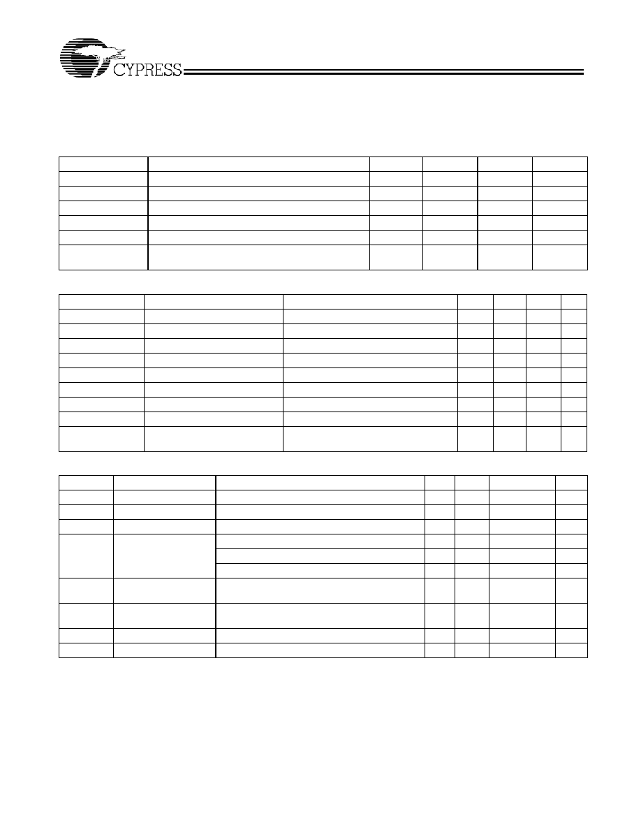
Absolute Maximum Rating
Supply Voltage (VDD) .................................... 0.5V to +7.0V
DC Input Voltage....................................0.5V to V
DD
+ 0.5V
Storage Temperature (Non-condensing) .... 55°C to +100°C
Junction Temperature ................................ 40°C to +125°C
Data Retention @ Tj = 125
°C................................> 10 years
Package Power Dissipation...................................... 350 mW
Operating Conditions
Parameter
Description
Min.
Typ.
Max.
Unit
V
DD
Supply Voltage
3.00
3.30
3.60
V
T
A
Ambient Temperature
20
70
°C
C
LOAD
Max. Load Capacitance @ pin 3
15
pF
F
SSCLK
SSCLK output frequency, C
LOAD
= 15 pF
10
166
MHz
F
MOD
Spread Spectrum Modulation Frequency
30.0
31.5
33.0
kHz
T
PU
Power-up time for VDD to reach minimum specified
voltage (power ramp must be monotonic)
0.05
500
ms
DC Electrical Characteristics
Parameter
Description
Condition
Min.
Typ.
Max.
Unit
I
OH
Output High Current (pin 3)
V
OH
= V
DD
0.5, V
DD
= 3.3V (source)
10
12
mA
I
OL
Output Low Current (pin 3)
V
OL
= 0.5, V
DD
= 3.3V (sink)
10
12
mA
V
IH
Input High Voltage (pin 1)
CMOS levels, 70% of V
DD
0.7V
DD
V
DD
V
V
IL
Input Low Voltage (pin 1)
CMOS levels, 30% of V
DD
0.3V
DD
V
I
IH
Input High Current (pin 1)
V
in
= V
DD
10
µA
I
IL
Input Low Current (pin 1)
V
in
= V
SS
10
µA
I
OZ
Output Leakage Current (pin 3) Three-state output, OE = 0
10
10
µA
C
IN
[1]
Input Capacitance (pin 1)
Pin 1, or OE
5
7
pF
I
VDD
Supply Current
V
DD
= 3.3V, SSCLK = 10 to 166 MHz,
C
LOAD
= 0, OE = V
DD
30
mA
AC Electrical Characteristics
[1]
Parameter
Description
Condition
Min.
Typ.
Max.
Unit
DC
Output Duty Cycle
SSCLK, Measured at V
DD
/2
45
50
55
%
t
R
Output Rise Time
20%80% of V
DD,
C
L
= 15pF
2.7
ns
t
F
Output Fall Time
20%80% of V
DD,
C
L
= 15pF
2.7
ns
T
CCJ1
[2]
Cycle-to-Cycle Jitter
SSCLK (Pin 3)
SSCLK
133 MHz, Measured at V
DD
/2
200
ps
25 MHz
SSCLK <133 MHz, Measured at V
DD
/2
400
ps
SSCLK < 25 MHz, Measured at V
DD
/2
1% of 1/SSCK
s
T
OE1
Output Disable Time
(pin1 = OE)
Time from falling edge on OE to stopped outputs
(Asynchronous)
150
350
ns
T
OE2
Output Enable Time
(pin1 = OE)
Time from rising edge on OE to outputs at a valid
frequency (Asynchronous)
150
350
ns
T
LOCK
PLL Lock Time
Time for SSCLK to reach valid frequency
10
ms
f
Aging in Frequency
T
A
= 25°C, First year
5
5
ppm
Notes:
1. Guaranteed by characterization, not 100% tested.
2. Jitter is configuration dependent. Actual jitter is dependent on output frequencies, spread percentage, temperature, and output load. For more information, refer
to the application note, "Jitter in PLL Based Systems: Causes, Effects, and Solutions" available at http://www.cypress.com/clock/appnotes.html, or contact your
local Cypress Field Application Engineer.
CY25701
Document #: 38-07684 Rev. *B
Page 4 of 7
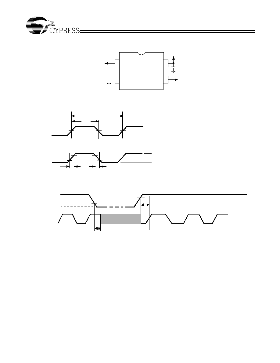
Application Circuit
Switching Waveforms
0.1uF
VDD
1
2
3
4
OE
VSS
SSCLK
VDD
Power
CY25701
Duty Cycle Timing (DC = t
1A
/t
1B
)
t
1A
t
1B
SSCLK
Output Rise/Fall Time
SSCLK
Tr
V
DD
0V
Tf
Output Rise time (Tr) = (0.6 x V
DD
)/SR1 (or SR3)
Output Fall time (Tf) = (0.6 x V
DD
)/SR2 (or SR4)
Refer to AC Electrical Characteristics table for SR (Slew Rate) values.
Output Enable/Disable Timing
SSCLK
V
DD
T
OE1
V
IL
V
IH
OUTPUT
ENABLE
0V
(Asynchronous
)
High Impedance
T
OE2
CY25701
Document #: 38-07684 Rev. *B
Page 5 of 7
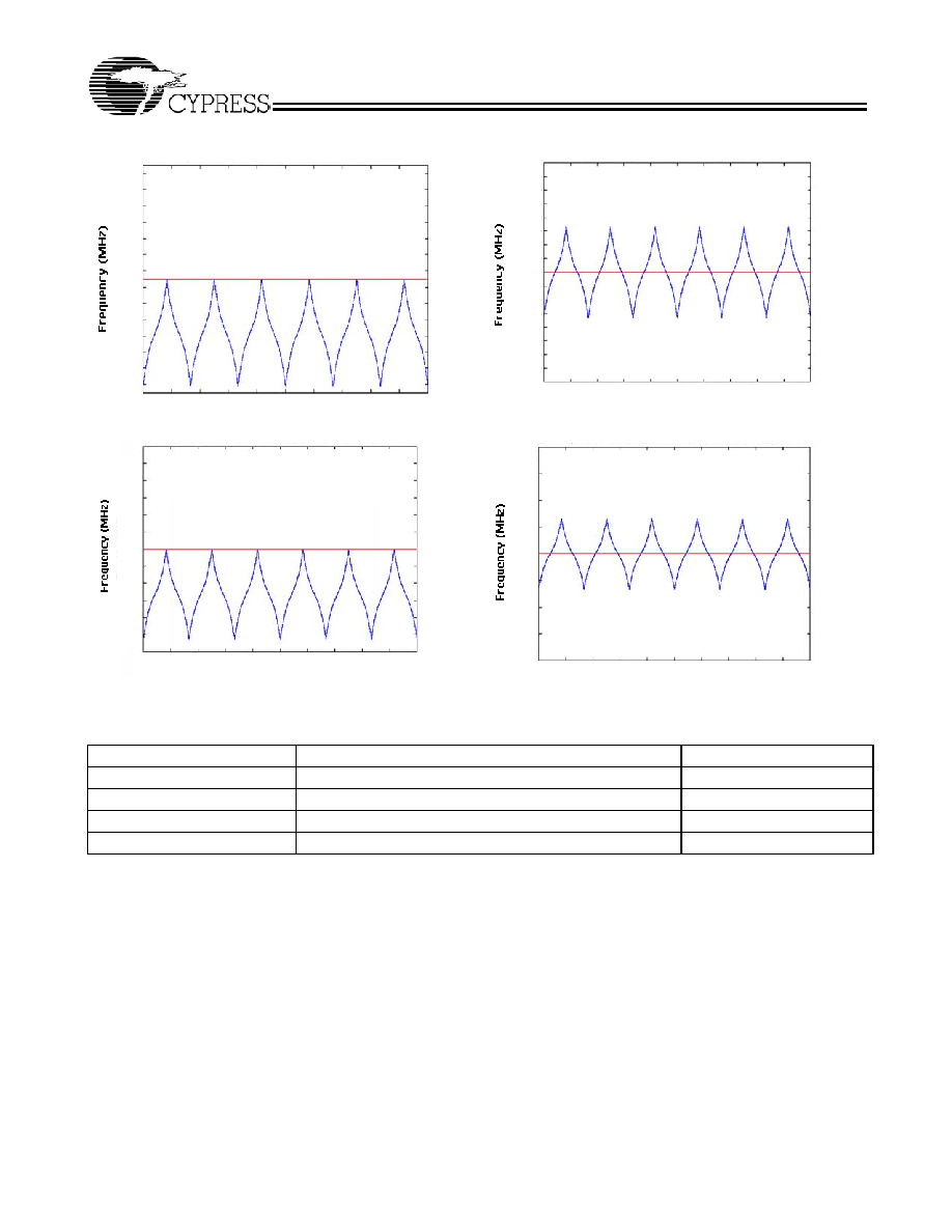
Informational Graphs
[3]
Spread Spectrum Profile: Fnom=166MHz,
Fmod=30kHz, Spread%= -4%
172.5
171.5
170.5
169.5
168.5
167.5
166.5
165.5
164.5
163.5
162.5
161.5
160.5
159.5
Fnominal
0 20 40 60 80 100 120 140 160 180 200
Time (us)
Spread Spectrum Profile: Fnom=166MHz,
Fmod=30kHz, Spread%= +/-1%
0 20 40 60 80 100 120 140 160 180 200
Time (us)
Fnominal
169.5
169
168.5
168
167.5
167
166.5
166
165.5
165
164.5
164
163.5
163
162.5
Spread Spectrum Profile: Fnom=66MHz,
Fmod=30kHz, Spread%= -4%
0 20 40 60 80 100 120 140 160 180 200
Time (us)
Fnominal
68.5
68
67.5
67
66.5
66
65.5
65
64.5
64
63.5
Spread Spectrum Profile: Fnom=66MHz,
Fmod=30kHz, Spread%= +/-1%
0 20 40 60 80 100 120 140 160 180 200
Time (us)
Fnominal
67.5
67
66.5
66
65.5
65
64.5
Ordering Information
Part Number
[4,5]
Package description
Product Flow
CY25701JXCZZZZ
4-Lead Plastic JE SMD Lead-free
Commercial, 20° to 70°C
CY25701JXCZZZZT
4-Lead Plastic JE SMD, Tape and Reel Lead-free
Commercial, 20° to 70°C
CY25701FJXC
4-Lead Plastic JE SMD Lead-free
Commercial, 20° to 70°C
CY25701FJXCT
4-Lead Plastic JE SMD, Tape and Reel Lead-free
Commercial, 20° to 70°C
Notes:
3. The "Informational Graphs" are meant to convey the typical performance levels. No performance specifications is implied or guaranteed. Refer to the tables on
pages 4 and 5 for device specifications.
4. "ZZZZ" denotes the assigned product dash number. This number will be assigned by factory after the output frequency and spread percent programming data
is received from the customer.
5. "FJXC" suffix is used for products programmed in field by Cypress distributors.