Äîêóìåíòàöèÿ è îïèñàíèÿ www.docs.chipfind.ru
Programmable High-Frequency Crystal Oscillator (XO)
CY25702
Cypress Semiconductor Corporation
·
3901 North First Street
·
San Jose
,
CA 95134
·
408-943-2600
Document #: 38-07721 Rev. **
Revised December 09, 2004
Features
· Programmable High-frequency Crystal Oscillator (XO)
· Wide output (CLK) range from:
-- 1.0 to 125 MHz (V
DD
= 5.0V)
-- 1.0 to 90 MHz (V
DD
= 3.3V)
· Integrated phase-locked loop (PLL)
· Low cycle-to-cycle Jitter
· 3.3/5.0V operation
· Output Enable function
· Power-down function
· Refer to CY25701 for SSCG function
· Lead-free package
Benefits
· Eliminates the need for external crystal oscillator.
· Internal PLL to generate up to 125-MHz output.
· Suitable for most PC, consumer and networking
applications.
· Application compatibility in standard and low-power
systems.
· CY25701 can be used as a direct replacement in 3.3V
applications if Spread Spectrum Clock (SSC) is
required for EMI reduction without any PCB
modification.
· In-house programming of samples and prototype
quantities is available using the CY3672 programming
kit and CY36xx socket adapter. Sample and production
quantities are available through Cypress's value-added
distribution partners.
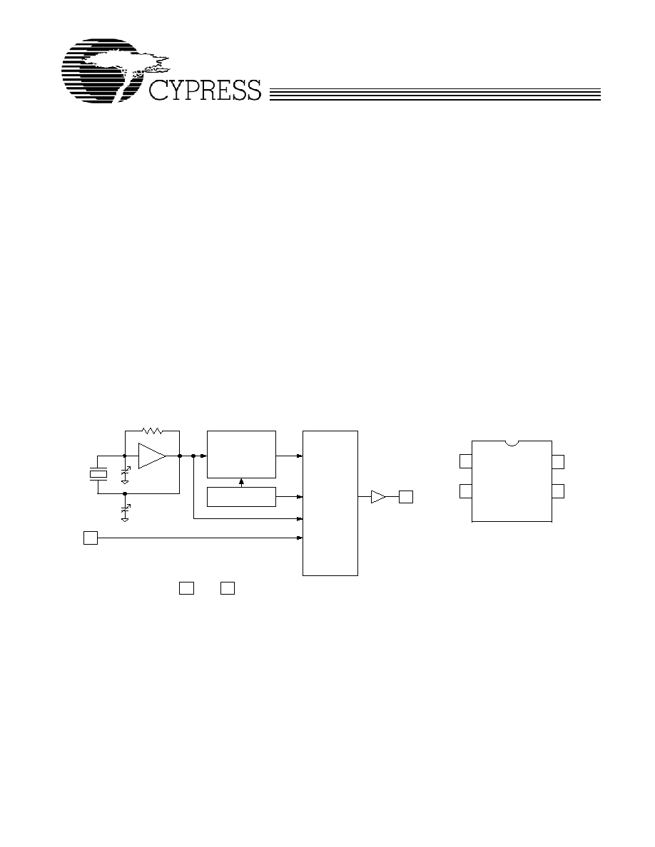
Logic Block Diagram
PLL
PROGRAMMABLE
CONFIGURATION
OUTPUT
DIVIDERS
and
MUX
1
4
2
VDD
VSS
OE/PD#
RFB
C
XOUT
C
XIN
3
CLK
Pin Configuration
CY25702
4-pin Plastic SMD
4
OE/PD#
3
VDD
1
2
VSS
CLK
CY25702
Document #: 38-07721 Rev. **
Page 2 of 7
Functional Description
The CY25702 is a Crystal Oscillator (XO).
The device uses a Cypress proprietary PLL to synthesize the
frequency of the embedded input crystal.
The CY25702 uses a programmable configuration memory
array to synthesize output frequency.
The frequency CLK output can be programmed from 10125
MHz.
The CY25702 is available in a 4-pin plastic SMD packages
with operating temperature range of 20 to 70°C.
Programming Description
Field/Factory-Programmable CY25702
Field/Factory programming is available for samples and
manufacturing by Cypress and its distributors. All requests
must be submitted to the local Cypress Field Application
Engineer (FAE) or sales representative. Once the request has
been processed, you will receive a new part number, samples,
and data sheet with the programmed values. This part number
will be used for additional sample requests and production
orders.
Additional information on the CY25702 can be obtained from
the Cypress web site at www.cypress.com.
Output Frequency, CLK Output (CLK, pin 3)
The frequency at the CLK output is produced by synthesizing
the embedded crystal oscillator frequency input. The range of
synthesized clock is from 1125MHz when VDD= 5V and
190MHz when VDD = 3.3V.
Output Enable or Power Down (OE/PD#, pin 1)
Pin 1 can be programmed as either output enable (OE) or
Power Down (PD#).
Absolute Maximum Rating
Supply Voltage (VDD).....................................0.5V to +7.0V
DC Input Voltage ................................... 0.5V to V
DD
+ 0.5V
Storage Temperature (Non-condensing) .... 55°C to +100°C
Junction Temperature ................................ 40°C to +125°C
Data Retention @ Tj = 125
°C................................> 10 years
Package Power Dissipation...................................... 350 mW
Pin Definition
Pin
Name
Description
1
OE/PD#
Output Enable pin: Active HIGH. If OE = 1, CLK is enabled.
Power Down pin: Active LOW. If PD# = 0, Power Down is enabled.
2
VSS
Power supply ground.
3
CLK
Clock output.
4
VDD
3.3V or 5.0V power supply.
Table 1. Programming Data Requirement
Pin Function
Output Frequency
Output Enable/Power Down
Power Supply
Pin Name
CLK
OE/PD#
VDD
Pin#
3
1
4
Units
MHz
N/A
V
Program Value
ENTER DATA
ENTER DATA
ENTER DATA
Operating Conditions
Parameter
Description
Min.
Typ.
Max.
Unit
V
DD1
Supply Voltage Range
3.00
3.30
3.60
V
V
DD2
Supply Voltage Range
4.50
5.00
5.50
V
T
A
Ambient Temperature
20
70
°C
C
LOAD
Max. Load Capacitance @ pin 3
15
pF
F
CLK1
CLK output frequency, C
LOAD
= 15 pF, VDD = 5.0V
1.0
125
MHz
F
CLK2
CLK output frequency, C
LOAD
= 15 pF, , VDD = 3.3V
1.0
90
MHz
T
PU
Power-up time for VDD to reach minimum specified
voltage (power ramp must be monotonic)
0.05
500
ms
DC Electrical Characteristics
Parameter
Description
Condition
Min.
Typ.
Max.
Unit
V
OH1
High Output Voltage
V
DD
= 5.0V, I
OH
= 16mA
V
DD
-0.4
V
V
OL1
Low Output Voltage
V
DD
= 5.0V , I
OL
= 16mA
0.4
V
CY25702
Document #: 38-07721 Rev. **
Page 3 of 7
V
OH2
High Output Voltage
V
DD
= 3.3V , I
OH
= 8mA
V
DD
-0.4
V
V
OL2
Low Output Voltage
V
DD
= 3.3V , I
OL
= 8mA
0.4
V
V
IH1
Input High Voltage (pin 1)
V
DD
= 5.0V
2.0
V
V
IL1
Input Low Voltage (pin 1)
V
DD
= 5.0V
0.8
V
V
IH2
Input High Voltage (pin 1)
V
DD
= 3.3V
0.7V
DD
V
V
IL2
Input Low Voltage (pin 1)
V
DD
= 3.3V
0.2V
DD
V
I
IH
Input High Current (pin 1)
V
in
= V
DD
10
µA
I
IL
Input Low Current (pin 1)
V
in
= V
SS
10
µA
I
OZ
Output Leakage Current (pin 3) Three-state output, OE = 0
10
10
µA
C
IN
Input Capacitance (pin 1)
Pin 1, OE or PD#
5
7
pF
I
VDD1
Supply Current
V
DD
= 3.3V, CLK = 1 to 90 MHz,
C
LOAD
= 0, OE = V
DD
28
mA
I
VDD2
Supply Current
V
DD
= 3.3V, CLK = 1 to 90 MHz,
C
LOAD
= 0, OE = GND
16
mA
I
VDD3
Supply Current
V
DD
= 5.0V, CLK = 1 to 125 MHz,
C
LOAD
= 0, OE = V
DD
45
mA
I
VDD4
Supply Current
V
DD
= 5.0V, CLK = 1 to 125 MHz,
C
LOAD
= 0, OE = GND
30
mA
I
PD#
Power Down Current
PD# = GND
50
µA
FS
Frequency Stability
20 to +70°C
50
50
ppm
AG
Aging
Ta = 25°C, First Year
5
5
ppm
SR
Shock Resistance
Three drops on a hard board from 750 mm or
excitation test with 29.400m/s
2
x 0.3ms x 1/2
sinewave in three directions
20
20
ppm
AC Electrical Characteristics
Parameter
Description
Condition
Min.
Typ.
Max.
Unit
DC
Output Duty Cycle
CLK, Measured at V
DD
/2
40
50
60
%
t
R
Output Rise Time
20%80% of V
DD,
C
L
= 15 pF
4.0
ns
t
F
Output Fall Time
20%80% of V
DD,
C
L
= 15 pF
4.0
ns
T
OE1
Output Disable Time (pin1 = OE) Time from falling edge on OE to stopped
outputs (Asynchronous)
150
350
ns
T
OE2
Output Enable Time (pin1 = OE) Time from rising edge on OE to outputs at a
valid frequency (Asynchronous)
150
350
ns
T
LOCK
PLL Lock Time
Time for CLK to reach valid frequency
10
ms
T
SU
Start-up time out of Power Down PD# pin Low to High
5
ms
T
PDD
Power Down Delay Time
PD# pin Low to CLK Low (Asynchronous)
25
ns
DC Electrical Characteristics
Parameter
Description
Condition
Min.
Typ.
Max.
Unit
Application Circuit
0.1uF
VDD
1
2
3
4
OE/PD#
VSS
CLK
VDD
Power
CY25702
(GND if PD#)
CY25702
Document #: 38-07721 Rev. **
Page 4 of 7
Switching Waveforms
Duty Cycle Timing (DC = t
1A
/t
1B
)
t
1A
t
1B
CLK
Output Rise/Fall Time
CLK
Tr
V
DD
0V
Tf
Output Rise time (Tr) = 20 to 80% of V
DD
Output Fall time (Tf) = 80 to 20% of V
DD
Output Enable/Disable Timing
CLK
V
DD
T
OE1
V
IL
V
IH
OUTPUT
ENABLE
0V
High Impedance
T
OE2
CY25702
Document #: 38-07721 Rev. **
Page 5 of 7
Ordering Information
Part Number
[1,2]
Package description
Product Flow
CY25702JXCZZZZ
4-Lead Plastic JE04A SMD Lead-free
Commercial, 20° to 70°C
CY25702JXCZZZZT
4-Lead Plastic JE04A SMD, Tape and Reel Lead-free
Commercial, 20° to 70°C
CY25702FJXC
4-Lead Plastic JE04A SMD Lead-free
Commercial, 20° to 70°C
CY25702FJXCT
4-Lead Plastic JE04A SMD, Tape and Reel Lead-free
Commercial, 20° to 70°C
CY25702XZZZ
4-Lead Plastic JE04B SMD Lead-free
Commercial, 20° to 70°C
CY25702XZZZT
4-Lead Plastic JE04B SMD, Tape and Reel Lead-free
Commercial, 20° to 70°C
CY25702FX
4-Lead Plastic JE04B SMD Lead-free
Commercial, 20° to 70°C
CY25702FXT
4-Lead Plastic JE04B SMD, Tape and Reel Lead-free
Commercial, 20° to 70°C
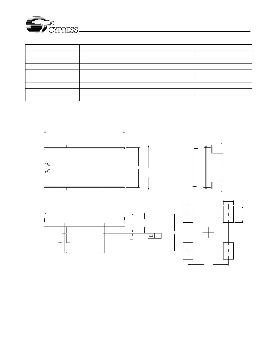
Package Drawings and Dimensions
Notes:
1. "ZZZZ" or "ZZZ" denotes the assigned product dash number. This number will be assigned by factory after the output frequency and spread percent programming
data is received from the customer.
2. "FJXC" or "FX" suffix is used for products programmed in field by Cypress distributors.
DIMENSIONS IN MILLIMETERS
5.0
(10.5 MAX)
(5.8 MAX)
10.2±0.3
5.6±0.2
0.51
5.08±0.1
0.15±0.1
2.4
2.5
(0.05 MIN)
(2.7 MAX)
+0.2
-0.1
3.6
1.0±0.2
(1.0)
1.0±0.2
(1.0)
1
4
5.08
1.3
2.1
4.6
RECOMMENDED SOLDERING PATTERN
0.1
REFERENCE JEDEC: N/A
PKG. WEIGHT: 0.24 gms
4-Lead JEC JE04A
51-85204-*A