Spread Spectrum Clock Generator
CY25818/19
Cypress Semiconductor Corporation
∑
3901 North First Street
∑
San Jose
∑
CA 95134
∑
408-943-2600
Document #: 38-07362 Rev. *A
Revised December 28, 2002
Features
∑ 8- to 32-MHz input frequency range
∑ CY25818: 8≠16 MHz
∑ CY25819: 16≠32 MHz
∑ Separate modulated and unmodulated clocks
∑ Accepts clock, crystal, and resonator inputs
∑ Down spread modulation
∑ Power-down function
∑ Low-power dissipation
-- CY25818 = 33 mW-typ @ 8 MHz
-- CY25818 = 56 mW-typ @ 16 MHz
-- CY25819 = 36 mW-typ @ 16 MHz
-- CY25819 = 63 mW-typ @ 32 MHz
∑ Low cycle-to-cycle jitter
-- SSCLK = 250 ps-typ
-- REFOUT = 275 ps-typ
∑ Available in 8-pin (150-mil) SOIC package
Applications
∑ Printers and MFPs
∑ LCD panels and notebook PCs
∑ Digital copiers
∑ PDAs
∑ Automotive
∑ CD-ROM, VCD, and DVD
∑ Networking and LAN/WAN
∑ Scanners
∑ Modems
∑ Embedded digital systems
Benefits
∑ Peak electromagnetic interference (EMI) reduction by
8≠16 dB
∑ Fast time to market
∑ Cost reduction
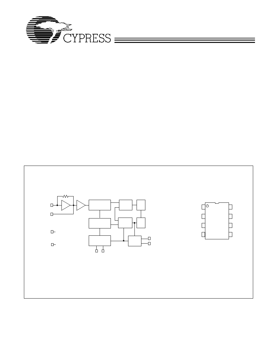
REFERENCE
DIVIDER
PD and
CP
LF
VCO
DIVIDER
and
MUX
INPUT
DECODER
1
8
300K
MODULATION
CONTROL
3
6
S0 PD#
XIN/CLKIN
XOUT
VDD
7
VSS
2
4
SSCLK
5
REFCLK
VCO
COUNTER
2
1
3
4
8
7
6
5
XIN/CLKIN
VSS
S0
SSCLK
XOUT
VDD
PD#
REFCLK
CY25818
CY25819
8 Pin SOIC
8-pin SOIC
Block Diagram
Pin Configuration
CY25818/19
Document #: 38-07362 Rev. *A
Page 2 of 8
.
Overview
The Cypress CY25818/19 products are Spread Spectrum
Clock Generator (SSCG) ICs used for the purpose of reducing
EMI found in today's high-speed digital electronic systems.
The devices use a Cypress proprietary phase-locked loop
(PLL) and Spread Spectrum Clock (SSC) technology to
synthesize and modulate the frequency of the input clock. By
frequency modulating the clock, the measured EMI at the
fundamental and harmonic frequencies is greatly reduced.
This reduction in radiated energy can significantly reduce the
cost of complying with regulatory agency requirements and
improve time to market without degrading system perfor-
mance.
The input frequency range is 8≠16 MHz for the CY25818 and
16≠32 MHz for the CY25819. Both products accept external
clock, crystal, or ceramic resonator inputs.
The CY25818/19 provide separate modulated (SSCLK) and
unmodulated reference (REFCLK) clock outputs which are the
same frequency as the input clock frequency. Down spread
frequency modulation can be selected by the user, based on
three discrete values of Spread%. A separate Power-down
function is also provided.
The CY25818/19 products are available in an 8-pin SOIC
(150-mil) package with a commercial operating temperature
range of 0≠70
∞
C. Contact Cypress for availability of ≠40 to
+85
∞
C industrial temperature range operation or TSSOP
package versions. Refer to the CY25568, CY25811,
CY25812, and CY25814 products for other functions such as
clock multiplication of 1◊, 2◊, or 4◊ to generate a wide range
of Spread Spectrum output clocks from 4 to 128 MHz.
Input Frequency Range and Selection
CY25818/19 input frequency range is 8≠32 MHz. This range
is divided into two segments, as given in Table 1.
Spread% Selection
CY25818/19 SSCG products provide Down-Spread frequency
modulation. The amount of Spread% is selected by using
3-Level S0 digital input. Spread% values are given in Table 2.
3-Level Digital Inputs
S0 digital input is designed to sense three logic levels desig-
nated as HIGH "1," LOW "0," and MIDDLE "M." With this
3-Level digital input logic, the 3-Level logic is able to detect
three different logic levels.
The S0 pin includes an on-chip 20K (10K/10K) resistor divider.
No external application resistors are needed to implement
3-Level logic, as follows.
Logic Level "0": 3-Level logic pin connected to GND.
Logic Level "M": 3-Level logic pin left floating (no connection.)
Logic Level "1": 3-Level logic pin connected to V
DD
.
Pin Description
Pin
Name
Description
1
XIN/CLK
Clock, Crystal, or Ceramic Resonator Input Pin.
2
VSS
Power Supply Ground.
3
S0
Digital Spread% Control Pin. 3-Level input (H-M-L). Default = M.
4
SSCLK
Modulated Spread Spectrum Output Clock. The output frequency is referenced to
input frequency. Refer to Table 2 for the amount of modulation (Spread%).
5
REFCLK
Unmodulated Reference Clock Output. The unmodulated output frequency is the
same as the input frequency.
6
PD#
Power-Down Control Pin. Default = H (V
DD
).
7
VDD
Positive Power Supply.
8
XOUT
Clock, Crystal, or Ceramic Resonator Output Pin. Leave this pin unconnected if an
external clock is used at X
IN
pin.
Table 1. Input and Output Frequency Selection
Product
Input/Output Frequency Range
CY25818
8≠16 MHz
CY25819
16≠32 MHz
Table 2. Spread% Selection
XIN (MHz)
Product
S0 = 1
S0 = 0
S0 = M
Down (%)
Down (%)
Down (%)
8≠10
CY25818
≠3.0
≠2.2
≠0.7
10≠12
CY25818
≠2.7
≠1.9
≠0.6
12≠14
CY25818
≠2.5
≠1.8
≠0.6
14≠16
CY25818
≠2.3
≠1.7
≠0.5
16≠20
CY25819
≠3.0
≠2.2
≠0.7
20≠24
CY25819
≠2.7
≠1.9
≠0.6
24≠28
CY25819
≠2.5
≠1.8
≠0.6
28≠32
CY25819
≠2.3
≠1.7
≠0.5
CY25818/19
Document #: 38-07362 Rev. *A
Page 3 of 8
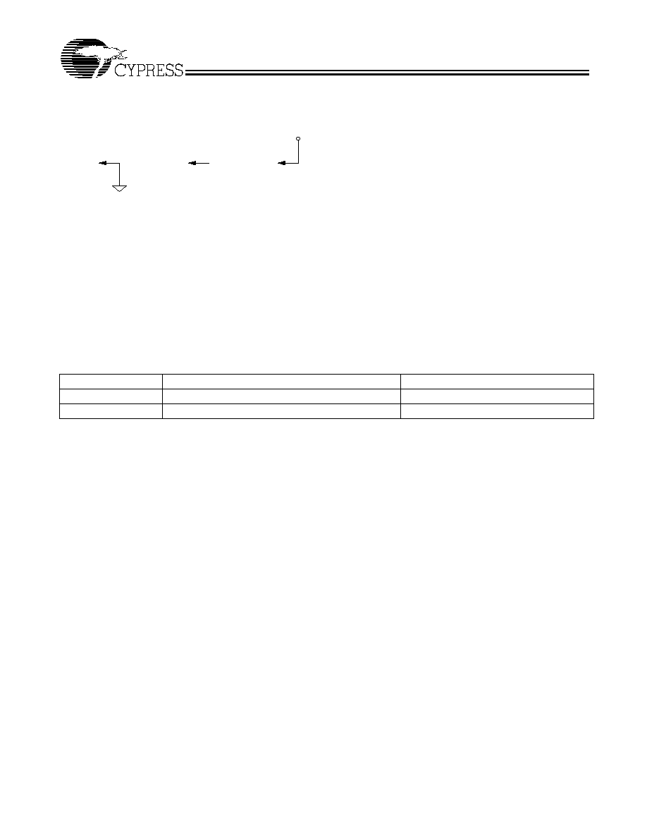
Figure 1 illustrates how to implement 3-Level Logic.
Modulation Rate
Spread Spectrum Clock Generators utilize frequency
modulation (FM) to distribute energy over a specific band of
frequencies. The maximum frequency of the clock (fmax) and
minimum frequency of the clock (fmin) determine this band of
frequencies. The time required to transition from fmin to fmax
and back to fmin is the period of the Modulation Rate, Tmod.
The Modulation Rates of SSCG clocks are generally referred
to in terms of frequency, and fmod = 1/Tmod.
The input clock frequency, fin, and the internal divider
determine the Modulation Rate.
In the case of CY25818/19 devices, the (Spread Spectrum)
Modulation Rate, fmod, is given by the following formula:
fmod = f
IN
/DR
where fmod is the Modulation Rate, f
IN
is the Input Frequency,
and DR is the Divider Ratio, as given in Table 3.
L OGI C
L OW (0 )
L OGI C
MI D D L E (M)
L OGI C
H I GH (H )
S 0
to V D D
S 0
U N CON N E CT E D
S 0
to V S S
V D D
VS S
Figure 1. 3-Level Logic
Table 3. Modulation Rate Divider Ratios
Product
Input Frequency Range
Divider Ratio (DR)
CY25818
8≠16 MHz
256
CY25819
16≠32 MHz
512
CY25818/19
Document #: 38-07362 Rev. *A
Page 4 of 8
Maximum Ratings
[1, 2]
Supply Voltage (V
DD
): ..................................................+ 5.5V
Input Voltage Relative to V
DD
: ............................. V
DD
+ 0.3V
Input Voltage Relative to V
SS
: .............................. V
SS
+ 0.3V
Operating Temperature:.................................... 0
∞
C to +70
∞
C
Storage Temperature:................................ ≠65
∞
C to + 150
∞
C
Table 4. DC Electrical Characteristics V
DD
= 3.3V ±10%, T
A
= 0∞C to +70∞C and C
L
= 15 pF (unless otherwise noted)
Parameter
Description
Conditions
Min.
Typ.
Max.
Unit
V
DD
Power Supply Range
2.97
3.3
3.63
V
V
INH
Input HIGH Voltage
S0 Input
0.85 V
DD
V
DD
V
DD
V
V
INM
Input MIDDLE Voltage
S0 Input
0.40 V
DD
0.50 V
DD
0.60 V
DD
V
V
INL
Input LOW Voltage
S0 Input
0.0
0.0
0.15 V
DD
V
V
OH1
Output HIGH Voltage
I
OH
= 4 ma, SSCLK and REFCLK
2.4
V
V
OH2
Output HIGH Voltage
I
OH
= 6 ma, SSCLK and REFCLK
2.0
V
V
OL1
Output LOW Voltage
I
OL
= 4 ma, SSCLK Output
0.4
V
V
OL2
Output LOW Voltage
I
OL
= 10 ma, SSCLK Output
1.2
V
C
IN1
Input Capacitance
X
IN
(Pin 1) and X
OUT
(Pin 8)
6.0
7.5
9.0
pF
C
IN2
Input Capacitance
All Digital Inputs
3.5
4.5
6.0
pF
I
DD1
Power Supply Current
F
IN
=8 MHz, no load
10.0
12.5
mA
I
DD3
Power Supply Current
F
IN
=32 MHz, no load
19.0
23.0
mA
I
DD4
Power Supply Current
PD#=V
SS
150
250
µ
A
Table 5. Timing Electrical Characteristics V
DD
= 3.3V ±10%, T
A
= 0∞C to +70∞C and C
L
= 15 pF (unless otherwise noted)
Parameter
Description
Conditions
Min.
Typ.
Max.
Unit
ICLKFR1
Input Frequency Range
CY25818
8
16
MHz
ICLKFR2
Input Frequency Range
CY25819
16
32
MHz
trise1
Clock Rise Time
SSCLK and REFCLK, 0.4V to 2.4V
2.0
3.0
4.0
ns
tfall1
Clock Fall Time
SSCLK and REFCLK, 0.4V to 2.4V
2.0
3.0
4.0
ns
CDCin
Input Clock Duty Cycle
X
IN
20
50
80
%
CDCout
Output Clock Duty Cycle
SSCLK and REFCLK @ 1.5V
45
50
55
%
CCJss
Cycle-to-Cycle Jitter
SSCLK; F
IN
= F
OUT
= 8≠32 MHz
250
350
ps
CCJref
Cycle-to-Cycle Jitter
REFCLK; F
IN
= F
OUT
= 8≠32 MHz
275
375
ps
Ordering Information
Part Number
Package Type
Product Flow
CY25818SC
8-pin SOIC
Commercial, 0
∞
to 70
∞
C
CY25818SCT
8-pin SOIC ≠ Tape and Reel
Commercial, 0
∞
to 70
∞
C
CY25819SC
8-pin SOIC
Commercial, 0
∞
to 70
∞
C
CY25819SCT
8-pin SOIC ≠ Tape and Reel
Commercial, 0
∞
to 70
∞
C
Note:
1.
Single Power Supply: The voltage on any input or I/O pin cannot exceed the power pin during power-up.
2.
Operation at any Absolute Maximum Rating is not implied.
CY25818/19
Document #: 38-07362 Rev. *A
Page 5 of 8
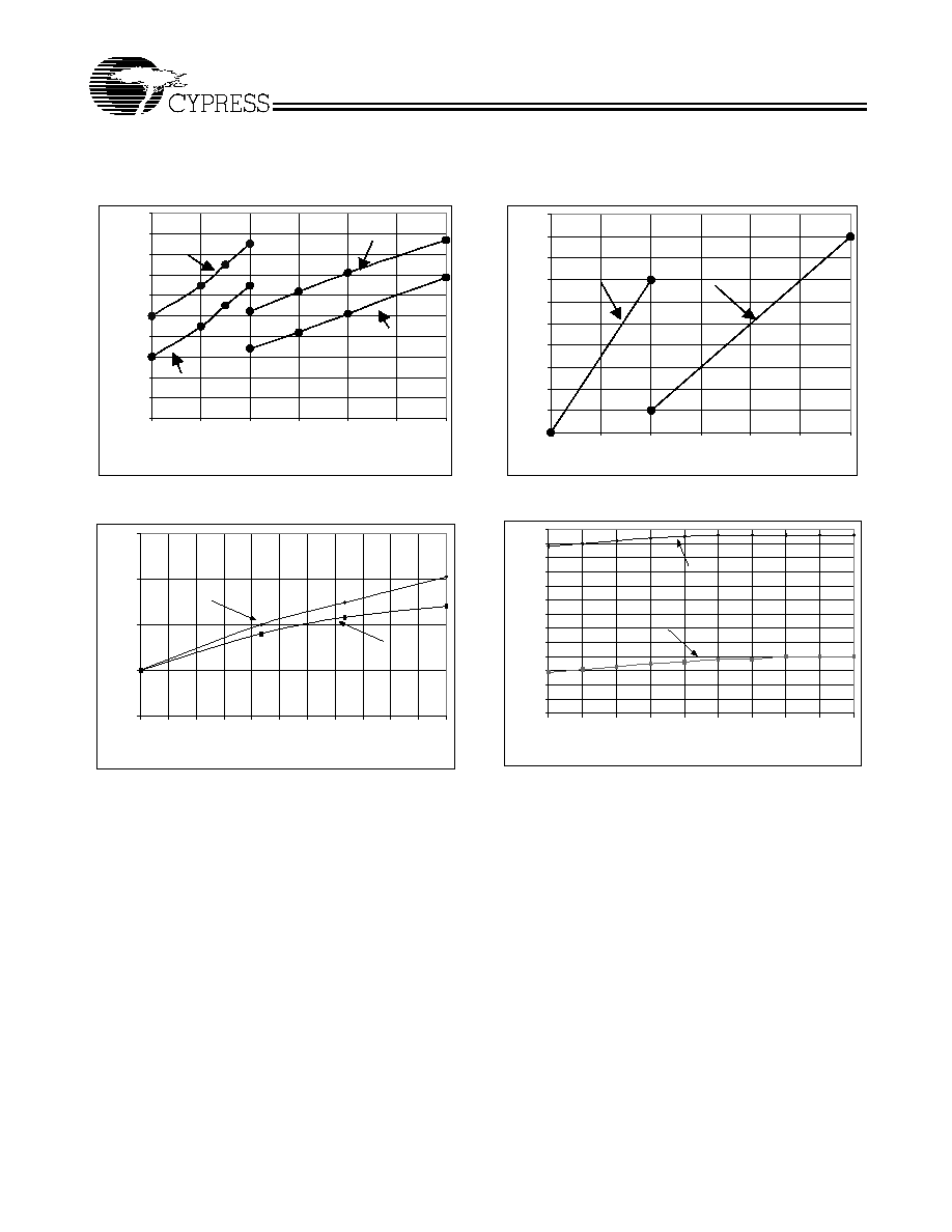
Characteristics Curves
The following curves demonstrate the characteristic behavior
of the CY25818/19 when tested over a number of environ-
mental and application specific parameters. These are typical
performance curves and are not meant to replace any
parameter specified in Table 4 and Table 5.
2 0 0
2 1 0
2 2 0
2 3 0
2 4 0
2 5 0
2 6 0
2 7 0
2 8 0
2 9 0
3 0 0
8
1 2
1 6
2 0
2 4
2 8
3 2
F r equ en cy ( MH z )
CCJ
(p
s
)
R E F CL K CY 2 5 8 18
S S CL K CY2 5 8 18
R E F CL K CY 2 5 8 19
S S CL K CY2 5 8 19
Figure 2. CCJ (ps) vs. Frequency (MHz)
1.75
2
2.25
2.5
2.75
-40
-25
-10
5
20
35
50
65
80
95
110
125
Temp (C)
BW
%
12 MHz
32.0 MHz
Figure 3. Bandwidth% vs. Temperature
10
11
12
13
14
15
16
17
18
19
2 0
8
12
16
2 0
2 4
2 8
3 2
F r equ en cy ( MH z )
I
DD(m
A
)
C Y 2 5 8 19
16 - 3 2 M H z
C Y 2 5 8 18
8 - 16 M H z
Figure 4. IDD (mA) vs. Frequency (MHz)
1.8
1.9
2
2.1
2.2
2.3
2.4
2.5
2.6
2.7
2.8
2.9
3
3.1
2.8
2.9
3
3.1
3.2
3.3
3.4
3.5
3.6
3.7
VDD (volts)
BW
(
%
)
CY25819@32 MHz
CY25818@8.0 MHz
Figure 5. Bandwidth% vs. V
DD
CY25818/19
Document #: 38-07362 Rev. *A
Page 6 of 8
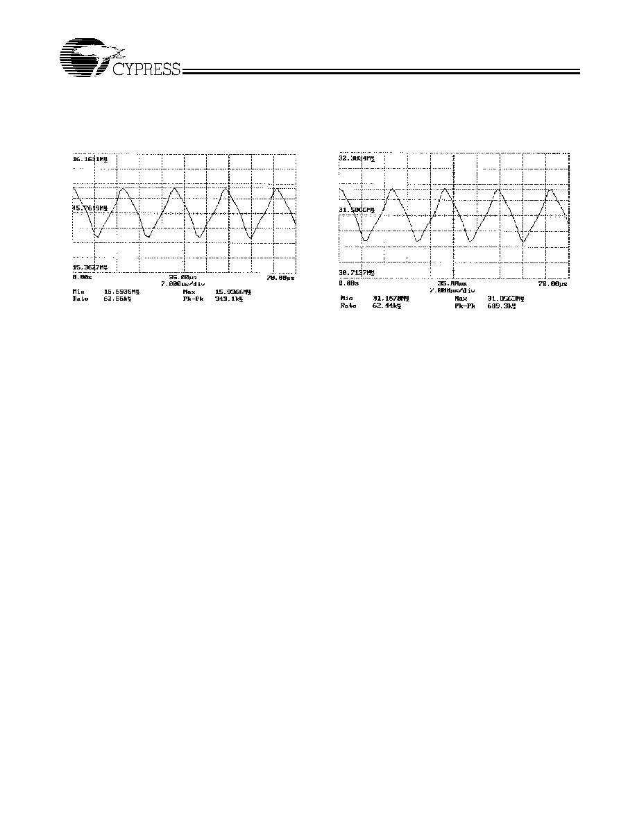
SSCG Profiles
CY25818/19 SSCG products use a non-linear "optimized"
frequency profile as shown in Figure 6 and Figure 7. The use
of Cypress proprietary "optimized" frequency profile maintains
flat energy distribution over the fundamental and higher order
harmonics. This results in additional EMI reduction in
electronic systems.
Notes:
1.
X
IN
= 16.0 MHz; S0 = 1; SSCLK = 16.0 MHz; BW = ≠2.14%.
2.
Xin = 32.0MHz; S0 = 1; SSCLK = 32.0 MHz; BW = -2.15%
Figure 6. CY25818 Spread Spectrum Profile
(Frequency vs. Time)
[1]
Figure 7. CY25819 Spread Spectrum Profile
(Frequency vs. Time)
[2]
CY25818/19
Document #: 38-07362 Rev. *A
Page 7 of 8
© Cypress Semiconductor Corporation, 2002. The information contained herein is subject to change without notice. Cypress Semiconductor Corporation assumes no responsibility for the use
of any circuitry other than circuitry embodied in a Cypress Semiconductor product. Nor does it convey or imply any license under patent or other rights. Cypress Semiconductor does not authorize
its products for use as critical components in life-support systems where a malfunction or failure may reasonably be expected to result in significant injury to the user. The inclusion of Cypress
Semiconductor products in life-support systems application implies that the manufacturer assumes all risk of such use and in doing so indemnifies Cypress Semiconductor against all charges.
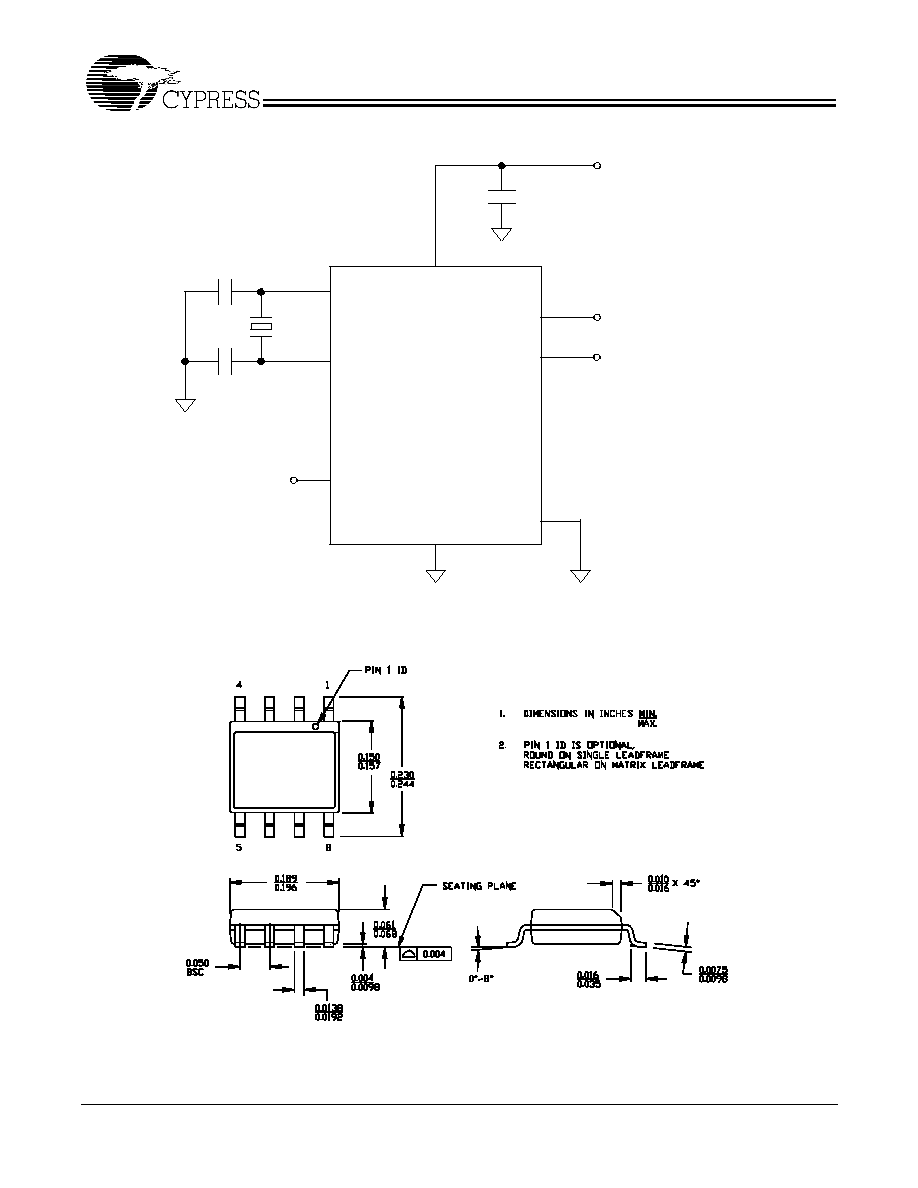
Application Schematic
Package Drawing and Dimensions
All product and company names mentioned in this document may be the trademarks of their respective holders.
VDD
1
8
14.3 MHz
or
27.0 MHz
VSS
S0
XIN
XOUT
SSCLK
VDD
CY25818
CY25819
3
4
0.1 uF
C3
C2
C3
27 pF
27 pF
14.3 MHz (CY25818)
27.0 MHz (CY25819)
REFCLK
5
2
7
PD#
6
Figure 8. Typical Application Schematic
8-lead (150-mil) SOIC S8
51-85066-A

CY25818/19
Document #: 38-07362 Rev. *A
Page 8 of 8
Document Title: CY25818/19 Spread Spectrum Clock Generator
Document Number: 38-07362
REV.
ECN NO.
Issue
Date
Orig. of
Change
Description of Change
**
112462
03/21/02
OXC
New Data Sheet
*A
122701
12/28/02
RBI
Added power up requirements to maximum rating information.