 | –≠–ª–µ–∫—Ç—Ä–æ–Ω–Ω—ã–π –∫–æ–º–ø–æ–Ω–µ–Ω—Ç: CY25822-2 | –°–∫–∞—á–∞—Ç—å:  PDF PDF  ZIP ZIP |
CK-SSC Spread Spectrum Clock Generator
CY25822-2
Cypress Semiconductor Corporation
∑
3901 North First Street
∑
San Jose
,
CA 95134
∑
408-943-2600
Document #: 38-07531 Rev. **
Revised March 18, 2003
Features
∑ 3.3V operation
∑ 48- and 66-MHz frequency support
∑ Selectable slew rate control
∑ 350-pS jitter
∑ I
2
C programmability
∑ 500-
µ
A power-down current
∑ Spread Spectrum for best electromagnetic interference
(EMI) reduction
∑ 8-pin SOIC package
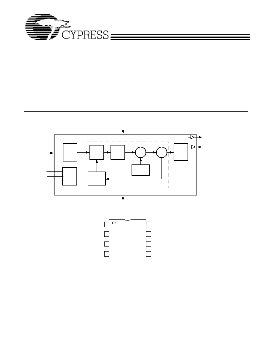
Block Diagram
Pin Configuration
1
2
3
4
8
7
6
5
C L K IN
V D D
G N D
* P W R D W N #
S C L O C K
S D A T A
R E F O U T
C Y 2 5 8 2 2 - 2
C L K O U T
* 1 5 0 K
P u ll-u p
Freq.
Phase
Modulating
VCO
Post
CLKOUT
Detector
Charge
Pump
Waveform
Dividers
Divider
Feedback
Divider
PLL
GND
VDD
M
N
Clock Input
(SSCG Output)
REFOUT
Logic
Control
SDATA
SCLOCK
PWRDWN#
CY25822-2
Document #: 38-07531 Rev. **
Page 2 of 9
Serial Data Interface
To enhance the flexibility and function of the clock synthesizer,
a two-signal serial interface is provided. Through the Serial
Data Interface, various device functions such as individual
clock output buffers, etc., can be individually enabled or
disabled.
The registers associated with the Serial Data Interface
initializes to their default setting upon power-up, and therefore
use of this interface is optional. Clock device register changes
are normally made upon system initialization, if any are
required. The interface can also be used during system
operation for power management functions.
Data Protocol
The clock driver serial protocol accepts byte write, byte read,
block write, and block read operation from the controller. For
block write/read operation, the bytes must be accessed in
sequential order from lowest to highest byte (most significant
bit first) with the ability to stop after any complete byte has
been transferred. For byte write and byte read operations, the
system controller can access individual indexed bytes. The
offset of the indexed byte is encoded in the command code, as
described in Table 1.
The block write and block read protocol is outlined in Table 2
while Table 3 outlines the corresponding byte write and byte
read protocol.The slave receiver address is 11010100 (D4h).
Pin Description
Pin No.
Pin Name
Pin Type
Pin Description
1
CLKIN
Input
48-MHz or 66-MHz Clock Input.
2
VDD
Power
Power Supply for PLL and Outputs.
3
GND
Ground
Ground for Outputs.
4
CLKOUT
Output
48-MHz or 66-MHz Spread Spectrum Clock Output.
5
REFOUT
Output
Non-spread Spectrum Reference Clock Output.
6
SDATA
I/O
I
2
C-compatible SDATA.
7
SCLOCK
Input
I
2
C-compatible SCLOCK.
8
PWRDWN#
Output
LVTTL Input for PowerDown# Active Low.
Table 1. Command Code Definition
Bit
Description
7
0 = Block read or block write operation
1 = Byte read or byte write operation
(6:0) Byte offset for byte read or byte write operation. For block read or block write operations, these bits should be '0000000'
Table 2. Block Read and Block Write Protocol
Block Write Protocol
Block Read Protocol
Bit
Description
Bit
Description
1
Start
1
Start
2:8
Slave address ≠ 7 bits
2:8
Slave address ≠ 7 bits
9
Write = 0
9
Write = 0
10
Acknowledge from slave
10
Acknowledge from slave
11:18
Command Code ≠ 8 bits
'00000000' stands for block operation
11:18
Command Code ≠ 8 bits
'00000000' stands for block operation
19
Acknowledge from slave
19
Acknowledge from slave
20:27
Byte Count ≠ 8 bits
20
Repeat start
28
Acknowledge from slave
21:27
Slave address ≠ 7 bits
29:36
Data byte 1 ≠ 8 bits
28
Read = 1
37
Acknowledge from slave
29
Acknowledge from slave
38:45
Data byte 2 ≠ 8 bits
30:37
Byte count from slave ≠ 8 bits
46
Acknowledge from slave
38
Acknowledge
....
......................
39:46
Data byte from slave ≠ 8 bits
....
Data Byte (N≠1) ≠8 bits
47
Acknowledge
....
Acknowledge from slave
48:55
Data byte from slave ≠ 8 bits
CY25822-2
Document #: 38-07531 Rev. **
Page 3 of 9
....
Data Byte N ≠8 bits
56
Acknowledge
....
Acknowledge from slave
....
Data bytes from slave/Acknowledge
....
Stop
....
Data byte N from slave ≠ 8 bits
....
Not Acknowledge
....
Stop
Table 2. Block Read and Block Write Protocol (continued)
Table 3. Byte Read and Byte Write Protocol
Byte Write Protocol
Byte Read Protocol
Bit
Description
Bit
Description
1
Start
1
Start
2:8
Slave address ≠ 7 bits
2:8
Slave address ≠ 7 bits
9
Write = 0
9
Write = 0
10
Acknowledge from slave
10
Acknowledge from slave
11:18
Command Code ≠ 8 bits
'1xxxxxxx' stands for byte operation, bits[6:0] of
the command code represents the offset of the
byte to be accessed
11:18
Command Code ≠ 8 bits
'1xxxxxxx' stands for byte operation, bits[6:0]
of the command code represents the offset of
the byte to be accessed
19
Acknowledge from slave
19
Acknowledge from slave
20:27
Data byte from master ≠ 8 bits
20
Repeat start
28
Acknowledge from slave
21:27
Slave address ≠ 7 bits
29
Stop
28
Read = 1
29
Acknowledge from slave
30:37
Data byte from slave ≠ 8 bits
38
Not Acknowledge
39
Stop
Byte 0: Control Register
Bit
@Pup
Pin#
Name
Pin Description
7
1
4
SS0
≠
6
0
4
SS1
≠
5
0
4
SS2
≠
4
0
4
SS3
≠
3
1
Not Applicable
Reserved, must be written as 1
2
1
4, 5
CLKOUT,
REFOUT
Power-down three-state enable
0 = three-state outputs, 1 = drive outputs low
(Applies only in Power Down State)
1
1
4
CLKOUT
Spread Spectrum enable
0 = spread off, 1 = spread on
0
0
Not Applicable
No Pins
Table 4. Spread Spectrum Select
SS3
SS2
SS1
SS0
Spread Mode
Spread Amount%
0
0
0
0
Down
0.8
0
0
0
1
Down
1.0
0
0
1
0
Down
1.25
0
0
1
1
Down
1.5
0
1
0
0
Down
1.75
CY25822-2
Document #: 38-07531 Rev. **
Page 4 of 9
Bytes 2 through 5: Reserved Registers
PWRDWN# (Power-down) Clarification
The PWRDWN# (Power-down) pin is used to shut off ALL
clocks prior to shutting off power to the device. PWRDWN# is
an asynchronous active LOW input. This signal is synchro-
nized internally to the device powering down the clock synthe-
sizer. PWRDWN# is an asynchronous function for powering up
the system. When PWRDWN# is low, all clocks are driven to
a LOW value and held there and the VCO and PLLs are also
powered down. All clocks are shut down in a synchronous
manner so has not to cause glitches while transitioning to the
low `stopped' state. When PWRDWN# is deasserted the
clocks should remain stopped until the VCO is stable and
within specification (t
STABLE
). A stopped clock is either
tri-stated or driven low depending on the state of the tri-state
enable I
2
C register bit. CY25822 clocks that are stopped in the
driven state are driven low.
The CLKIN input must be on and within specified operating
parameters before PWRDWN# is asserted and it must remain
in this state while PWRDWN# is asserted.
0
1
0
1
Down
2.0
0
1
1
0
Down
2.5
0
1
1
1
Down
3.0
1
0
0
0
Center
±0.3
1
0
0
1
Center
±0.4
1
0
1
0
Center
±0.5
1
0
1
1
Center
±0.6
1
1
0
0
Center
±0.8
1
1
0
1
Center
±1.0
1
1
1
0
Center
±1.25
1
1
1
1
Center
±1.5
Table 4. Spread Spectrum Select (continued)
SS3
SS2
SS1
SS0
Spread Mode
Spread Amount%
Byte 1: Control Register
Bit
@Pup
Pin#
Name
Pin Description
7
1
5
REFEN
REFOUT enable
0 = disabled, 1 = enabled
6
1
5
REFSLEW
REFOUT edge rate control
0 = slow, 1 = nominal
5
0
Not Applicable
Reserved.
4
0
Not Applicable
Reserved
3
1
4
CLKSLEW
CLKOUT edge rate control
0 = slow, 1 = nominal
2
1
4
CLKEN
CLKOUT enable
0 =disabled, 1 = enabled
1
0
Not Applicable
Reserved
0
0
Not Applicable
Reserved
Byte 6: Vendor/Revision ID Register
Bit
@Pup
Pin#
Name
Pin Description
7
0
≠
≠
Revision ID Bit 3
6
0
≠
≠
Revision ID Bit 2
5
0
≠
≠
Revision ID Bit 1
4
0
≠
≠
Revision ID Bit 0
3
1
≠
≠
Vendor ID Bit 3
2
0
≠
≠
Vendor ID Bit 2
1
0
≠
≠
Vendor ID Bit 1
0
0
≠
≠
Vendor ID Bit 0
CY25822-2
Document #: 38-07531 Rev. **
Page 5 of 9
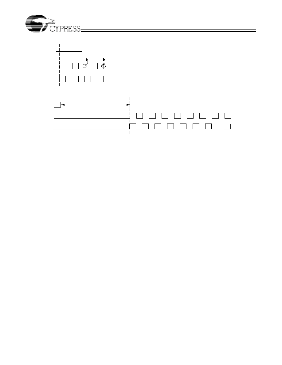
CLKOUT and REFOUT Enable Clarification
The CLKOUT enable and REFOUT enable I
2
C register bits are
used to shot-off the CLKOUT and REFOUT clocks individually.
The VCO and crystal oscillator must remain on. A shutdown
clock is driven low. ALL clocks need to be stopped in a
predictable manner. All clocks need to be shutdown without
any glitches or other abnormal behavior while transitioning to
a stopped state. Similarly when CLKOUT or REFOUT is
enabled the clock must start in a predictable manner without
any glitches or abnormal behavior.
REFOUT
PWRDWN#
CLKOUT
Figure 1. Power-down Assertion
P D #
C LK O U T
R E F O U T
< 3.0 m s
Figure 2. Power-down Deassertion
CY25822-2
Document #: 38-07531 Rev. **
Page 6 of 9
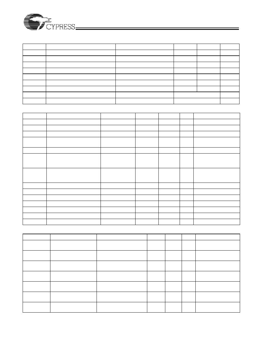
Table 5. Absolute Maximum Ratings
Parameter
Description
Condition
Min.
Max.
Unit
V
DD
Core Supply Voltage
≠0.5
4.6
V
V
DD_A
Analog Supply Voltage
≠0.5
4.6
V
V
IN
Input Voltage
Relative to V
SS
≠0.5
V
DD
+ 0.5
VDC
T
S
Temperature, Storage
Non Functional
≠65
+150
∞C
T
A
Temperature, Operating Ambient
Functional
0
70
∞C
T
J
Temperature, Junction
Functional
≠
150
∞C
ESD
HBM
ESD Protection (Human Body Model)
MIL-STD-883, Method 3015
2000
≠
Volts
UL≠94
Flammability Rating
@1/8 in.
V≠0
MSL
Moisture Sensitivity Level
1
Table 6. DC Parameters (T
A
= 0∞C to +70∞C, V
DD
= 3.3V ± 5%)
Parameter
Description
Condition
Min.
Max
Unit
Notes
V
DD
Supply Voltage
≠
3.135
3.465
V
V
DD
= 3.3 ± 5%
V
IH
Input High Voltage
≠
2.0
V
DD
+ 0.3
V
V
IL
Input Low Voltage
≠
V
SS
≠ 0.3
0.8
V
I
IL1
Input Leakage Current
SCLOCK
or SDATA
≠25
+25
µ
A
I
IL2
Input Leakage Current
PWRDWN#
≠75
≠15
µ
A
V
OH
Output High Voltage
I
OH
= ≠4 mA
2.4
≠
V
Single edge is required to
be monotonic when transi-
tioning through this region.
V
OL
Output Low Voltage
I
OL
= 4 mA
≠
0.4
V
Single edge is required to
be monotonic when transi-
tioning through this region.
C
IN
Input Pin Capacitance
≠
≠
5
pF
C
OUT
Output Pin Capacitance
≠
≠
6
pF
L
IN
Pin Inductance
≠
≠
7
nH
T
A
Ambient Temperature
≠
0
70
∞C
No air flow
I
DD1
Supply Current
@ 66 MHz
≠
50
mA
I
DD2
Supply Current
@ 48 MHz
≠
40
mA
I
PD
Power Down Supply Current
≠
≠
500
µ
A
Table 7. AC Parameters (T
A
= 0∞C to +70∞C, V
DD
= 3.3V ± 5%)
Parameter
Description
Conditions
Min.
Max.
Unit
Notes
t
HIGH
CLK High Time, 48MHz
Measured @2.4V
9.45
10.95
ns
Specification applies to
48MHz output mode.
t
LOW
CLK, Low Time, 48MHz
Measured @0.4V
8.50
10.10
ns
Specification applies to
48MHz output mode.
t
HIGH
CLK High Time, 66MHz
Measured @2.4V
6.85
7.90
ns
Specification applies to
66.7MHz output mode.
t
LOW
CLK Low Time, 66MHz
Measured @0.4V
5.95
6.95
ns
Specification applies to
66.7MHz output mode.
t
RISEH1
Rising Edge Rate
Measured from 0.4V to 2.4V
REFOUT and CLOCKOUT
2.0
5.0
V/ns
High Buffer Strength
Refer to I
2
C Control
t
FALLH1
Falling Edge Rate
Measured from 2.4V to 0.4V
REFOUT and CLOCKOUT
2.0
5.0
V/ns
High Buffer Strength
Refer to I
2
C Control
t
RISEL1
Rising Edge Rate
Measured from 0.4V to 2.4V
REFOUT and CLOCKOUT
1.33
4.0
V/ns
Low Buffer Strength
Refer to I
2
C Control
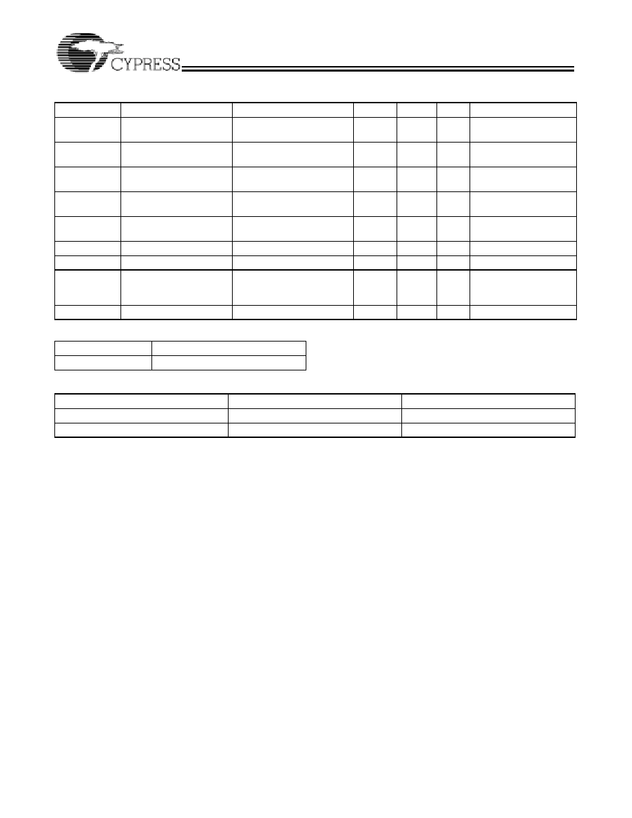
CY25822-2
Document #: 38-07531 Rev. **
Page 7 of 9
t
FALLL1
Falling Edge Rate
Measured from 2.4V to 0.4V
REFOUT and CLOCKOUT
1.33
4.0
V/ns
Low Buffer Strength
Refer to I
2
C Control
t
RISEH2
Rise Time
Measured from 0.4V to 2.4V
REFOUT and CLOCKOUT
0.4
1.0
ns
High Buffer Strength
Refer to I
2
C Control
t
FALLH2
Fall Time
Measured from 2.4V to 0.4V
REFOUT and CLOCKOUT
0.4
1.0
ns
High Buffer Strength
Refer to I
2
C Control
t
RISEL2
Rise Time
Measured from 0.4V to 2.4V
REFOUT and CLOCKOUT
0.5
1.5
ns
Low Buffer Strength
Refer to I
2
C Control
t
FALLL2
Fall Time
Measured from 2.4V to 0.4V
REFOUT and CLOCKOUT
0.5
1.5
ns
Low Buffer Strength
Refer to I
2
C Control
T
CYC1
Cycle to Cycle Jitter
REFOUT
≠
500
ps
SSCG is ON
T
CYC2
Cycle to Cycle Jitter
CLOCKOUT
≠
250
ps
SSCG is ON
LTJ
10
µ
S Period Jitter
(100KHz, Frequency Mod-
ulation Amplitude)
Applies to REFOUT at all
times and CLOCKOUT when
SSCG is Off
≠
2.0
ns
≠
t
START
Start up time
From VDD = 2.0 V
≠
3.0
ms
All outputs disabled
Table 7. AC Parameters (T
A
= 0∞C to +70∞C, V
DD
= 3.3V ± 5%) (continued)
Parameter
Description
Conditions
Min.
Max.
Unit
Notes
Table 8. Signal Loading Table
Clock Name
Max Load (pF)
CLKOUT, REFOUT
15
Ordering Information
Part Number
Package Type
Product Flow
CY25822SC≠2
8-pin SOIC
Commercial, 0∞C to 70∞C
CY25822SC≠2T
8-pin SOIC ≠ Tape and Reel
Commercial, 0∞C to 70∞C
CY25822-2
Document #: 38-07531 Rev. **
Page 8 of 9
© Cypress Semiconductor Corporation, 2003. The information contained herein is subject to change without notice. Cypress Semiconductor Corporation assumes no responsibility for the use
of any circuitry other than circuitry embodied in a Cypress Semiconductor product. Nor does it convey or imply any license under patent or other rights. Cypress Semiconductor does not authorize
its products for use as critical components in life-support systems where a malfunction or failure may reasonably be expected to result in significant injury to the user. The inclusion of Cypress
Semiconductor products in life-support systems application implies that the manufacturer assumes all risk of such use and in doing so indemnifies Cypress Semiconductor against all charges.
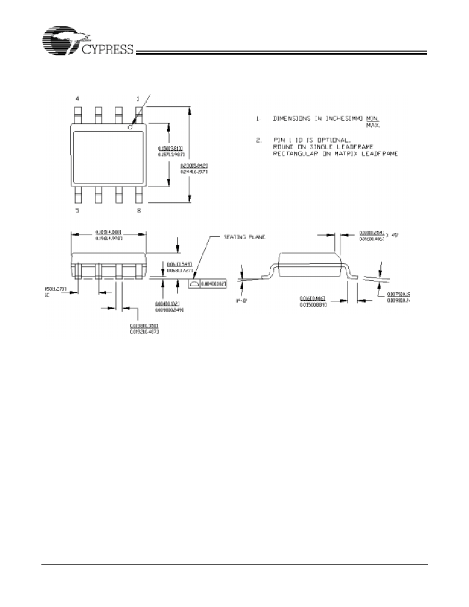
Package Diagram
Purchase of I
2
C components from Cypress, or one of its sublicensed Associated Companies, conveys a license under the Philips
I
2
C Patent Rights to use these components in an I
2
C system, provided that the system conforms to the I
2
C Standard Specification
as defined by Philips.All product and company names mentioned in this document are trademarks of their respective holders.
8-lead (150-Mil) SOIC ≠ S8
51-85066-*B

CY25822-2
Document #: 38-07531 Rev. **
Page 9 of 9
Document History Page
Document Title: CY25822-2 CK-SSC Spread Spectrum Clock Generator
Document Number: 38-07531
REV.
ECN NO.
Issue
Date
Orig. of
Change
Description of Change
**
124462
03/19/03
RGL
New Data Sheet