CK-SSCD Spread Spectrum Differential Clock
Specification
CY25823
Cypress Semiconductor Corporation
∑
3901 North First Street
∑
San Jose
,
CA 95134
∑
408-943-2600
Document #: 38-07579 Rev. *C
Revised September 02, 2004
Features
∑ 3.3V operation
∑ 96- and 100-MHz frequency support
∑ Selectable slew rate control
∑ 200-ps jitter
∑ I
2
C programmability
∑ 250-
µA power-down current
∑ Lexmark Spread Spectrum for best electromagnetic
interference (EMI) reduction
∑ 16-pin TSSOP package
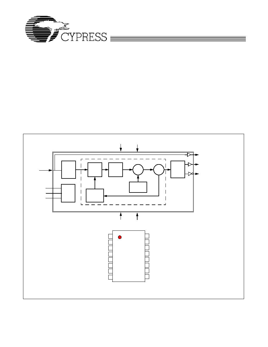
Block Diagram
Pin Configuration
Freq.
Phase
Modulating
VCO
Post
CLKOUT
Detector
Charge
Pump
Waveform
Dividers
Divider
Feedback
Divider
PLL
VSS
VDD
M
N
Clock Input
(SSCG Output)
REFOUT
Logic
Control
SDATA
SCLK
PWRDWN
16 pin TSSOP
1
2
3
4
5
6
7
8
16
15
14
13
12
11
10
9
VDDA
VSSA
IREF
VSSIREF
CLKOUT
CLKOUT#
VSS
VDD
CLKIN
S3
S2
S1
PW RDW N
REFOUT/SEL
SCLK
SDATA
VDDA
CLKOUT#
VSSA
CY25823
Document #: 38-07579 Rev. *C
Page 2 of 12
Serial Data Interface
To enhance the flexibility and function of the clock synthesizer,
a two-signal serial interface is provided. Through the Serial
Data Interface, various device functions such as individual
clock output buffers can be individually enabled or disabled.
The registers associated with the Serial Data Interface
initializes to their default setting upon power-up, and therefore
use of this interface is optional. Clock device register changes
are normally made upon system initialization, if any are
required. The interface can also be used during system
operation for power management functions.
Data Protocol
The clock driver serial protocol accepts byte write, byte read,
block write, and block read operation from the controller. For
block write/read operation, the bytes must be accessed in
sequential order from lowest to highest byte (most significant
bit first) with the ability to stop after any complete byte has
been transferred. For byte write and byte read operations, the
system controller can access individual indexed bytes. The
offset of the indexed byte is encoded in the command code,
as described in Table 1.
The block write and block read protocol is outlined in Table 2
while Table 3 outlines the corresponding byte write and byte
read protocol.The combined 7 bits slave address and
read/write bit form a complete block write (D4h) or block read
(D5h) command.
Pin Definitions
Pin No.
Name
Type
Description
1
CLKIN
Input
3.3V 14.131818-MHz single-ended clock input
2,3,4
S[3:1]
Input
Spread Spectrum configuration
5
PWRDWN
Input
3.3V LVTTL input for power-down active high, no pull-up or pull-down
6
REFOUT/SEL
I/O
Latched input during power-up, 1 (10K external pull-up) = 100 MHz or 0
(10K external pull-down) = 96 MHz. After power-up it becomes 14.31818-MHz
REFOUT clock.
7
SCLK
Input
SMBus-compatible SCLK
8
SDATA
I/O
SMBus-compatible SDATA
9
VDD
3.3V
3.3V power supply for logic and outputs
10
VSS
Ground
Ground for logic and outputs
11
CLKOUT#
Output
0.7V 96-MHz or 100-MHz Spread Spectrum differential clock output
12
CLKOUT
Output
0.7V 96-MHz or 100-MHz Spread Spectrum differential clock output
13
VSSIREF
Ground
Current reference ground
14
IREF
Input
Typically a precision 475
external resistor is connected between this
pin and VSSIREF to set IOUT (drive current) of CLKOUT differential
driver.
15
VSSA
Ground
Ground for PLL
16
VDDA
3.3V
3.3V power supply for PLL
Table 1. Command Code Definition
Bit
Description
7
0 = Block read or block write operation
1 = Byte read or byte write operation
(6:0)
Byte offset for byte read or byte write operation. For block read or block write operations, these bits should
be '0000000'
Table 2. Block Read and Block Write Protocol
Block Write Protocol
Block Read Protocol
Bit
Description
Bit
Description
1
Start
1
Start
2:8
Slave address ≠ 7 bits (D4)
2:8
Slave address ≠ 7 bits (D5)
9
Write = 0
9
Read = 0
10
Acknowledge from slave
10
Acknowledge from slave

CY25823
Document #: 38-07579 Rev. *C
Page 3 of 12
11:18
Command Code ≠ 8 bits
'00000000' stands for block operation
11:18
Command Code ≠ 8 bits
'00000000' stands for block operation
19
Acknowledge from slave
19
Acknowledge from slave
20:27
Byte Count ≠ 8 bits
20
Repeat start
28
Acknowledge from slave
21:27
Slave address ≠ 7 bits
29:36
Data byte 0 ≠ 8 bits
28
Read = 1
37
Acknowledge from slave
29
Acknowledge from slave
38:45
Data byte 1 ≠ 8 bits
30:37
Byte count from slave ≠ 8 bits
46
Acknowledge from slave
38
Acknowledge
....
......................
39:46
Data byte from slave ≠ 8 bits
....
Data Byte (N≠1) ≠8 bits
47
Acknowledge
....
Acknowledge from slave
48:55
Data byte from slave ≠ 8 bits
....
Data Byte N ≠8 bits
56
Acknowledge
....
Acknowledge from slave
....
Data bytes from slave/Acknowledge
....
Stop
....
Data byte N from slave ≠ 8 bits
....
Not Acknowledge
....
Stop
Table 3. Byte Read and Byte Write Protocol
Byte Write Protocol
Byte Read Protocol
Bit
Description
Bit
Description
1
Start
1
Start
2:8
Slave address ≠ 7 bits (D4)
2:8
Slave address ≠ 7 bits (D5)
9
Write = 1
9
Read = 1
10
Acknowledge from slave
10
Acknowledge from slave
11:18
Command Code ≠ 8 bits
'100000xx' stands for byte operation, bits[1:0] of
the command code represents the offset of the
byte to be accessed
11:18
Command Code ≠ 8 bits
'100000xx' stands for byte operation, bits[1:0]
of the command code represents the offset of
the byte to be accessed
19
Acknowledge from slave
19
Acknowledge from slave
20:27
Data byte from master ≠ 8 bits
20
Repeat start
28
Acknowledge from slave
21:27
Slave address ≠ 7 bits
29
Stop
28
Read = 1
29
Acknowledge from slave
30:37
Data byte from slave ≠ 8 bits
38
Not Acknowledge
39
Stop
Byte 0: Control Register
Bit
@Power-up
Pin#
Name
Pin Description
7
0
11, 12
SS0
≠
6
S1
11, 12
SS1
≠
5
S2
11, 12
SS2
≠
4
S3
11, 12
SS3
≠
3
SEL100/96#
6
SEL100/96#
Select output frequency, 1 = 100 MHz, 0 = 96 MHz
Table 2. Block Read and Block Write Protocol (continued)
Block Write Protocol
Block Read Protocol
Bit
Description
Bit
Description
CY25823
Document #: 38-07579 Rev. *C
Page 4 of 12
2
0
Reserved must equal 0
1
1
11, 12
Spread Enable
Spread spectrum enable, 0 = Disable, 1 = Enable
0
0
HW/SW Control
Hardware/software control of S[3:0], and output frequency.
0 = hardware control, 1= software control.
Table 4. Spread Spectrum Select (Charge Pump = 00 or Default Condition)
SS3
SS2
SS1
SS0
Spread Mode
Spread Amount %
0
0
0
0
Down
0.65
0
0
0
1
Down
0.80
0
0
1
0
Down
0.90
0
0
1
1
Down
1.10
0
1
0
0
Down
1.30
0
1
0
1
Down
1.40
0
1
1
0
Down
1.80
0
1
1
1
Down
2.25
1
0
0
0
Center
±0.25
1
0
0
1
Center
±0.30
1
0
1
0
Center
±0.40
1
0
1
1
Center
±0.45
1
1
0
0
Center
±0.60
1
1
0
1
Center
±0.80
1
1
1
0
Center
±1.00
1
1
1
1
Center
±1.10
Table 5. Spread Spectrum Select (Charge Pump = 11 and 01)
SS3
SS2
SS1
SS0
Spread Mode
Spread Amount %
(Charge pump = 11)
Spread Amount %
(Charge pump = 01)
0
0
0
0
Down
0.80
0.90
0
0
0
1
Down
0.90
1.10
0
0
1
0
Down
1.20
1.40
0
0
1
1
Down
1.40
1.60
0
1
0
0
Down
1.60
2.00
0
1
0
1
Down
1.75
2.20
0
1
1
0
Down
2.20
2.75
0
1
1
1
Down
2.60
3.30
1
0
0
0
Center
±0.38
±0.40
1
0
0
1
Center
±0.40
±0.50
1
0
1
0
Center
±0.50
±0.60
1
0
1
1
Center
±0.60
±0.70
1
1
0
0
Center
±0.75
±0.90
1
1
0
1
Center
±1.00
±1.25
1
1
1
0
Center
±1.15
±1.45
1
1
1
1
Center
±1.30
±1.65
Byte 0: Control Register (continued)
Bit
@Power-up
Pin#
Name
Pin Description
CY25823
Document #: 38-07579 Rev. *C
Page 5 of 12
Bytes 2 through 5: Reserved Registers
Spread Enable and Spread Select[3:0]
Spread Enable and Spread Select[3:0] register bits are used
to enable and disable spread spectrum on CLKOUT and to
change the spread modulation. When the spread selection
changes, the CLKOUT output transits to the target spread
selection without deviating from clock specifications.
At device power-up spread spectrum is enabled and hardware
control mode is enabled. The initial spread-spectrum configu-
ration is determined by the S[3:1] pins, which correspond to
the S[3:1] bits in Table 4. The S0 configuration bit is
hard-coded to zero when hardware control mode is selected.
All four spread spectrum configuration bits, S[3:0], can also be
set when the device is in the software control mode.
Charge Pump Select Byte1 [1:0]
Programming these bits (Byte1[1:0]) via I
2
C enables the user
to have more spread percentage options as described in
Table 5. At the start up the default value for byte1[1:0] bits is
set to `00', this value can be changed via I
2
C to have higher
spread percentage on CLKOUT and CLKOUT#. Setting the
byte[1:0] bits to `11' allows the user to have a slightly higher
spread percentage than the default value(00). The `01' option
is the highest spread option for maximum EMI reduction.
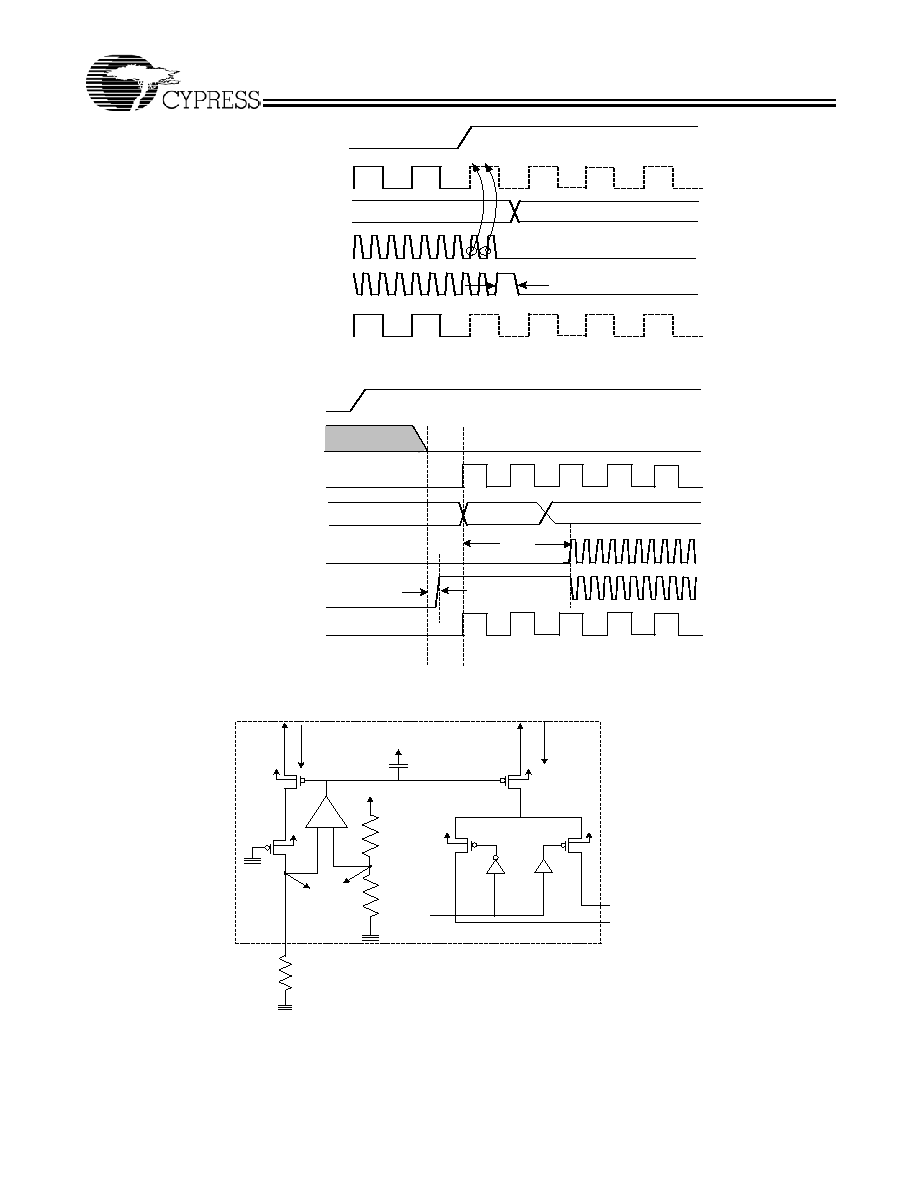
PWRDWN (Power-down) Clarification
The PWRDWN (Power-down) pin is used to shut off the clock
prior to shutting off power to the device. PWRDWN is an
asynchronous active HIGH input. This signal is synchronized
internally to the device powering down the clock synthesizer.
PWRDWN also is an asynchronous function for powering up
the system. When PWRDWN is high, all clocks are tri-stated
and the oscillator and PLL are also powered down. All clocks
are shut down in a synchronous manner so has not to cause
glitches while transitioning to the stopped state. The CLKIN
input must be on and within specified operating parameters
before PWRDWN is asserted and it must remain in this state
while PWRDWN is asserted, see Figure 1.
When PWRDWN is de-asserted (CLKIN starts after
powerdown de-assertion to meet the IDD
250µA specifi-
cation) the clocks should remain stopped until the VCO is
stable and within specification (t
STABLE
)., see Figure 2.
Byte1[7:2] Control Register
Bit
@Pup
Pin#
Name
Pin Description
7
0
Reserved set equal to `0'
6
0
Reserved set equal to `0'
5
0
Reserved set equal to `0'
4
0
Reserved set equal to `0'
3
0
Reserved set equal to `0'
2
1
11,12
CLKEN
CLKOUT/CLKOUT# enable
0 =Disable, 1 = Enable
Byte 1: [1:0] Control Register (Charge Pump Settings)
Bit
@Pup
Default Value
One Step Higher Than Default
Two Steps Higher Than Default
1
0
0
1
1
0
0
0
1
0
Byte 6: Vendor/Revision ID Register
Bit
@Pup
Pin#
Name
Pin Description
7
0
≠
≠
Revision ID Bit 3
6
0
≠
≠
Revision ID Bit 2
5
0
≠
≠
Revision ID Bit 1
4
0
≠
≠
Revision ID Bit 0
3
1
≠
≠
Vendor ID Bit 3
2
0
≠
≠
Vendor ID Bit 2
1
0
≠
≠
Vendor ID Bit 1
0
0
≠
≠
Vendor ID Bit 0
CY25823
Document #: 38-07579 Rev. *C
Page 6 of 12
R E F O U T
T p H Z
P W R D W N
C L K IN
O ff
O n
C lo c k V C O
C L K O U T
C L K O U T #
Figure 1. Power-down Assertion
REFOUT
CLKIN
Off
Clock VCO
CLKOUT
CLKOUT#
Tstable
Starting
Stable
VDD
PWRDWN
TpZH
Figure 2. Power-down Deassertion
C LK OUT
C LK OUT #
I
O U T
C 1
3.3V
2R
R
R
R E F
I
R E F
M
IR E F
V
REF
1.1V
+
-
Figure 3. Current Reference Circuit

CY25823
Document #: 38-07579 Rev. *C
Page 7 of 12
CLKOUT/CLKOUT# Enable Clarification
The CLKOUT enable I2C register bit (Byte1, bit2) is used to
enable/disable the CLKOUT clock. The PLL and crystal oscil-
lator remains on when the outputs are disabled.
When CLKOUT is disabled, the disabled clock is three-stated.
The transition to this mode (three-state) is glitch free. Similarly,
when CLKOUT is enabled the clock starts in a predictable
manner without any glitches or abnormal behavior.
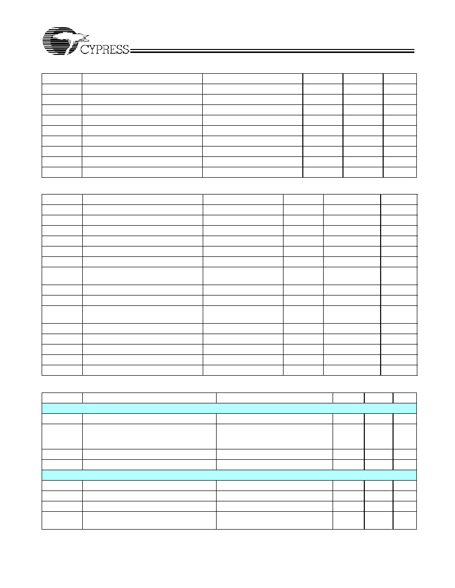
Current Reference, IREF
The details of the current reference circuit are shown in
Figure 3. The operational amplifier in the current reference
circuit drives the gate of M
IREF
with feedback to establish
V
REF
= 1.1V at both inputs of the amplifier. Thus the reference
current is established according to the following formula:
I
REF
= 1.1V / R
REF
where R
REF
is the external resistor and 1.1V is the reference
voltage.
The I
REF
is scaled by 6x at the output stage and I
OUT
is given
as: I
OUT
= 6 x I
REF
.
The recommended value for R
REF
is 475 Ohms, which corre-
sponds to the I
REF
of 2.32mA.
CY25823
Document #: 38-07579 Rev. *C
Page 8 of 12
Absolute Maximum Conditions
Parameter
Description
Condition
Min.
Max.
Unit
V
DD
Core Supply Voltage
≠0.5
4.6
V
V
DDA
Analog Supply Voltage
≠0.5
4.6
V
V
IN
Input Voltage
Relative to V
SS
≠0.5
V
DD
+ 0.5
VDC
T
S
Temperature, Storage
Non-functional
≠65
150
∞C
T
A
Temperature, Operating Ambient
Functional
0
70
∞C
T
J
Temperature, Junction
Functional
≠
150
∞C
ÿ
JC
Dissipation, Junction to Case
Mil-Spec 883E Method 1012.1
≠
33.89
∞C/W
ÿ
JA
Dissipation, Junction to Ambient
JEDEC (JESD 51)
≠
117.36
∞C/W
ESD
HBM
ESD Protection (Human Body Model)
MIL-STD-883, Method 3015
2000
≠
V
DC Electrical Specifications
Parameter
Description
Condition
Min.
Max.
Unit
VDD
Power supply for logic and outputs
3.3 ± 5%
3.135
3.465
V
VDDA
Power supply for PLL
3.3 ± 5%
3.135
3.465
V
V
ILI2C
Input Low Voltage
SDATA, SCLK
V
SS
≠0.5
0.8
V
V
IHI2C
Input High Voltage
SDATA, SCLK
2.0
V
DD
V
V
IL
Input Low Voltage
V
SS
≠ 0.5
0.8
V
V
IH
Input High Voltage
2.0
V
DD
V
I
IL
Input Leakage Current
except internal pull-ups
resistors, 0 < V
IN
< V
DD
≠5
5
µA
I
OZ
High-impedance Output Current
≠10
10
µA
I
DD
Dynamic Supply Current
without output load
≠
50
mA
I
DDS
Total Power Supply Current in Shutdown
mode (No Input Clock)
Shutdown active
≠
250
µA
C
IN
Input Pin Capacitance
2
5
pF
C
OUT
Output Pin Capacitance
3
6
pF
L
IN
Input Pin Inductance
≠
5
nH
R
PU
SCLK and SDATA pull-up resistors
when PWRDWN = 1
50
200
k
R
REF
I
REF
external reference resistor
1% tolerance
200
500
W
AC Electrical Specifications
Parameter
Description
Condition
Min.
Max.
Unit
CLKIN/REFOUT AC Specifications
T
DC
Duty Cycle
Measured at 1.5V crossing point
40
60
%
T
R
/ T
F
Rise and Fall Times
Measured between 0.8V
and 2.0V
(REFOUT with max. 30 pF Lumped
capacitive load)
≠
1.2
ns
T
CCJ
Cycle to Cycle Jitter
As an average over 1-
µs duration
≠
1000
ps
L
ACC
Long-term Accuracy
Over 150 ms
≠
300
ppm
CLKOUT/CLKOUT# AC Specifications
T
DC
CLKOUT and CLKOUT# Duty Cycle
Measured at crossing point V
OX
45
55
%
T
PERIOD
100 MHz CLKOUT and CLKOUT# Period
Measured at crossing point V
OX
9.990
10.010
ns
T
PERIOD
96 MHz CLKOUT and CLKOUT# Period
Measured at crossing point V
OX
10.406
10.427
ns
T
CCJ
CLKOUT/CLKOUT# Cycle to Cycle Jitter
with Spread Spectrum Enabled
Measured at crossing point V
OX
≠
200
ps
CY25823
Document #: 38-07579 Rev. *C
Page 9 of 12
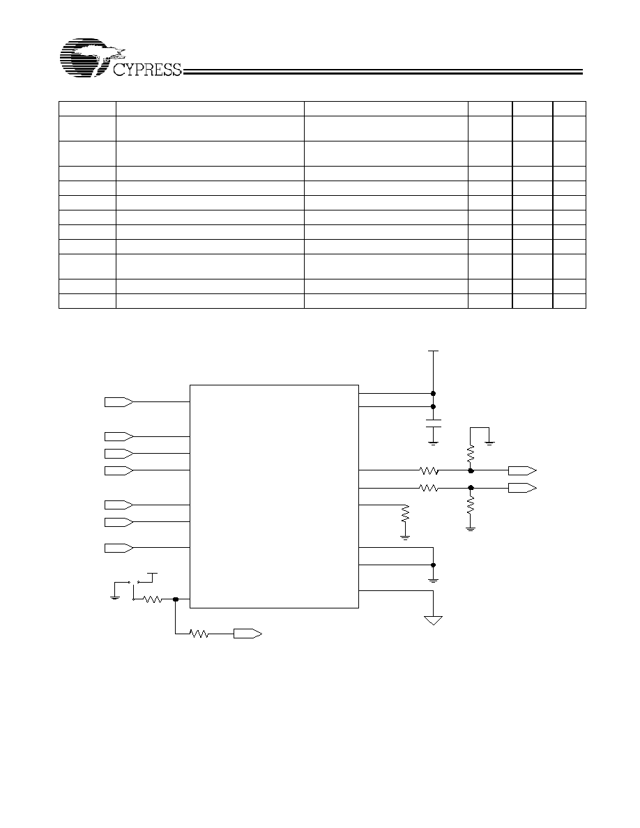
Application Schematic
[2,3]
Notes:
1. Not 100% tested, guaranteed by design.
2. V
DD
and V
DDA
should be tied together and connected to 3.3V.
3. V
SSIREF
and V
SS
are tied together and are common ground.
T
R
/ T
F
CLKOUT and CLKOUT# Rise and Fall Times Measured from V
OL
= 0.175 to
V
OH
= 0.525V
175
700
ps
T
RFM
Rise/Fall Matching
Determined as a fraction of
2*(T
R
≠ T
F
)/(T
R
+ T
F
)
≠
20
%
Tstable
[1]
All clock stabilization from Power-up
≠
3.0
ms
T
R
Rise Time Variation
≠
125
ps
T
F
Fall Time Variation
≠
125
ps
V
HIGH
Voltage High
660
850
mv
V
LOW
Voltage Low
≠150
≠
mv
V
OX
Crossing Point Voltage at 0.7V Swing
250
550
mv
V
OVS
Maximum Overshoot Voltage
≠
V
HIGH
+
0.3
V
V
UDS
Minimum Undershoot Voltage
≠0.3
≠
V
V
RB
Ring Back Voltage
Measure SE
≠
0.2
V
AC Electrical Specifications
(continued)
Parameter
Description
Condition
Min.
Max.
Unit
V DDA
V DD
V DD
0.1
µF
CLKOUT
CLKOUT#
16
9
12
11
33
33
IREF
475
V SSIREF
V SS
V SSA
Separate Ground
14
13
10
15
10
V DD
REFOUT/SEL
33
PW RDW N
5
6
SCLOCK
SDA TA
CLKIN
S2
S3
S1
7
8
4
3
1
2
R1
R2
R3
R4
R5
C1
49.9
49.9
1%
R7
R6
1%
1%
5%
5%
5%
5%
Source
Termination
Figure 4. Application Schematic
CY25823
Document #: 38-07579 Rev. *C
Page 10 of 12
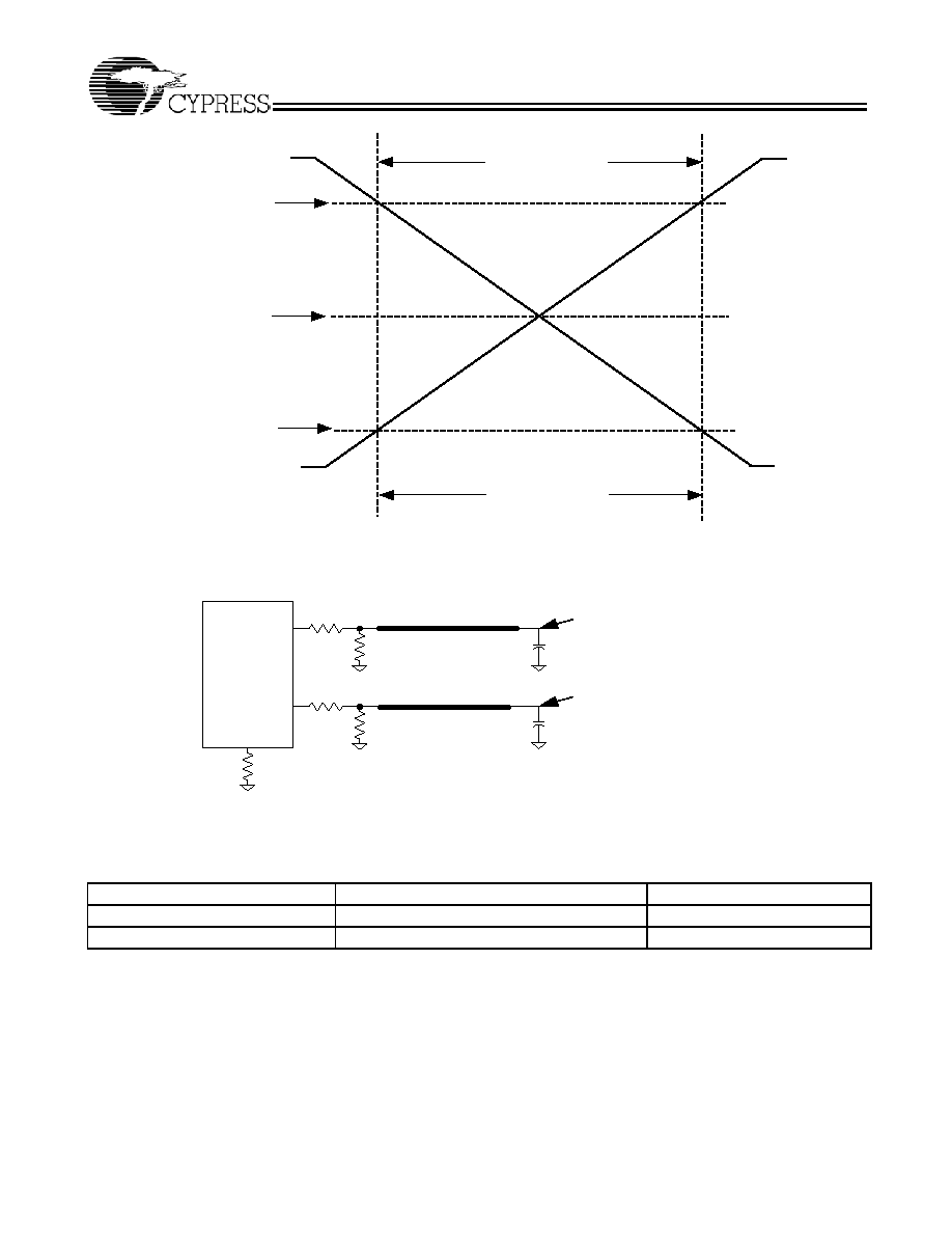
Figure 5. Single-ended Measurement Points for TRise and TFall (CLKOUT and CLKOUT#)
V
OH
= 0.525V
TRise (CLCKOUT)
TFall (CLCKOUT)
CLK
OUT
#
V
OL
= 0.175V
VCROSS
CL
KO
UT
C L K O U T
T
P C B
T
P C B
C L K O U T #
33
33
49.9
49.9
M e a s u re m e n t
P o in t
2 p F
475
IR E F
M e a s u re m e n t
P o in t
2 p F
Figure 6. 0.7V Load Configuration
Ordering Information
Part Number
Package Type
Product Flow
CY25823ZXC
16-pin TSSOP (Lead-free)
Commercial, 0∞C to 70∞C
CY25823ZXCT
16-pin TSSOP ≠ Tape and Reel (Lead-free)
Commercial, 0∞C to 70∞C
CY25823
Document #: 38-07579 Rev. *C
Page 11 of 12
© Cypress Semiconductor Corporation, 2004. The information contained herein is subject to change without notice. Cypress Semiconductor Corporation assumes no responsibility for the use
of any circuitry other than circuitry embodied in a Cypress product. Nor does it convey or imply any license under patent or other rights. Cypress products are not warranted nor intended to be
used for medical, life support, life saving, critical control or safety applications, unless pursuant to an express written agreement with Cypress. Furthermore, Cypress does not authorize its
products for use as critical components in life-support systems where a malfunction or failure may reasonably be expected to result in significant injury to the user. The inclusion of Cypress
products in life-support systems application implies that the manufacturer assumes all risk of such use and in doing so indemnifies Cypress against all charges.
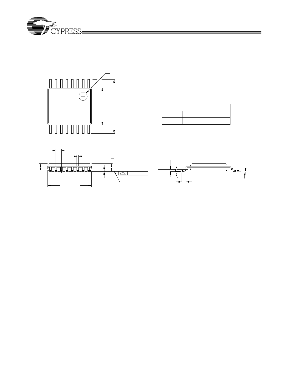
Package Drawing and Dimension
All product and company names mentioned in this document are the trademarks of their respective holders.
4.90[0.193]
1.10[0.043] MAX.
0.65[0.025]
0.20[0.008]
0.05[0.002]
16
PIN 1 ID
6.50[0.256]
SEATING
PLANE
1
0.076[0.003]
6.25[0.246]
4.50[0.177]
4.30[0.169]
BSC.
5.10[0.200]
0.15[0.006]
0.19[0.007]
0.30[0.012]
0.09[[0.003]
BSC
0.25[0.010]
0∞-8∞
0.70[0.027]
0.50[0.020]
0.95[0.037]
0.85[0.033]
PLANE
GAUGE
DIMENSIONS IN MM[INCHES] MIN.
MAX.
REFERENCE JEDEC MO-153
PACKAGE WEIGHT 0.05 gms
PART #
Z16.173
STANDARD PKG.
ZZ16.173 LEAD FREE PKG.
16-lead TSSOP 4.40 MM Body Z16.173
51-85091-*A
CY25823
Document #: 38-07579 Rev. *C
Page 12 of 12
Document History Page
Document Title: CY25823 CK-SSCD Spread Spectrum Differential Clock Specification
Document #: 38-07579 Rev. *C
Rev.
ECN No.
Issue Date
Orig. of Change
Description of Change
**
131662
12/10/03
RGL
New Data Sheet
*A
203801
See ECN
RGL
Fixed the I2C Block Read/Write Protocol and Byte
Read/Write Protocol tables
*B
252269
See ECN
RGL
Corrected to New Lead Free Code
*C
260155
See ECN
RGL
Minor Change: Corrected the package diagram