Spread Spectrum Clock Generator
CY25901
Cypress Semiconductor Corporation
∑
3901 North First Street
∑
San Jose
,
CA 95134
∑
408-943-2600
Document #: 38-07521 Rev. **
Revised February 18, 2003
Features
∑ Supports clock requirements for Spread Spectrum
∑ 40-MHz Spread Spectrum clock output
∑ Reference clock output
∑ Two spread bandwidths: 1%, 3%
∑ External clock or Cera-Lock input
∑ 3.3V operation
∑ 8-pin SOIC package
Description
The CY25901 clock generator provides a low-electromagnetic
interference (EMI) clock output. It features Spread Spectrum
technology, a modulation technique designed specifically for
reducing EMI at the fundamental frequency and its harmonics.
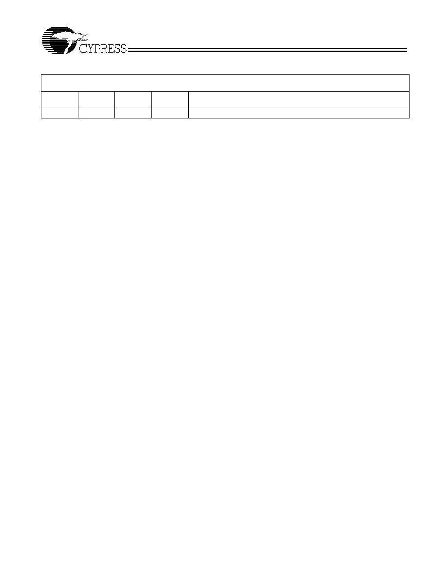
Table 1. Function Table
SSSEL
SSON
REFOUT
CLKOUT (Spread Spectrum)
CY25901SC
CY25901SC-1
0
0
XIN
= XIN ± 0.35% (0.7% center)
= XIN ± 0.5% (1.0% center)
1
0
XIN
= XIN ± 1.20% (2.4% center)
= XIN ± 1.5% (3.0% center)
X (don't care)
1
XIN
= XIN (No Spread)
= XIN (No Spread)
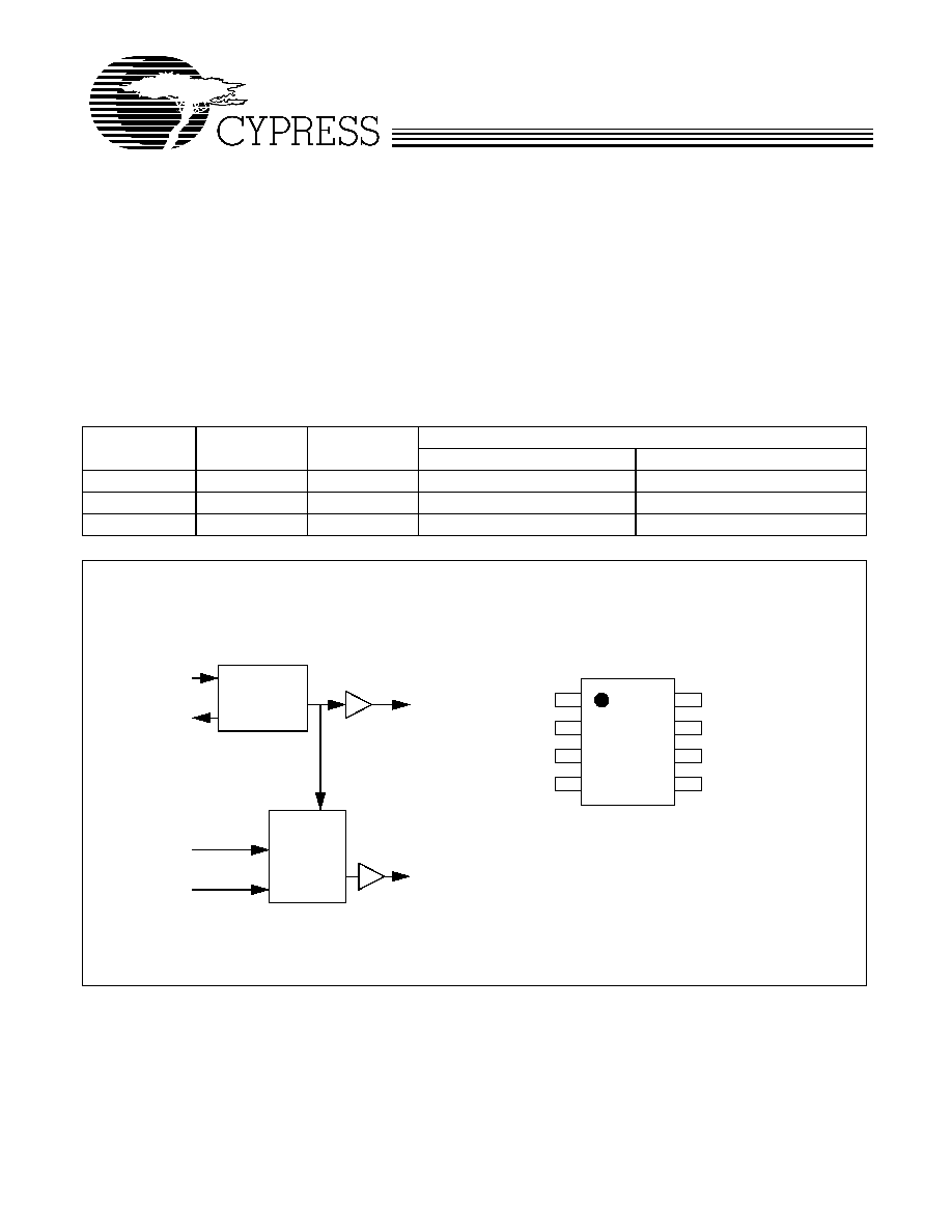
Block Diagram
Pin Configuration
Oscillator
PLL
SSCG
XIN
XOUT
SSSEL
REFOUT
CLKOUT
SSON
CLKOUT
VDD
VSS
XIN
SSON#
REFOUT
SSSEL
XOUT
1
2
3
4
8
7
6
5
CY25901
Document #: 38-07521 Rev. **
Page 2 of 5
Spread Spectrum Clock Generator
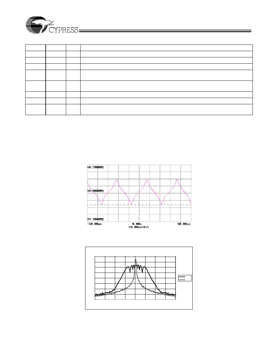
Spread Spectrum Clock Generator (SSCG) is a frequency
modulation technique used to reduce EMI radiation generated
by repetitive digital signals, mainly clocks. A clock radiates EM
energy at its fundamental frequency as well as its harmonics.
Spread Spectrum distributes this energy over a small
frequency bandwidth, and decreasing the peak value of
radiated energy over the spectrum. This technique is achieved
by modulating the clock around or below the center of its
reference frequency by a certain percentage (which also
determines the energy distribution bandwidth).
The SSCG function is enabled when SSON pin is set to low.
Resulting in a spread bandwidth that is center spread, amount
as selected by SSSEL (see Table 1).
Pin Description
Pin No.
Name
I/O
Description
1
CLKOUT
O
Spread Spectrum Clock Output. See Table 1 for frequency selections.
2
VDD
PWR
Power Supply.
3
VSS
PWR
Common Ground.
4
XIN
I
Oscillator Buffer Input. Connect to an external parallel resonant crystal or externally generated
reference clock.
5
XOUT
O
Oscillator Buffer Output. Connect to an external parallel resonant crystal. Do not connect when
an externally generated reference clock is applied at XIN.
6
SSSEL
I
Spread Spectrum Select Input. See Table 1. internally pulled up.
7
REFOUT
O
Buffered Output of XIN.
8
SSON#
I
Spread Spectrum Enable Input. When asserted low, Spread Spectrum is enabled.
Internally pulled down.
Figure 1. Modulation Frequency Profile
Spread Spectrum
-80
-70
-60
-50
-40
-30
-20
-10
0
38
38
39
39
40
41
41
42
43
Frequency(MHz)
dBm
SS-O N
SS-O FF
Figure 2. Spread Spectrum
CY25901
Document #: 38-07521 Rev. **
Page 3 of 5
Absolute Maximum Ratings
Parameter
Description
Condition
Min.
Max.
Unit
V
DD
Core Supply Voltage
≠0.5
4.6
V
V
IN
Input Voltage
Relative to V
SS
≠0.5
V
DD
+0.5
VDC
T
S
Temperature, Storage
Non Functional
≠65
150
∞C
T
A
Temperature, Operating Ambient
Functional
≠10
85
∞C
T
J
Temperature, Junction
Functional
≠
150
∞C
ESD
HBM
ESD Protection (Human Body Model)
MIL-STD-883, Method 3015
2000
≠
V
UL≠94
Flammability Rating
@1/8 in.
V≠0
MSL
Moisture Sensitivity Level
1
DC Specifications
Parameter
Description
Condition
Min.
Typ.
Max.
Unit
V
DD
Operating Voltage
3.3V @ ±10%
2.97
3.3
3.63
V
V
IL
Input Low Voltage
[1]
SSON# and SSSEL
≠
≠
0.8
V
V
IH
Input High Voltage
[1]
Inputs
2.2
≠
≠
V
VthXIN
XIN Threshold Voltage
XIN
0.3*VDDC
0.5*VDDC
0.7*VDDC
V
I
DD
Dynamic Supply Current
V
DD
= 3.3V and CL = 0
≠
20
25
mA
I
IL
Input Low Current
SSSEL = VSS
≠55
≠30
≠
µ
A
I
IH
Input High Current
SSON = V
DD
≠
30
55
µ
A
V
OL
Output Low Voltage
I
OL
= 4.0 mA
≠
≠
0.4
V
V
OH
Output High Voltage
I
OH
= ≠4.0 mA
2.4
≠
≠
V
C
IN
Input Capacitance
SSON# and SSSEL Inputs
≠
5
10
pF
C
X
XIN, XOUT Capacitance
[2]
XIN and XOUT
≠
5
≠
pF
PU/PD
Pull-up/Pull-down Resistance
[1]
SSON# and SSSEL Inputs
50
100
200
k
AC Specifications
[3]
Parameter
Description
Condition
Min.
Typ.
Max.
Unit
F
IR
Input Frequency Range
36
40
44
MHz
E
RXIN
XIN Edge Rate
XIN driven by external clock
≠
1
≠
V/nS
T
DCXIN
XIN Duty Cycle
XIN driven by external clock
40
50
60
%
T
R
Outputs Rise Time
[4]
REFOUT, CLKOUT
≠
≠
3
ns
T
F
Outputs Fall Time
[4]
REFOUT, CLKOUT
≠
≠
3
ns
BW%1
CY25901SC, Spread %
SSON=0,SSSEL = 0
0.5
0.7
0.9
%
BW%2
CY25901SC, Spread %
SSON=0,SSSEL = 1
1.7
2.4
3.1
%
BW%3
CY25901SC≠1, Spread %
SSON=0,SSSEL = 0
0.7
1
1.3
%
BW%4
CY25901SC≠1, Spread %
SSON=0,SSSEL = 1
2.1
3
3.9
%
T
PU
Power up to Stable Output
[5]
All output clocks
≠
≠
3
ms
T
DC
CLKOUT Duty Cycle
[5]
CL = 15pF
45
50
55
%
T
CCJ
REFOUT Cycle to Cycle jitter
[5]
CL = 15pF
≠
110
200
ps
T
CCJ
CLKOUT Cycle to Cycle jitter
[5]
CL = 15pF
≠
110
200
ps
Fmod
Frequency Modulation Rate
SSON# = GND Internally pulled down
≠
31
≠
kHz
Notes:
1.
SSSEL has internal pull-up and SSON has pull-down resistors.
2.
In applications if a crystal is used for the input reference clock, refer to crystal manufacturer's specifications for the required crystal load capacitor value.
3.
Parameters are guaranteed by design and characterization. Not 100% tested in production. All parameters specified with fully loaded outputs. All outputs
loaded with 15 pF.
4.
Measured between 0.2*VDD and 0.8*VDD Volts.
5.
Triggering is done at 1.5V VDDC.
CY25901
Document #: 38-07521 Rev. **
Page 4 of 5
© Cypress Semiconductor Corporation, 2003. The information contained herein is subject to change without notice. Cypress Semiconductor Corporation assumes no responsibility for the use
of any circuitry other than circuitry embodied in a Cypress Semiconductor product. Nor does it convey or imply any license under patent or other rights. Cypress Semiconductor does not authorize
its products for use as critical components in life-support systems where a malfunction or failure may reasonably be expected to result in significant injury to the user. The inclusion of Cypress
Semiconductor products in life-support systems application implies that the manufacturer assumes all risk of such use and in doing so indemnifies Cypress Semiconductor against all charges.
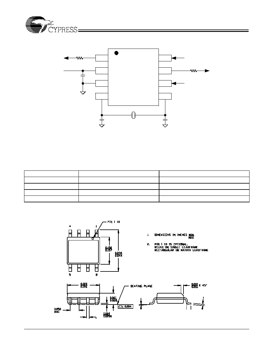
Application Schematic
Use crystal or cera-lock filter manufacturer's recommended
values for CL1 and CL2 load capacitors. 0.1-
µ
F bypass
capacitor for power pins should always be used and placed
close to their V
DD
pin. R1 and R2 are series termination
resistors for impedance matching.
Package Drawing and Dimensions
All product and company names mentioned in this document are the trademarks of their respective holders.
1
2
3
4
8
7
6
5
CLKOUT
VDD(3.3V)
REFOUT
XIN
XOUT
SSSEL
CL1
CL2
SSON#
REFOUT
CLKOUT
VDD
VSS
R1
R2
XTAL
0.1
µ
F
Figure 3. Application Schematic
Ordering Information
Part Number
Package Type
Production Flow
CY25901SC≠1
8-pin SOIC
Commercial, ≠10
∞
C to +85
∞
C
CY25901SC≠1T
8-pin SOIC ≠ Tape and Reel
Commercial, ≠10
∞
C to +85
∞
C
CY25901SC
8-pin SOIC
Commercial, ≠10
∞
C to +85
∞
C
CY25901SCT
8-pin SOIC ≠Tape and Reel
Commercial, ≠10
∞
C to +85
∞
C
8-lead (150-Mil) SOIC S8
51-85066-A
CY25901
Document #: 38-07521 Rev. **
Page 5 of 5
Document History Page
Document Title: CY25901 Spread Spectrum Clock Generator
Document Number: 38-07521
REV.
ECN NO.
Issue Date
Orig. of
Change
Description of Change
**
124075
02/19/03
RGL
New Data Sheet