 | –≠–ª–µ–∫—Ç—Ä–æ–Ω–Ω—ã–π –∫–æ–º–ø–æ–Ω–µ–Ω—Ç: CY26049-1 | –°–∫–∞—á–∞—Ç—å:  PDF PDF  ZIP ZIP |
ADVANCE
INFORMATION
FailSafeTM
Communications Clock Generator
CY26049-1
Cypress Semiconductor Corporation
∑
3901 North First Street
∑
San Jose
∑
CA 95134
∑
408-943-2600
Document #: 38-07488 Rev. **
Revised October 31, 2002
Features
Benefits
∑ Fully integrated phase-locked loop (PLL)
∑ Integrated high-performance PLL tailored for telecom-
munications frequency synthesis eliminates the need
for external loop filter components
∑ FailSafeTM output
∑ When reference is off, DCXO maintains clock outputs
and SAFE pin indicates FailSafe conditions
∑ PLL driven by a crystal oscillator
∑ DCXO maintains continuous operation should the input
reference clock fail
∑ Glitch-free transition simplifies system design
∑ Two 6.312-MHz outputs from 8-kHz input
∑ Works with commonly available, low-cost 18.432-MHz
crystal
∑ Low-jitter, high-accuracy outputs
∑ Zero-ppm error for all output frequencies
∑ 3.3 V ± 5% operation
∑ Compatibility across industry standard design
platforms
∑ 16-lead TSSOP
∑ Industry standard package with 6.4 x 5.0 mm footprint
and a height profile of just 1.1 mm
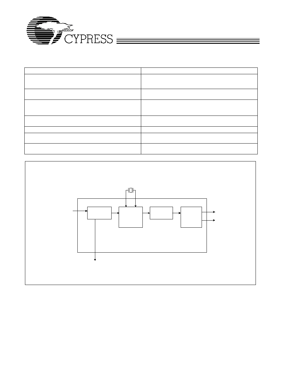
Logic Block Diagram
CLKB
6.312 MHz
XIN
XOUT
ICLK
CLKA
6.312 MHz
SAFE
input reference clock
(typical 8 kHz)
external pullable crystal
(18.432 MHz)
DIGITAL
CONTROLED
CRYSTAL
OSCILLATOR
FAILSAFE
TM
CONTROL
PHASE
LOCKED
LOOP
OUTPUT
DIVIDERS
ICLK detected
ADVANCE
INFORMATION
CY26049-1
Document #: 38-07488 Rev. **
Page 2 of 4
Description
CY26049 is a FailSafe frequency synthesizer with a reference
clock input and 6.312-MHz output. The device provides an
optimum solution for applications where continuous operation
is required in the event of a primary clock failure. The
continuous, glitch-free operation is achieved by using a
DCXO, which serves as a primary clock source. The FailSafe
control circuit synchronizes the DCXO oscillator with the
reference as long as the reference is within the pull range of
the crystal.
In the event of a reference clock failure the DCXO maintains
the last frequency of the reference clock. The unique feature
of the CY26049-1 is that the DCXO is in fact the primary
clocking source. When the reference clock is restored, the
DCXO automatically resynchronizes to the reference. The
status of the reference clock input, as detected by the
CY26049-1, is reported by the SAFE pin.
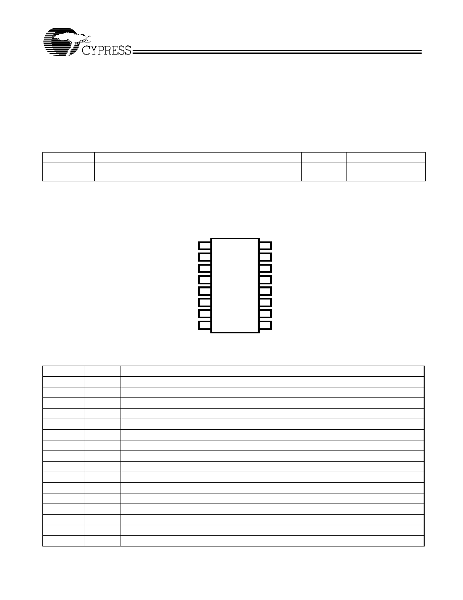
Pin Configuration
Selector Guide
Part Number
Input Frequency Range
Outputs
Output Frequencies
CY26049ZC-1 Reference Input Clock: 8 kHz
Crystal: 18.432-MHz pullable Crystal per Cypress Specification
2
6.312 MHz
CY26049-1
16-pin TSSOP
Top View
ICLK 1
16 NC
NC
2
15 CLKB
NC
3
14 NC
NC
4
13 NC
VDD
5
12 VDD
VSS
6
11 VSS
CLKA
7
10 SAFE
XIN
8
9 XOUT
Pin Description
Pin Number Pin Name
Pin Description
1
ICLK
Reference Input Clock--8-kHz clock
2
NC No
Connect
3
NC
No Connect
4
NC
No Connect
5
VDD
Connect to 3.3V power supply
6
VSS
Ground
7
CLKA
Clock Output; 6.312 MHz
8
XIN
18.432-MHz Pullable Crystal Input
9
XOUT
18.432-MHz Pullable Crystal Output
10
SAFE
High = reference ICLK within range, Low = reference ICLK out of range
11
VSS
Ground
12
VDD
Connect to 3.3V power supply.
13
NC
No Connect
14
NC
No Connect
15
CLKB
Clock Output; 6.312 MHz
16
NC
No Connect
ADVANCE
INFORMATION
CY26049-1
Document #: 38-07488 Rev. **
Page 3 of 4
© Cypress Semiconductor Corporation, 2002. The information contained herein is subject to change without notice. Cypress Semiconductor Corporation assumes no responsibility for the use
of any circuitry other than circuitry embodied in a Cypress Semiconductor product. Nor does it convey or imply any license under patent or other rights. Cypress Semiconductor does not authorize
its products for use as critical components in life-support systems where a malfunction or failure may reasonably be expected to result in significant injury to the user. The inclusion of Cypress
Semiconductor products in life-support systems application implies that the manufacturer assumes all risk of such use and in doing so indemnifies Cypress Semiconductor against all charges.
Recommended Pullable Crystal Specifications
Ordering Information
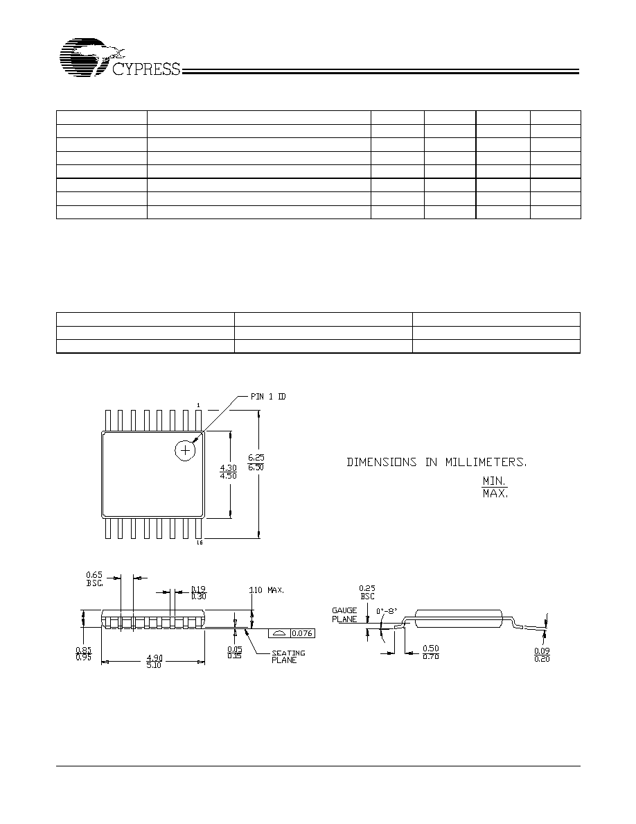
Package Drawing and Dimensions
FailSafe is a trademark of Cypress Semiconductor Corporation. All product and company names mentioned in this document are
the trademarks of their respective holders.
Parameter
Name
Min.
Typ.
Max.
Unit
CL
XTAL
Crystal Nominal Load Capacitance
14
16
20
pF
C0/C1
250
T
o
Operating Temperature
0
70
∞C
Crystal Accuracy
Crystal Initial Accuracy
±20
±50
ppm
TT
s
Stability Over Temperature and Aging
± 20
±50
ppm
C
O
Shunt Capacitance
5
7
pF
C
LBRD
Stray Capacitance--on XIN/XOUT
2
pF
All applicable DC and AC characteristic are as described in the CY26049-36 data sheet.
Ordering Code
Package Type
Operating Temperature Range
CY26049ZC-1
16-lead TSSOP
Commercial 0 to 70∞C
CY26049ZC-1T
16-lead TSSOP--Tape and Reel
Commercial 0 to 70∞C
16-lead Thin Shrunk Small Outline Package (4.40 MM Body) Z16
51-85091-**

ADVANCE
INFORMATION
CY26049-1
Document #: 38-07488 Rev. **
Page 4 of 4
Document History Page
Document Title: CY26049-1 FailSafeTM Communications Clock Generator
Document Number: 38-07488
REV.
ECN NO.
Issue
Date
Orig. of
Change
Description of Change
**
120007
11/01/02
CKN
New Data Sheet