PRELIMINARY
FailSafeTM PacketClockTM Global
Communications Clocks
CY26049-36
Cypress Semiconductor Corporation
∑
3901 North First Street
∑
San Jose
∑
CA 95134
∑
408-943-2600
ADocument #: 38-07415 Rev. *A
Revised December 20, 2002
Features
Benefits
∑ Fully integrated phase locked loop (PLL)
∑ Integrated high-performance PLL tailored for telecom-
munications frequency synthesis eliminates the need
for external loop filter components
∑ FailSafe
output
∑ When reference is in range, clock outputs are phase
aligned with reference. SAFE pin is high.
∑ When reference is off, DCXO maintains clock outputs.
SAFE pin is low.
∑ PLL driven by a crystal oscillator, phase aligned with
external reference
∑ DCXO maintains continuous operation should the input
reference clock fail
∑ Glitch-free transition simplifies system design
∑ Output frequencies selectable and/or programmed to
standard communication frequencies
∑ Selectable output clock rates include T1/DS1, E1,
T3/DS3, E3, and OC-3.
∑ Works with commonly available, low-cost 18.432-MHz
crystal
∑ Low-jitter, high-accuracy outputs
∑ Zero-ppm error for all output frequencies
∑ Commercial and Industrial operation
∑ Performance guaranteed for applications that require
an extended temperature range
∑ 3.3 V ± 5% operation
∑ Compatibility across industry standard design
platforms
∑ 16-lead TSSOP
∑ Industry standard package with 6.4 x 5.0 mm footprint
and a height profile of just 1.1 mm
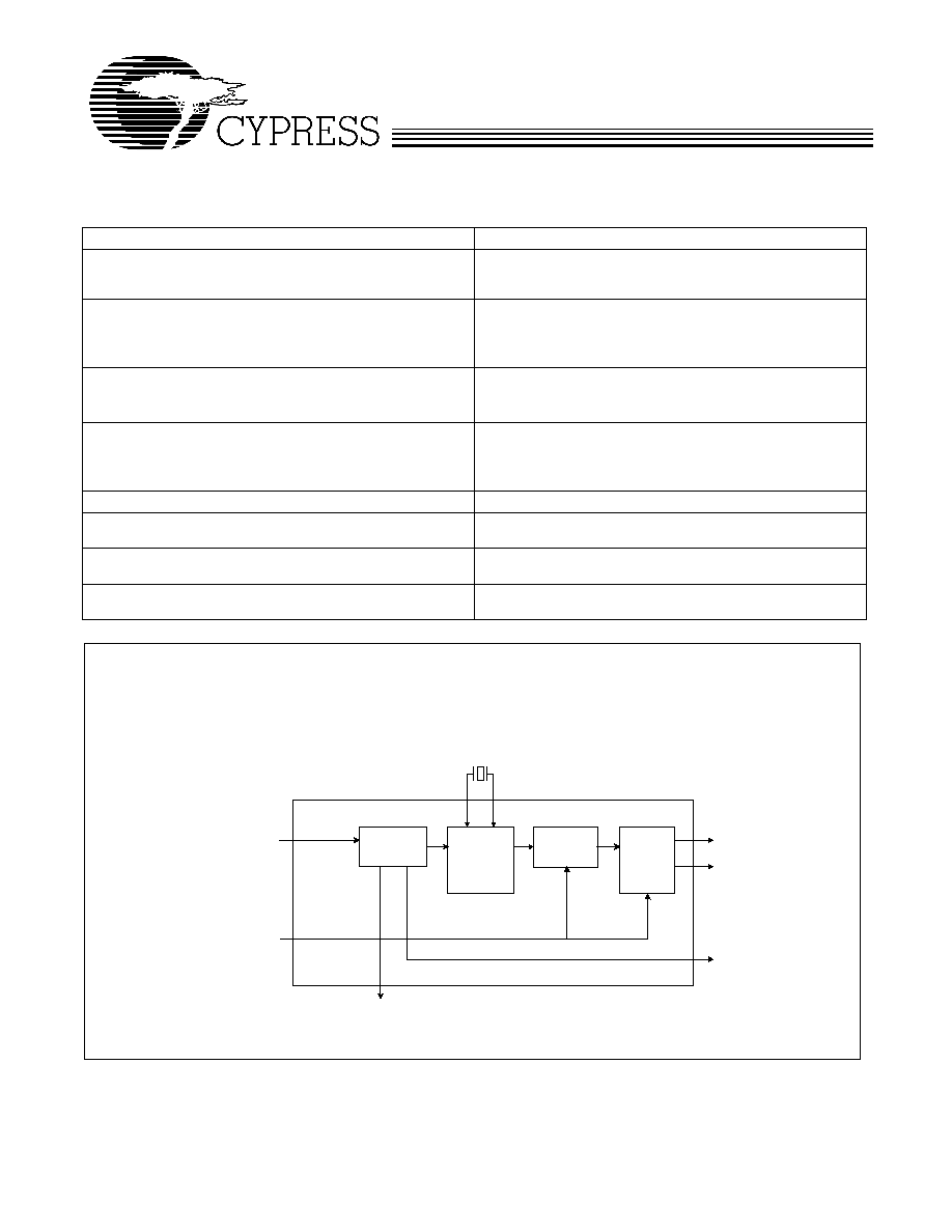
Logic Block Diagram
CLK/2
FS[3:0]
XIN
XOUT
ICLK
CLK
SAFE
frequency select
input reference
(typical 8 kHz)
external pullable crystal
(18.432 MHz)
8K
DIGITAL
CONTROLLED
CRYSTAL
OSCILLATOR
FAILSAFE
TM
CONTROL
PHASE
LOCKED
LOOP
OUTPUT
DIVIDERS
High=ICLK detected
PRELIMINARY
CY26049-36
Document #: 38-07415 Rev. *A
Page 2 of 7
Description
CY26049 is a FailSafe frequency synthesizer with a reference
clock input and three phase-aligned outputs. The device
provides an optimum solution for applications where
continuous operation is required in the event of a primary clock
failure. The continuous, glitch-free operation is achieved by
using a DCXO which serves as a primary clock source. The
FailSafe
TM
control circuit synchronizes the DCXO with the
reference as long as the reference is within the pull range of
the crystal.
In the event of a reference clock failure the DCXO maintains
the last frequency and phase information of the reference
clock. The unique feature of the CY26049-36 is that the DCXO
is in fact the primary clocking source. When the reference
clock is restored, the DCXO automatically re-synchronizes to
the reference. The status of the reference clock input, as
detected by the CY26049-36, is reported by the SAFE pin.
In the buffer mode (FS3:FS0 = 1110 or 1111), the CY26049-36
can be used as a jitter attenuator. In this mode, extensive jitter
on the input clock will be "filtered", resulting in a low-jitter
output clock.
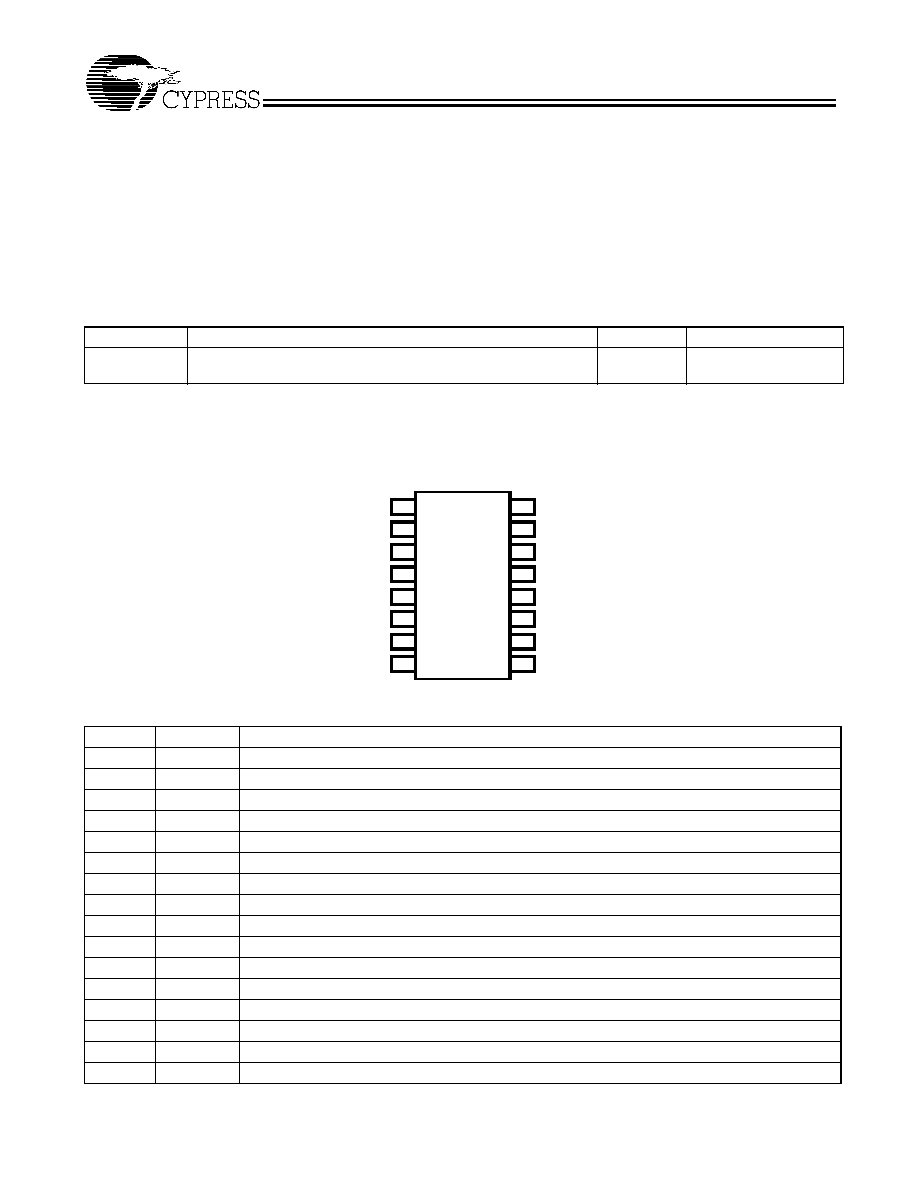
Pin Configuration
Selector Guide
Part Number
Input Frequency Range
Outputs
Output Frequencies
CY26049-36
8 kHz or 10 to 60 MHz Reference Input
CRYSTAL: 18.432-MHz pullable Crystal per Cypress Specification
3
8 kHz to 155.52 MHz
Selectable (see Table 1)
ICLK
1
16 N/C
8K
2
15 CLK
FS1
3
14 FS0
FS2
4
13 FS3
VDD
5
12 VDD
VSS
6
11 VSS
CLK/2
7
10 SAFE
XIN
8
9 XOUT
CY26049-36
16-pin TSSOP
Top View
Pin Description Table
Pin Name Pin Number
Pin Description
ICLK
1
Reference Input Clock. 8-kHz or 10- to 60-MHz clock.
8K 2
Clock Output. 8 kHz; high impedance in buffer mode.
FS1
3
Frequency Select 1. Determines CLK outputs per Table 1.
FS2
4
Frequency Select 2. Determines CLK outputs per Table 1.
VDD
5
Connect to 3.3V power supply.
VSS
6
Ground.
CLK/2
7
Clock Output. Frequency per Table 1.
XIN
8
18.432-MHz Pullable Crystal Input.
XOUT
9
18.432-MHz Pullable Crystal Output.
SAFE 10
High = reference ICLK within range, Low = reference ICLK out of range or failed.
VSS
11
Ground.
VDD
12
Connect to 3.3V power supply.
FS3
13
Frequency Select 3. Determines CLK outputs per Table 1.
FS0
14
Frequency Select 0. Determines CLK outputs per Table 1.
CLK
15
Clock Output. Frequency per Table 1.
N/C
16
No connect .
PRELIMINARY
CY26049-36
Document #: 38-07415 Rev. *A
Page 3 of 7
Frequency Select Tables
Table 1. CY24049-36 Frequency Select≠Output Decoding Table≠External Mode (MHz except as noted)
ICLK
FS3
FS2
FS1
FS0
CLK/2
CLK
8K
Crystal
8kHz
0
0
0
0
1.544
3.088
8kHz
18.432
8kHz
0
0
0
1
2.048
4.096
8kHz
18.432
8kHz
0
0
1
0
22.368
44.736
8kHz
18.432
8kHz
0
0
1
1
17.184
34.368
8kHz
18.432
8kHz
0
1
0
0
77.76
155.52
8kHz
18.432
8kHz
0
1
0
1
16.384
32.768
8kHz
18.432
8kHz
0
1
1
0
14.352
28.704
8kHz
18.432
8kHz
0
1
1
1
High Z
[1]
High Z
[1]
High Z
[1]
18.432
8kHz
1
0
0
0
18.528
37.056
8kHz
18.432
8kHz
1
0
0
1
12.352
24.704
8kHz
18.432
8kHz
1
0
1
0
7.68
15.36
8kHz
18.432
8kHz
1
0
1
1
High Z
[1]
High Z
[1]
High Z
[1]
18.432
8kHz
1
1
0
0
12.288
24.576
8kHz
18.432
8kHz
1
1
0
1
16.384
32.768
8kHz
18.432
Table 2. CY24049-36 Frequency Select≠Output Decoding Table≠Buffer Mode
ICLK
FS3
FS2
FS1
FS0
CLK/2
CLK
8K
Crystal
20 to 60
1
1
1
0
ICLK/2
ICLK
High Z
[1]
ICLK/2
10 to 30
1
1
1
1
2*ICLK
4*ICLK
High Z
[1]
ICLK
Absolute Maximum Conditions
Parameter
Description
Min.
Max.
Unit
V
DD
Supply Voltage
≠0.5
7.0
V
T
S
Storage Temperature
≠65
125
∞ C
T
J
Junction Temperature
125
∞ C
Digital Inputs
V
SS
≠ 0.3
V
DD
+ 0.3
V
Electrostatic Discharge
> 2,000
V
Recommended Pullable Crystal Specifications
[2]
Parameter
Name
Min.
Typ.
Max.
Unit
CL
XTAL
Crystal Nominal Load Capacitance
14
16
20
pF
C0/C1
250
T
o
Operating Temperature (Commercial Temperature)
0
70
∞ C
T
o
Operating Temperature (Industrial Temperature)
≠40
85
∞ C
Crystal Accuracy
Crystal Initial Accuracy
±20
±50
ppm
TT
s
Stability over Temperature and Aging
± 20
±50
ppm
C
O
Shunt Capacitance
5
7
pF
C
LBRD
Stray Capacitance ≠ on XIN/XOUT
2
pF
Notes:
1.
High Z = high impedence on output.
2.
Ecliptek ECX-5680 18.432M meets these specifications.
PRELIMINARY
CY26049-36
Document #: 38-07415 Rev. *A
Page 4 of 7
Recommended Operating Conditions
Parameter
Description
Min.
Typ.
Max.
Unit
V
DD
Operating Voltage
3.15
3.3
3.45
V
T
AC
Ambient Temperature (Commercial Temperature)
0
70
∞ C
T
AI
Ambient Temperature (Industrial Temperature)
≠40
85
∞ C
C
LOAD
Max Output Load Capacitance
15
pF
DC Electrical Specifications
(Commercial Temp: 0
∞
to 70
∞
C)
Parameter
Description
Test Conditions
Min.
Typ.
Max.
Unit
I
OH
Output High Current
V
OH
= V
DD
≠ 0.5, V
DD
= 3.3V (source)
12
24
mA
I
OL
Output Low Current
V
OL
= 0.5, V
DD
= 3.3V (sink)
12
24
mA
V
IH
Input High Voltage
CMOS Levels
0.7
V
DD
V
IL
Input High Voltage
CMOS Levels
0.3
V
DD
I
I
Input Current
± 5
µ
A
C
IN
Input Capacitance
7
pF
I
OZ
Output Leakage Current
High Z
[3]
output
± 5
µ
A
I
DD
Supply Current
C
LOAD
= 15 pF, V
DD
= 3.45V, FS [3:0]=0100
45
mA
C
LOAD
= 15 pF, V
DD
= 3.45V, FS [3:0]=1101
30
mA
DC Electrical Specifications
(Industrial Temp: ≠40
∞
to 85
∞
C)
Parameter
Description
Test Conditions
Min.
Typ.
Max.
Unit
I
OH
Output High Current
V
OH
= V
DD
≠ 0.5, V
DD
= 3.3V (source)
10
20
mA
I
OL
Output Low Current
V
OL
= 0.5, V
DD
= 3.3V (sink)
10
20
mA
V
IH
Input High Voltage
CMOS Levels
0.7
V
DD
V
IL
Input High Voltage
CMOS Levels
0.3
V
DD
I
I
Input Current
± 5
µ
A
C
IN
Input Capacitance
7
pF
I
OZ
Output Leakage Current
High Z
[3]
output
± 5
µ
A
I
DD
Supply Current
C
LOAD
= 15 pF, V
DD
= 3.45V, FS [3:0] = 0100
50
mA
C
LOAD
= 15 pF, V
DD
= 3.45V, FS [3:0] = 1101
35
mA
AC Electrical Specifications
(Commercial Temp: 0
∞
to 70
∞
C and Industrial Temp: ≠40
∞
to 85
∞
C)
Parameter
Description Test
Conditions
Min.
Typ.
Max.
Unit
f
ICLK-E
Frequency, Input Clock
Input Clock Frequency, External Mode
8.000
kHz
f
ICLK-B
Frequency, Input Clock
Input Clock Frequency, Buffer Mode
10
60
MHz
LR
FailSafe
Lock Range
[4]
Range of reference ICLK for Safe = High
≠250
+250
ppm
tp
ICLK
Pulse Width, Input Clock
Input Clock Pulse Width
3
ns
t
d8K
Propagation Delay
Input Clock Rising Edge to 8K Rising Edge, External
Mode
7
ns
t
dCLK
Delay, CLK to CLK/2
Output Clock (CLK) Rising Edge to Output Clock
(CLK/2) Rising Edge
1
ns
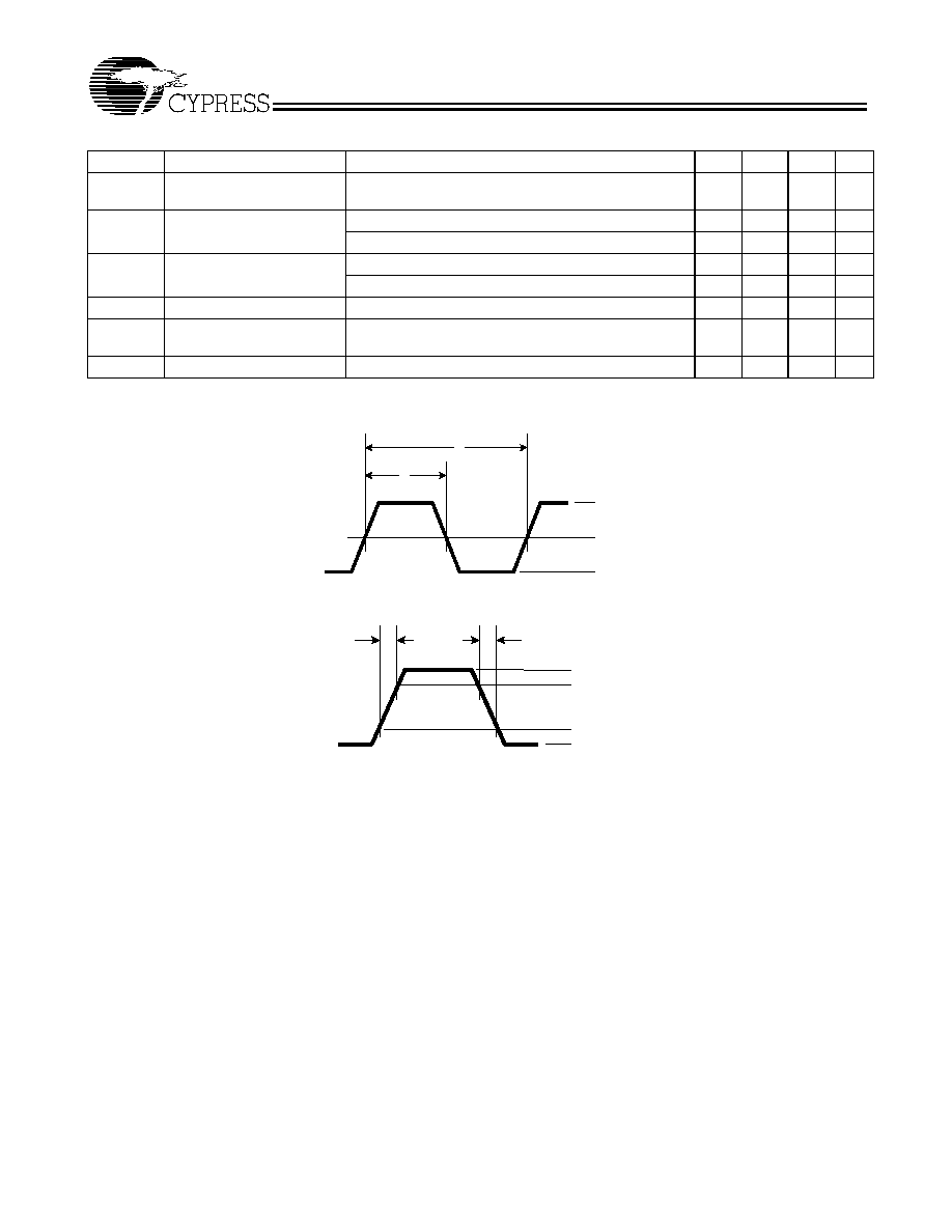
DC = t
2
/t
1
Output Duty Cycle
Duty Cycle as defined in Figure 1, measured at 50% of
V
DD
45
50
55
%
t
3
Rise Time
Output Clock Rise Time, Measured from 20% to 80% of
V
DD
, C
LOAD
= 15 pF See Figure 2
1.4
2.5
ns
Notes:
3.
High Z = high impedence.
4.
Dependent on crystals chosen and and crystal specs.
PRELIMINARY
CY26049-36
Document #: 38-07415 Rev. *A
Page 5 of 7
Voltage and Timing Definitions
t
4
Fall Time
Output Clock Fall Time, Measured from 80% to 20% of
V
DD
, C
LOAD
= 15 pF See Figure 2
1.4
2.5
ns
T
PJIT
Clock Jitter; CLK, CLK/2 > 5
MHz
Period Jitter, Peak to Peak, 10,000 periods
250
ps
RMS Period Jitter, RMS
50
ps
T
PJIT
Clock Jitter; CLK, CLK/2 < 5
MHz
Period Jitter, Peak to Peak, 10,000 periods
500
ps
RMS Period Jitter, RMS
100
ps
t
6
PLL Lock Time
Time for PLL to lock within ± 150 ppm of target frequency
3
ms
t
fs_lock
FailSafe Lock Time
Time for PLL to lock to ICLK (outputs phase aligned with
ICLK and Safe = High)
7
s
f
error
Frequency Synthesis Error
Actual mean frequency error vs. target
0
ppm
AC Electrical Specifications
(Commercial Temp: 0
∞
to 70
∞
C and Industrial Temp: ≠40
∞
to 85
∞
C) (continued)
Parameter
Description Test
Conditions
Min.
Typ.
Max.
Unit
Clock
Output
V
DD
50% of V
DD
0V
t
1
t
2
Figure 1. Duty Cycle Definition
Clock
Output
t
3
t
4
V
DD
80% of V
D D
20% of V
D D
0V
Figure 2. Rise and Fall Time Definitions
PRELIMINARY
CY26049-36
Document #: 38-07415 Rev. *A
Page 6 of 7
© Cypress Semiconductor Corporation, 2002. The information contained herein is subject to change without notice. Cypress Semiconductor Corporation assumes no responsibility for the use
of any circuitry other than circuitry embodied in a Cypress Semiconductor product. Nor does it convey or imply any license under patent or other rights. Cypress Semiconductor does not authorize
its products for use as critical components in life-support systems where a malfunction or failure may reasonably be expected to result in significant injury to the user. The inclusion of Cypress
Semiconductor products in life-support systems application implies that the manufacturer assumes all risk of such use and in doing so indemnifies Cypress Semiconductor against all charges.
Package Diagram
Test Circuit
Ordering Information
FailSafe and PacketClock are trademarks of Cypress Semiconductor. All product and company names mentioned in this document
are the trademarks of their respective holders.
16-Lead Thin Shrunk Small Outline Package (4.40 MM Body) Z16
51-85091-**
0.1uF
VDD
ICLK
0.1uF
VDD
CLK/2
C
LOAD
C
LOAD
C
LOAD
8K
CLK
16
4
3
2
1
9
10
11
12
13
15
14
5
6
7
8
18.432 MHz
Ordering Code
Package Type
Operating Temperature Range
CY26049ZC-36
16-lead TSSOP
Commercial 0 to 70 ∞ C
CY26049ZC-36T
16-lead TSSOP≠Tape and Reel
Commercial 0 to 70 ∞ C
CY26049ZI-36
16-lead TSSOP
Industrial ≠40 to 85 ∞ C
CY26049ZI-36T
16-lead TSSOP≠Tape and Reel
Industrial ≠40 to 85 ∞ C

PRELIMINARY
CY26049-36
Document #: 38-07415 Rev. *A
Page 7 of 7
Document Title: CY26049-36 FailSafeTM PacketClockTM Global Communications Clocks
Document Number: 38-07415
REV.
ECN NO.
Issue
Date
Orig. of
Change
Description of Change
**
114749
08/08/02
CKN
New Data Sheet
*A
120067
01/06/03
CKN
Pg. 6 Changed "FailSafe is a trademark of Silicon Graphics, Inc." to read
"FailSafe is a trademark of Cypress Semiconductor"