PacketClockTM Spread Spectrum Clock Generator
CY26121
Cypress Semiconductor Corporation
∑
3901 North First Street
∑
San Jose
,
CA 95134
∑
408-943-2600
Document #: 38-07350 Rev. **
Revised February 11, 2003
Features
Benefits
∑ Integrated phase-locked loop (PLL)
High-performance PLL tailored for Spread Spectrum appli-
cation
∑ Low jitter, high-accuracy outputs
Meets critical timing requirements in complex system
designs
∑ 3.3V operation
Enables application compatibility
∑ 25-MHz input frequency
Works with commonly available crystal or driven reference
∑ 66.66-MHz or 33.33-MHz selectable output frequency
(orig, -3,-11,-31)
∑ 33.33-MHz or 25-MHz selectable output frequency
(-2,-21)
Downspread Spread Spectrum with 30-kHz nominal
modulation frequency
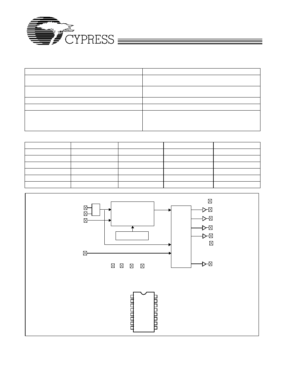
Frequency Table for CLKA-D
Part Number
CLKSEL=0
CLKSEL=1
Spread%
Parallel Crystal Load
CY26121
66.66 MHz
33.33
≠2.8%
6 pF
CY26121-2
33.33 MHz
25.00
≠2.8%
6 pF
CY26121-3
66.66 MHz
33.33
≠1.4%
6 pF
CY26121-11
66.66 MHz
33.33
≠2.8%
15 pF
CY26121-21
33.33 MHz
25.00
≠2.8%
15 pF
CY26121-31
66.66 MHz
33.33
≠1.4%
15 pF
16-pin TSSOP
CY26121
25 MHz XIN
XOUT
CLKA
OUTPUT
MULTIPLEXER
AND
DIVIDERS
OSC.
CLKC
VDDL
AVSS
AVDD
VSS
CLKB
REF
VSSL
VDD
CLKD
PLL
with
Modulation Control
Flash Configuration
SSON
CLKSEL
Logic Block Diagram
Pin Configuration
1
2
3
4
5
6
7
8
9
10
VDD
VSSL
CLKA
XOUT
NC
REF
VSS
CLKD
VDDL
SSON
CLKC
11
12
13
14
15
16
XIN
CLKB
AVSS
AVDD
CLKSEL
CY26121
Document #: 38-07350 Rev. **
Page 2 of 6
Absolute Maximum Conditions
Supply Voltage (V
DD
, AV
DD
, V
DDL
) ...................≠0.5 to +7.0V
DC Input Voltage ...................................... ≠0.5V to V
DD
+ 0.5
Storage Temperature
(Non-condensing) ....................................... ≠55
∞
C to +125
∞
C
Junction Temperature ................................ ≠40
∞
C to +125
∞
C
Data Retention @ Tj = 125
∞
C................................> 10 years
Package Power Dissipation...................................... 350 mW
Static Discharge Voltage.......................................... > 2000V
(per MIL-STD-883, Method 3015)
(Above which the useful life may be impaired. For user guide-
lines, not tested.)
Pin Description
Name
Pin Number
Description
XIN
1
Reference input or crystal input
VDD
2
3.3V voltage supply
AVDD
3
3.3V analog voltage
CLKSEL
4 (orig., -11,-3,-31)
0 = 66.66MHz out, 1 = 33.33 MHz out. Weak pull-up.
CLKSEL
4 (-2, -21)
0 = 33.33MHz out, 1 = 25 MHz out. Weak pull-up.
AVSS
5
Analog ground
VSSL
6
CLK ground
CLK(A:D)
7,8,9,12
Clock outputs at V
DDL
level
SSON
10
Spread Spectrum enable pin 0 = SS off; 1 = SS on. Weak pull-up.
VDDL
11
3.3V clock voltage supply
VSS
13
Ground
REF
14
Reference output at V
DD
level
NC
15
No Connect
XOUT
[1]
16
Crystal Output
Recommended Operating Conditions
Parameter
Description
Min.
Typ.
Max.
Unit
V
DD,
AV
DD
Supply voltage
3.135
3.30
3.465
V
V
DDL
Supply voltage for CLK (A-D)
3.135
3.30
3.465
V
T
A
Ambient temperature (commercial temp. grade)
0
70
∞ C
T
A
Ambient Temperature (industrial temp grade)
-40
85
∞ C
C
LOAD
Max. output load capacitance
15
pF
F
ref
Reference frequency
25
MHz
Crystal Specification
[2]
Parameter
Name
Min.
Typ
Max.
Unit
CR
load
Crystal load capacitance (original, -2, -3)
6
pF
CR
load
Crystal load capacitance (-11,-21,-31)
15
pF
ESR
Equivalent series resistance
50
Notes:
1.
Float XOUT if XIN is externally driven.
2.
A fundamental parallel resonant crystal must be used
CY26121
Document #: 38-07350 Rev. **
Page 3 of 6
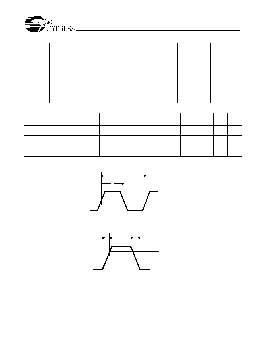
Voltage and Timing Definitions
Notes:
3.
Guaranteed by Characterization, not 100% tested.
DC Electrical Specifications
Parameter
Description
Condition
Min.
Typ.
Max.
Unit
I
OH
Output High Current
V
OH
= V
DD
≠ 0.5, V
DD
/V
DDL
=3.3V
12
24
mA
I
OL
Output Low Current
V
OL
= 0.5, V
DD
/V
DDL
= 3.3V
12
24
mA
I
IH
Input High Current
V
IH
= V
DD
5
10
µ
A
I
IL
Input Low Current
V
IL
= 0V
50
µ
A
V
IH
Input High Voltage
CMOS levels
0.7
V
DD
V
IL
Input Low Voltage
CMOS levels
0.3
V
DD
C
IN
[3]
Input Capacitance
Input pins excluding XIN
7
pF
R
UP
[3]
Pull-up resistor on input pins
V
DD
= 3.14 to 3.47V, measured at V
IN
= 0V
80
100
150
k
I
DD
Supply Current
AV
DD
/V
DD
/V
DDL
Current.
42
60
mA
AC Electrical Specifications
[3]
Parameter
Description
Condition
Min.
Typ.
Max.
Unit
DC
Output Duty Cycle
Duty Cycle is defined in Figure 1, 50% of V
DD
45
50
55
%
ER
Rising Edge Rate
Output Clock Edge Rate, Measured from 20%
to 80% of V
DD
, C
LOAD
= 15 pF See Figure 2.
0.8
1.4
V/ns
EF
Falling Edge Rate
Output Clock Edge Rate, Measured from 80%
to 20% of V
DD
, C
LOAD
= 15 pF See Figure 2.
0.8
1.4
V/ns
tj
RMS Clock Cycle-to-Cycle
Jitter
RMS cycle-to-cycle jitter with Spread on.
Measured at V
DD
/2.
15
40
ps
Clock
Output
V
DD
50% of V
DD
0V
t
1
t
2
Figure 1. Duty Cycle Definition
Clock
Output
t
3
t
4
V
DD
80% of V
DD
20% of V
DD
0V
Figure 2. ER = (0.6 x V
DD
) /t3, EF = (0.6 x V
DD
) /t4
CY26121
Document #: 38-07350 Rev. **
Page 4 of 6
Ordering Information
Ordering Code
Package Type
Operating Range
CY26121ZC
16-pin TSSOP
Commercial, 0∞C to 70∞C
CY26121ZCT
16-pin TSSOP ≠ Tape and Reel
Commercial, 0∞C to 70∞C
CY26121ZI
16-pin TSSOP
Industrial, ≠40∞C to 85∞C
CY26121ZIT
16-pin TSSOP ≠ Tape and Reel
Industrial, ≠40∞C to 85∞C
CY26121ZC-2
16-pin TSSOP
Commercial, 0∞C to 70∞C
CY26121ZC-2T
16-pin TSSOP ≠ Tape and Reel
Commercial, 0∞C to 70∞C
CY26121ZI-2
16-pin TSSOP
Industrial, ≠40∞C to 85∞C
CY26121ZI-2T
16-pin TSSOP ≠ Tape and Reel
Industrial, ≠40∞C to 85∞C
CY26121ZC-3
16-pin TSSOP
Commercial, 0∞C to 70∞C
CY26121ZC-3T
16-pin TSSOP ≠ Tape and Reel
Commercial, 0∞C to 70∞C
CY26121ZI-3
16-pin TSSOP
Industrial, ≠40∞C to 85∞C
CY26121ZI-3T
16-pin TSSOP ≠ Tape and Reel
Industrial, ≠40∞C to 85∞C
CY26121ZC-11
16-pin TSSOP
Commercial, 0∞C to 70∞C
CY26121ZC-11T
16-pin TSSOP ≠ Tape and Reel
Commercial, 0∞C to 70∞C
CY26121ZI-11
16-pin TSSOP
Industrial, ≠40∞C to 85∞C
CY26121ZI-11T
16-pin TSSOP ≠ Tape and Reel
Industrial, ≠40∞C to 85∞C
CY26121ZC-21
16-pin TSSOP
Commercial, 0∞C to 70∞C
CY26121ZC-21T
16-pin TSSOP ≠ Tape and Reel
Commercial, 0∞C to 70∞C
CY26121ZI-21
16-pin TSSOP
Industrial, ≠40∞C to 85∞C
CY26121ZI-21T
16-pin TSSOP ≠ Tape and Reel
Industrial, ≠40∞C to 85∞C
CY26121ZC-31
16-pin TSSOP
Commercial, 0∞C to 70∞C
CY26121ZC-31T
16-pin TSSOP ≠ Tape and Reel
Commercial, 0∞C to 70∞C
CY26121ZI-31
16-pin TSSOP
Industrial, ≠40∞C to 85∞C
CY26121ZI-31T
16-pin TSSOP ≠ Tape and Reel
Industrial, ≠40∞C to 85∞C
CY26121
Document #: 38-07350 Rev. **
Page 5 of 6
© Cypress Semiconductor Corporation, 2003. The information contained herein is subject to change without notice. Cypress Semiconductor Corporation assumes no responsibility for the use
of any circuitry other than circuitry embodied in a Cypress Semiconductor product. Nor does it convey or imply any license under patent or other rights. Cypress Semiconductor does not authorize
its products for use as critical components in life-support systems where a malfunction or failure may reasonably be expected to result in significant injury to the user. The inclusion of Cypress
Semiconductor products in life-support systems application implies that the manufacturer assumes all risk of such use and in doing so indemnifies Cypress Semiconductor against all charges.
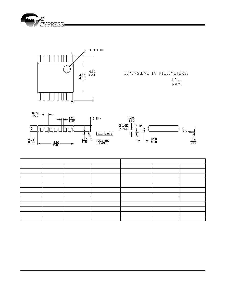
Package Drawing and Dimensions
All product and company names mentioned in this document are the trademarks of their respective holders.
16-lead Thin Shrunk Small Outline Package (4.40 MM Body) Z16
51-85091-**
Parameter
Inches
Millimeters
Min.
Nom.
Max.
Min.
Nom.
Max.
A
≠
≠
0.047
≠
≠
1.20
A
1
0.002
≠
0.006
0.05
≠
0.15
A2
0.031
0.039
0.041
0.80
1.00
1.05
B
0.007
≠
0.012
0.19
≠
0.30
C
0.004
≠
0.008
0.09
≠
0.20
D
0.193
0.197
0.201
4.90
5.00
5.10
E
0.169
0.173
0.177
4.30
4.40
4.50
e
0.026 BSC
0.65 BSC
H
0.244
0.252
0.260
6.20
6.40
6.60
L
0.018
0.024
0.030
0.45
0.60
0.75
a
0∞
≠
8∞
0∞
≠
8∞

CY26121
Document #: 38-07350 Rev. **
Page 6 of 6
Document History Page
Document Title: CY26121 PacketClockTM Spread Spectrum Clock Generator
Document Number: 38-07350
REV.
ECN NO.
Issue
Date
Orig. of
Change
Description of Change
**
121669
02/11/03
CKN
New Data Sheet