PRELIMINARY
Broadcom Reference Design
Clock Generator
CY26187-2
Cypress Semiconductor Corporation
∑
3901 North First Street
∑
San Jose
∑
CA 95134
∑
408-943-2600
Document #: 38-07131 Rev. *A
Revised December 14, 2002
5
Features
Benefits
∑ Integrated phase-locked loop
Highest Performance PLL tailored for multimedia applications
∑ Low skew, low jitter, high accuracy outputs
Meets critical timing requirements in complex system designs
∑ 3.3V Operation
Part Number
Outputs
Broadcom Reference
Design
Input Frequency
Output Frequencies
CY26187-2
1
BCM5680_5404
50 MHz
1 copy of 142.8 MHz (3.3V)
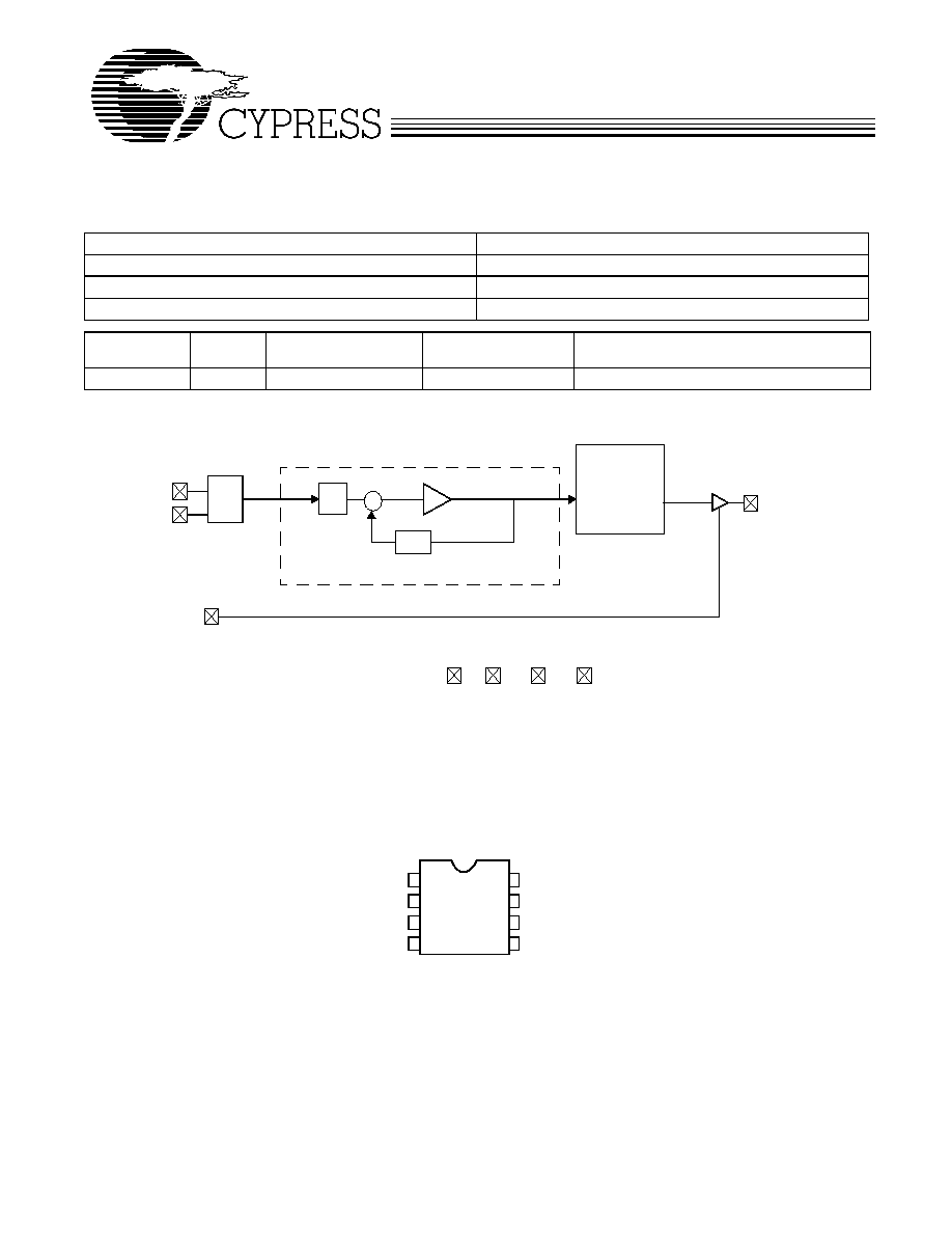
Logic Block Diagram
8-pin SOIC
CY26187
1
2
3
4
XOUT
XIN
AVSS
142.8 MHz
VDD
5
6
7
8
AVDD
OE
VSS
Pin Configuration
50 XIN
XOUT
OUTPUT
MULTIPLEXER
AND
DIVIDERS
PLL
OSC
Q
P
VCO
VDD
VSS
P Comp
VDD
VSS
142.8 MHz
OE
CY26187-2
PRELIMINARY
Document #: 38-07131 Rev. *A
Page 2 of 5
Absolute Maximum Conditions
Recommended Operating Conditions
DC Electrical Characteristics
Summary
Name
Pin Number
Description
XIN
[1]
1
Reference Crystal Input
AVDD
2
Analog Voltage Supply
OE
3
Output enable (0-off; 1-on)
AVSS
4
Ground
VDD
5
Voltage Supply
142.8 MHz
6
142.8-MHz clock output
VSS
7
Ground
XOUT
[1]
8
Reference Crystal Output
Parameter
Description
Min.
Max.
Unit
V
DD
Supply Voltage
7.0
V
T
S
Storage Temperature
[2]
≠65
125
∞C
T
J
Junction Temperature
125
∞C
Digital Inputs
V
SS
≠ 0.3
V
DD
+ 0.3
V
Digital Outputs referred to V
DD
V
SS
≠ 0.3
V
DD
+ 0.3
V
Electro-Static Discharge
2
kV
Parameter
Description
Min.
Typ.
Max.
Unit
V
DD
Operating Voltage
3.135
3.3
3.465
V
T
A
Ambient Temperature
0
70
C
C
LOAD
Max. Load Capacitance
15
pF
P
max
Max. Output Power Dissipation,
8-pin package
150
mW
f
REF
Reference Frequency
50
MHz
t
PU
Power-up time for all VDD's to
reach minimum specified voltage
(power ramps must be monotonic)
0.05
500
ms
Parameter
Name
Description
Min.
Typ.
Max.
Unit
Output High Current
V
OH
= V
DD
≠ 0.5, V
DD
= 3.3V
12
24
mA
Output Low Current
V
OL
= 0.5, V
DD
= 3.3V
12
24
mA
Input Capacitance
7
pF
Input Leakage Current
5
µ
A
I
VDD
3.3V, All outputs @ 10 MHz
35
mA
Notes:
1.
Float XOUT pin if XIN is driven by reference clock (as opposed to crystal).
2.
Rated for 10 years.
CY26187-2
PRELIMINARY
Document #: 38-07131 Rev. *A
Page 3 of 5
AC Electrical
Characteristics
(VDD = 3.3V)
(3.)
Note:
3.
Not 100% tested.
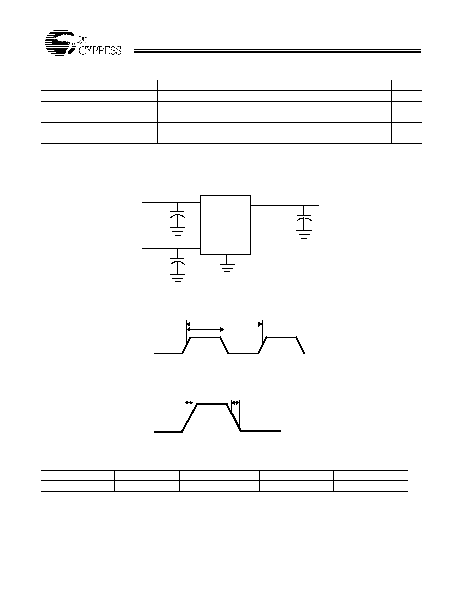
Figure 1. Duty Cycle Definition; DC = t2/t1.
Figure 2. Rise and Fall Time Definitions.
Parameter
Name
Description
Min.
Typ.
Max.
Unit
Output Duty Cycle
Duty Cycle is defined in Figure 1, 50% of V
DD
45
50
55
%
t3
Rising Edge Slew Rate Output Clock Rise Time, 20%-80% of V
DD
0.8
1.4
V/ns
t4
Falling Edge Slew Rate Output Clock Fall Time, 80% to 20% of V
DD
0.8
1.4
V/ns
t9
Clock Jitter
Peak to Peak period jitter
200
ps
t10
PLL Lock Time
3
ms
Test Circuit
Ordering Information
Ordering Code
Package Name
Package Type
Operating Range
Operating Voltage
CY26187SC-2
S8
8-Pin SOIC
Commercial
3.3V
0.1
µ
F
V
DD
0.1
µ
F
V
DD
CLK out
C
LOAD
GND
OUTPUTS
t1
t2
CLK
50%
t3
CLK
80%
20%
t4
CY26187-2
PRELIMINARY
Document #: 38-07131 Rev. *A
Page 4 of 5
© Cypress Semiconductor Corporation, 2001. The information contained herein is subject to change without notice. Cypress Semiconductor Corporation assumes no responsibility for the use
of any circuitry other than circuitry embodied in a Cypress Semiconductor product. Nor does it convey or imply any license under patent or other rights. Cypress Semiconductor does not authorize
its products for use as critical components in life-support systems where a malfunction or failure may reasonably be expected to result in significant injury to the user. The inclusion of Cypress
Semiconductor products in life-support systems application implies that the manufacturer assumes all risk of such use and in doing so indemnifies Cypress Semiconductor against all charges.
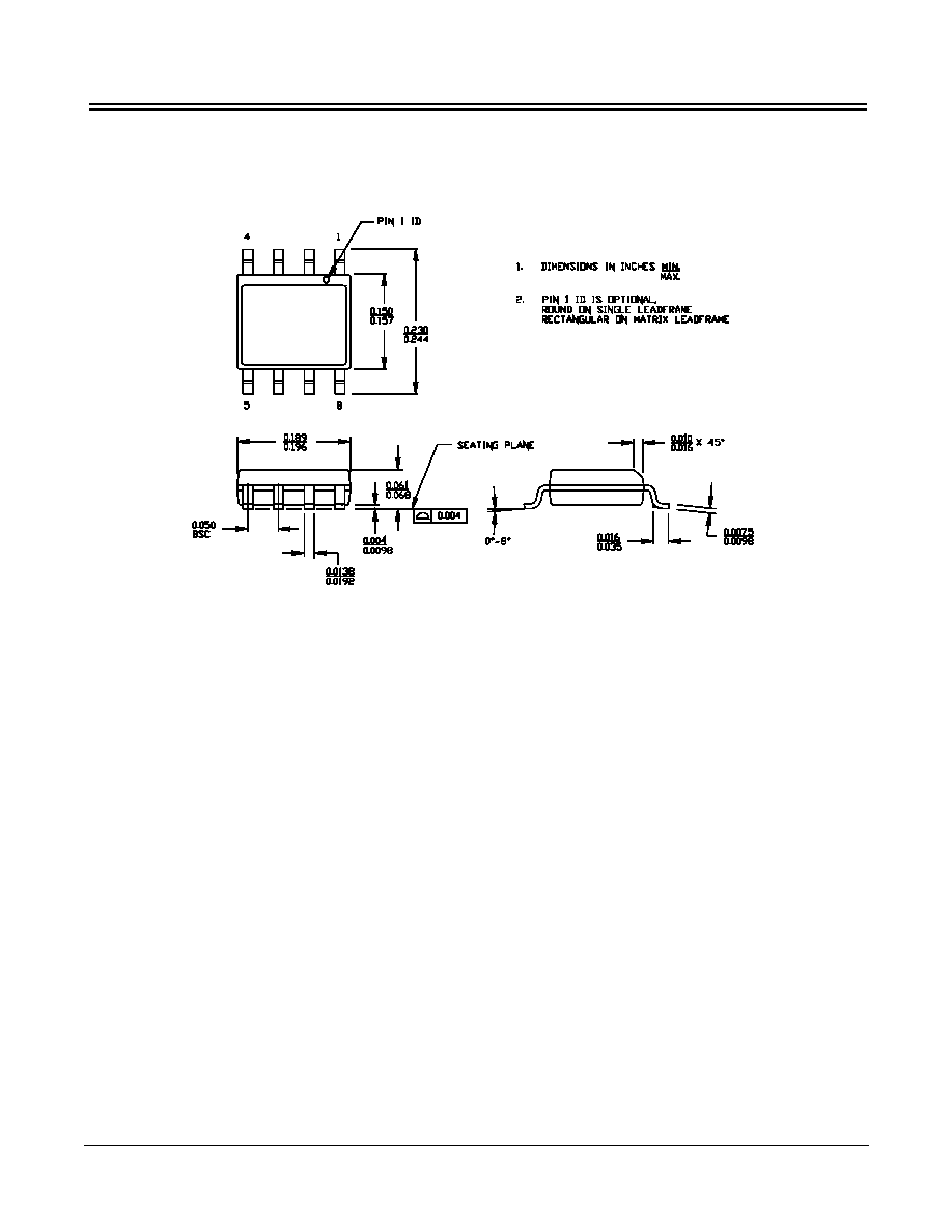
Package Diagram
8-Lead (150-Mil) SOIC S8
51-85066-A

CY26187-2
PRELIMINARY
Document #: 38-07131 Rev. *A
Page 5 of 5
Revision History
Document Title: CY26187-2 Broadcom Reference Design Clock Generator
Document Number: 38-07131
REV.
ECN NO.
Issue
Date
Orig. of
Change
Description of Change
**
110096
02/19/02
CKN
New data sheet
*A
121872
12/14/02
RBI
Power up requirements added to Operating Conditions Information