 | –≠–ª–µ–∫—Ç—Ä–æ–Ω–Ω—ã–π –∫–æ–º–ø–æ–Ω–µ–Ω—Ç: CY26211 | –°–∫–∞—á–∞—Ç—å:  PDF PDF  ZIP ZIP |
PacketClockTM
T1/E1 Clock Generator
CY26211
PRELIMINARY
Cypress Semiconductor Corporation
∑
3901 North First Street
∑
San Jose, CA 95134
∑
408-943-2600
Document #: 38-07447 Rev. **
Revised December 9, 2002
Features
Benefits
∑ Integrated phase-locked loop
High performance PLL tailored for T1/E1 clock generation
∑ Low jitter, high accuracy outputs
Meets critical timing requirements in complex system designs
∑ 3.3V Operation
Enables application compatibility
Part Number
Outputs
Input Frequency Range
Output Frequencies
CY26211
2
1.544 or 2.048 MHz
19.44 MHz, 77.76 MHz
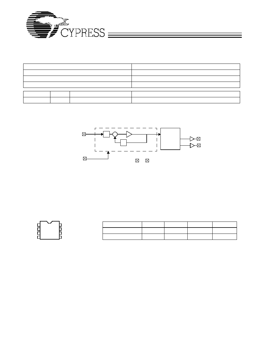
Logic Block Diagram
Fref
OUTPUT
DIVIDERS
PLL
Q
P
VCO
VDD
VSS
CLK1
8-pin SOIC
CY26211
Pin Configuration
1
2
3
4
NC
Fref
FS
CLK2
VSS
NC
CLK1
5
6
7
8
VDD
Table 1. CY26211 Frequency Select Option
Frequency Select
Fref
CLK1
CLK2
Unit
0
1.544
19.44
77.76
MHz
1
2.048
19.44
77.76
MHz
FS
CLK2
CY26211
Document #: 38-07447 Rev. **
Page 2 of 5
Pin Description
Name
Pin Number Description
Fref
1
1.544-MHz/2.048-MHz Reference Input
VDD
2
Voltage Supply
FS
3
Frequency Select. Weak internal pull-up. See Table 1 for a description of pin function.
VSS
4
Ground
CLK2
5
77.76-MHz Clock Output
CLK1
6
19.44-MHz Clock Output
NC
7
No Connect
NC
8
No Connect
Absolute Maximum Conditions
Parameter
Description
Min
Max
Unit
V
DD
Supply Voltage
≠0.5
7.0
V
T
S
Storage Temperature
[1]
≠65
125
∞C
T
J
Junction Temperature
125
∞C
Digital Inputs
V
SS
≠ 0.3
V
DD
+ 0.3
V
Digital Outputs referred to V
DD
V
SS
≠ 0.3
V
DD
+ 0.3
V
Electro-Static Discharge
2000
V
Recommended Operating Conditions
Parameter
Description
Min
Typ
Max
Unit
V
DD
Operating Voltage
3.135
3.3
3.465
V
T
A
Ambient Temperature (Commercial)
0
70
∞ C
C
LOAD
Max. Load Capacitance
15
pF
f
REF
Reference Frequency
1.544
2.048
MHz
DC Electrical Specifications (Commercial)
Parameter
Name
Description
Min
Typ
Max
Unit
I
OH
Output High Current
V
OH
= V
DD
≠ 0.5, V
DD
= 3.3V
12
24
mA
I
OL
Output Low Current
V
OL
= 0.5, V
DD
= 3.3V
12
24
mA
C
IN
Input Capacitance
7
pF
I
IH
Input Low Current
V
IL
= 0V
50
µ
A
I
IL
Input High Current
V
IH
= V
DD
5
µ
A
I
DD
Supply Current
Sum of Core and Output Current
20
mA
V
IH
Input High Voltage
CMOS levels, 70% of V
DD
0.7V
DD
V
V
IL
Input Low Voltage
CMOS levels, 30% of V
DD
0.3V
DD
V
R
UP
Pull-up resistor
V
DD
=3.14V to 3.47V, measured at V
IN
= 0V
100
150
k
AC Electrical Specifications
(V
DD
= 3.3V)
Parameter
[2]
Name
Description
Min
Typ
Max
Unit
DC
Output Duty Cycle
Duty Cycle is defined in Figure 1, 50% of V
DD
45
50
55
%
ERO
Rising Edge Rate
Output Clock Edge Rate, Measured from 20%
to 80% of V
DD
, C
LOAD
= 15pF See Figure 2.
0.8
1.4
V/ns
EFO
Falling Edge Rate
Output Clock Edge Rate, Measured from 80%
to 20% of V
DD
, C
LOAD
= 15pF See Figure 2.
0.8
1.4
V/ns
t
9
Clock Jitter
Peak to Peak Period Jitter
200
ps
t
10
PLL Lock Time
3
ms
Notes:
1.
Rated for 10 years
2.
Not 100% tested
CY26211
Document #: 38-07447 Rev. **
Page 3 of 5
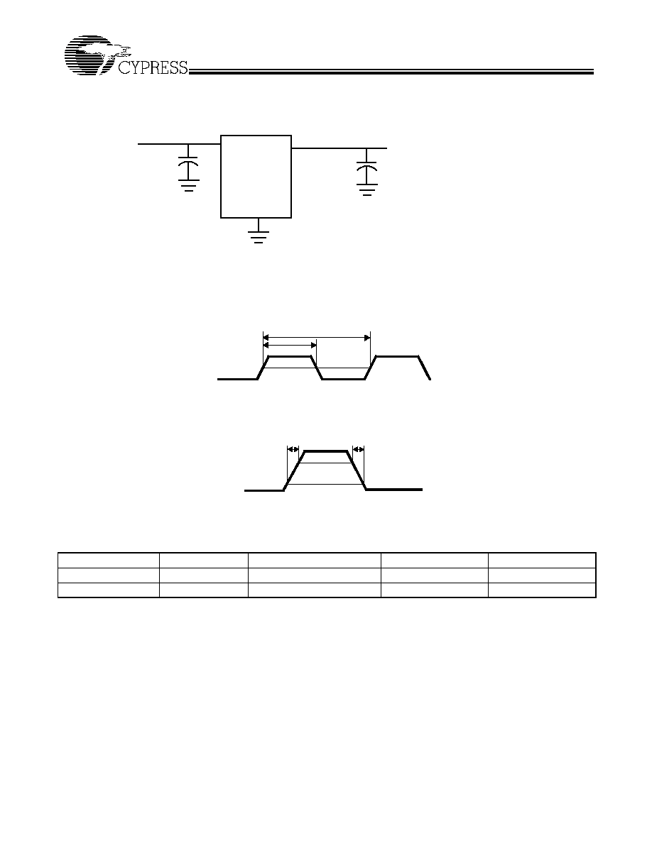
Voltage and Timing Definitions
Figure 1. Duty Cycle Definition; DC = t2/t1
Figure 2. Rise and Fall Time Definitions: ER = 0.6 x V
DD
/ t3, EF = 0.6 x V
DD
/ t4
Ordering Information
Test and Measurement Set-up
Ordering Code
Package Name
Package Type
Operating Range
Operating Voltage
CY26211SC
S8
8-Pin SOIC
Commercial
3.3V
CY26211SCT
S8
8-Pin SOIC - Tape and Reel
Commercial
3.3V
0.1
µ
F
V
DD
CLK out
C
LOAD
GND
OUTPUTS
t1
t2
CLK
50%
50%
t3
CLK
80%
20%
t4
CY26211
PRELIMINARY
Document #: 38-07447 Rev. **
Page 4 of 5
© Cypress Semiconductor Corporation, 2002. The information contained herein is subject to change without notice. Cypress Semiconductor Corporation assumes no responsibility for the use
of any circuitry other than circuitry embodied in a Cypress Semiconductor product. Nor does it convey or imply any license under patent or other rights. Cypress Semiconductor does not authorize
its products for use as critical components in life-support systems where a malfunction or failure may reasonably be expected to result in significant injury to the user. The inclusion of Cypress
Semiconductor products in life-support systems application implies that the manufacturer assumes all risk of such use and in doing so indemnifies Cypress Semiconductor against all charges.
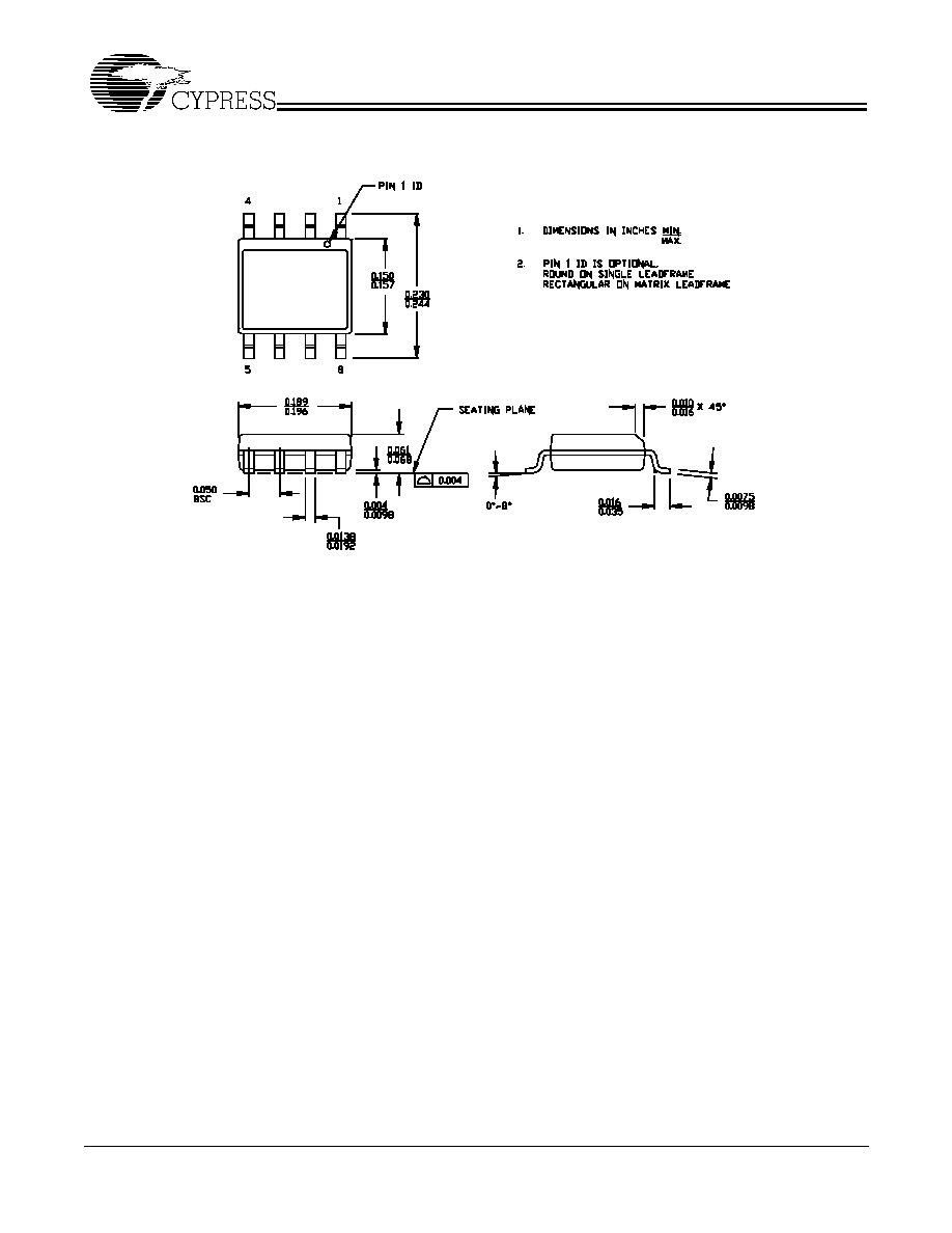
Package Drawing and Dimensions
All product or company names mentioned in this document may be the trademarks of their respective holders.
8-Lead (150-Mil) SOIC S8
51-85066-*A

CY26211
Document #: 38-07447 Rev. **
Page 5 of 5
Document History Page
Document Title: CY26211 PacketClockTM T1/E1 Clock Generator
Document Number: 38-07447
REV.
ECN NO.
Issue
Date
Orig. of
Change
Description of Change
**
121428
12/10/02
CKN
New data sheet