1
Selection Guide
27C128-45 27C128-55 27C128-70 27C128-90 27C128-120 27C128-150 27C128-200
Maximum Access Time (ns)
45
55
70
90
120
150
200
Maximum
Operating
Com'l
45
45
45
45
45
45
45
Operating
Current (mA)
[2]
Mil
55
55
55
55
55
55
55
Standby Current
( A)
Com'l
15
15
15
15
15
15
15
Standby Current
(mA)
Mil
20
20
20
20
20
20
20
Chip Select Time (ns)
45
55
70
90
120
150
200
Output Enable Time (ns)
15
20
25
30
30
40
40
Notes:
1. For PLCC only: Pins 1 and 17 are common and tied to the die attach
pad. They must therefore be DU (don't use) for the PLCC package.
2. Add 2 mA/MHz for AC power component.
CY27C128
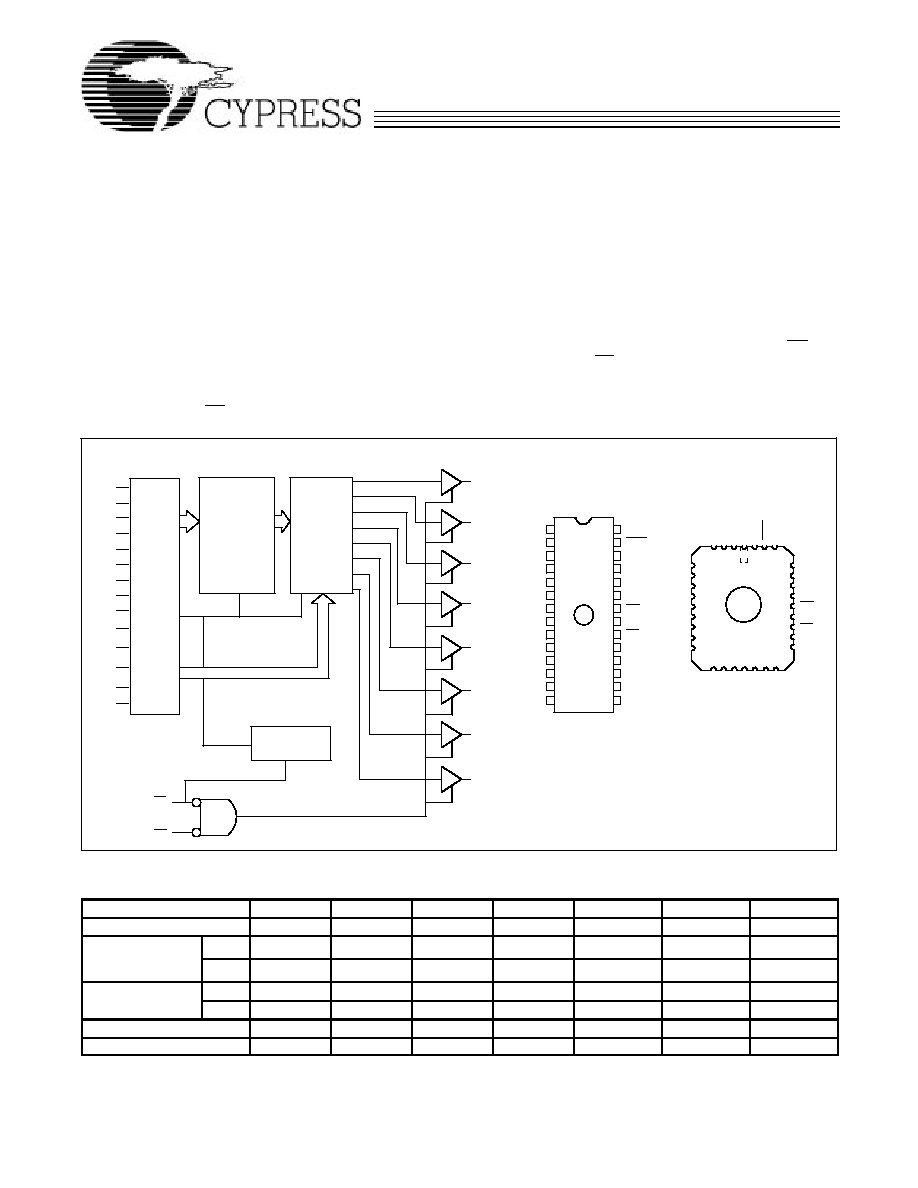
128K (16K x 8 Bit) CMOS EPROM
Features
D
Wide speed range
45 ns to 200 ns (commercial and
military)
D
Low power
248 mW (commercial)
303 mW (military)
D
Low standby power
Less than 83 mW when deselected
D
�10% Power supply tolerance
Functional Description
The CY27C128 is a high performance
16,384 word by 8 bit CMOS EPROM.
When disabled (CE HIGH), the
CY27C128 automatically powers down
into a low power stand by mode. The
CY27C128 is packaged in the industry
standard 600 mil DIP and LCC packages.
The CY27C128 is also available in a Cer
DIP package equipped with an erasure
window to provide for reprogrammability.
When exposed to UV light, the EPROM
is erased and can be reprogrammed. The
memory cells utilize proven EPROM
floating gate technology and byte wide in
telligent programming algorithms.
The CY27C128 offers the advantage of
lower power and superior performance and
programming yield. The EPROM cell re
quires only 12.5V for the super voltage,
and low current requirements allow for
gang programming. The EPROM cells al
low each memory location to be tested
100% because each location is written
into, erased, and repeatedly exercised
prior to encapsulation. Each EPROM is
also tested for AC performance to guar
antee that after customer programming,
the product will meet both DC and AC
specification limits.
Reading the CY27C128 is accomplished
by placing active LOW signals on OE and
CE. The contents of the memory location
addressed by the address lines (A
0
- A
13
)
will become available on the output lines
(O
0
- O
7
).
Logic Block Diagram
Pin Configurations
C128 1
A
12
A
11
A
9
A
8
A
7
A
6
A
5
A
4
A
3
A
2
A
1
A
0
POWER DOWN
O
7
O
6
O
5
O
4
O
3
O
2
O
1
O
0
CE
128 x 1024
PROGRAMABLE
ARRAY
8 x 1 OF 128
MULTIPLEXER
A
10
A
13
1
2
3
4
5
6
7
8
9
10
11
12
16
17
18
19
20
24
23
22
21
13
14
25
28
27
26
12
31
4
5
6
7
8
9
10
3 2 1
30
13
14 15 16 17
26
25
24
23
22
21
11
A
7
V CC
A
12
1819 20
27
28
29
32
15
DU
PGM A 13
A
12
A
7
A
6
A
5
A
4
A
3
A
2
A
1
A
0
O
0
O
1
O
2
GND
V
CC
A
13
A
8
A
9
O
7
O
6
O
4
O
5
O
3
C128 2
C128 3
A
9
A
11
O
7
O
6
A
8
V
PP
PGM
27C128
A
11
OE
A
10
CE
NC
A
5
A
4
A
3
A
2
A
6
A
1
O
0
A
0
V PP
NC
OE
A
10
CE
O
4
GND
O
3
O
1
DU
O
5
O
2
DIP/Flatpack
27C128
ROW
LCC/PLCC
[1]
OE
ADDRESS
COLUMN
ADDRESS
ADDRESS
DECODER
Cypress Semiconductor Corporation
D
3901 North First Street
D
San Jose
D
CA 95134
D
408-943-2600
February 1994
CY27C128
2
Maximum Ratings
(Above which the useful life may be impaired. For user guidelines,
not tested.)
Storage Temperature
-65
_
C to +150
_
C
. . . . . . . . . . . . . . . . . .
Ambient Temperature with
Power Applied
-55
_
C to +125
_
C
. . . . . . . . . . . . . . . . . . . . . . .
Supply Voltage to Ground Potential
-0.5V to +7.0V
. . . . . . . .
DC Voltage Applied to Outputs
in High Z State
-0.5V to +7.0V
. . . . . . . . . . . . . . . . . . . . . . . . .
DC Input Voltage
-3.0V to +7.0V
. . . . . . . . . . . . . . . . . . . . . . .
DC Program Voltage
13.0V
. . . . . . . . . . . . . . . . . . . . . . . . . . . . .
Static Discharge Voltage
>2001V
. . . . . . . . . . . . . . . . . . . . . . . .
(per MIL STD 883, Method 3015)
Latch Up Current
>200 mA
. . . . . . . . . . . . . . . . . . . . . . . . . . .
UV Exposure
7258 Wsec/cm
2
. . . . . . . . . . . . . . . . . . . . . . . . . . .
Operating Range
Range
Ambient
Temperature
V
CC
Commercial
0
_
C to +70
_
C
5V �10%
Industrial
[3]
-40
_
C to +85
_
C
5V �10%
Military
[4]
-55
_
C to +125
_
C
5V �10%
Electrical Characteristics
Over the Operating Range
[5]
27C128-45, 55, 70, 90,
120, 150, 200
Parameter
Description
Test Conditions
Min.
Max.
Unit
V
OH
Output HIGH Voltage
V
CC
= Min., I
OH
= -4.0 mA
2.4
V
V
OL
Output LOW Voltage
V
CC
= Min., I
OL
= 16.0 mA
[6]
0.4
V
V
IH
Input HIGH Level
Guaranteed Input Logical HIGH Voltage for
All Inputs
2.0
V
CC
V
V
IL
Input LOW Level
Guaranteed Input Logical LOW Voltage for
All Inputs
-0.3
0.8
V
I
IX
Input Current
GND < V
IN
< V
CC
-10
+10
mA
I
OZ
Output Leakage Current
GND < V
OUT
< V
CC
,
Output Disabled
Commercial
-10
+10
mA
Output Disabled
Military
-40
+40
I
OS
Output Short Circuit Current
[7]
V
CC
= Max., V
OUT
= GND
-20
-90
mA
I
CC
Power Supply Current
[2]
V
CC
= Max., V
IN
=V
IH
,
I
OUT
= 0 mA, CE=V
IL
,
Commercial
45
mA
I
OUT
= 0 mA, CE=V
IL
,
OE = V
IH
Military
55
I
SB
Standby Supply Current
V
CC
= Max., CE = V
IH
Commercial
15
mA
Military
20
V
PP
Programming Supply Voltage
12
13
V
I
PP
Programming Supply Current
50
mA
V
IHP
Input HIGH Programming
Voltage
3.0
V
V
ILP
Input LOW Programming
Voltage
0.4
V
Capacitance
[8]
Parameter
Description
Test Conditions
Max.
Unit
C
IN
Input Capacitance
T
A
= 25
_
C, f = 1 MHz,
V
CC
= 5 0V
10
pF
C
OUT
Output Capacitance
A
V
CC
= 5.0V
10
pF
Notes:
3. Contact a Cypress representative for information on industrial tem
perature range specifications.
4. T
A
is the instant on" case temperature.
5. See the last page of this specification for Group A subgroup testing in
formation.
6 I
OL
=12.0 mA for military devices.
7. For test purposes, not more than one output at a time should be
shorted. Short circuit test duration should not exceed 30 seconds.
8. See Introduction to CMOS PROMs in this Data Book for general in
formation on testing.
CY27C128
3
AC Test Loads and Waveforms
C128 4
C128 5
90%
10%
3.0V
GND
90%
10%
ALL INPUT PULSES
5V
OUTPUT
30 pF
INCLUDING
JIG AND
SCOPE
5V
OUTPUT
5 pF
INCLUDING
JIG AND
SCOPE
(a) Normal Load
(b) High Z Load
< 5 ns
< 5 ns
OUTPUT
R1 250W (329W MIL)
R2 167W
(202W MIL
100W
Equivalent to:
TH�VENIN EQUIVALENT
2.00 V
R2 167W
(202W MIL
R1 250W (329W MIL)
OUTPUT
125W
1.9 V
Commercial
Military
Switching Characteristics
Over the Operating Range
[4, 7]
27C128-45
27C128-55
27C128-70
27C128-90
Parameter
Description
Min.
Max.
Min.
Max.
Min.
Max.
Min.
Max.
Unit
t
AA
Address to Output Valid
45
55
70
90
ns
t
HZOE
Outpout Enable Inactive to High Z
15
20
25
25
ns
t
OE
Output Enable Active to Output Valid
15
20
25
30
ns
t
HZCE
Chip Enable Inactive to High Z
20
25
25
25
ns
t
ACE
Chip Enable Active to Output Valid
45
55
70
90
ns
t
PU
Chip Enable Active to Power Up
0
0
0
0
ns
t
PD
Chip Enable Inactive to Power Down
45
55
70
90
ns
t
OH
Output Hold from Address Change
0
0
0
0
ns
Switching Characteristics
Over the Operating Range
[4, 7]
(continued)
27C128-120
27C128-150
27C128-200
Parameter
Description
Min.
Max.
Min.
Max.
Min.
Max.
Unit
t
AA
Address to Output Valid
120
150
200
ns
t
HZOE
Outpout Enable Inactive to High Z
30
30
30
ns
t
OE
Output Enable Active to Output Valid
30
40
40
ns
t
HZCE
Chip Enable Inactive to High Z
30
30
30
ns
t
ACE
Chip Enable Active to Output Valid
120
150
200
ns
t
PU
Chip Enable Active to Power Up
0
0
0
ns
t
PD
Chip Enable Inactive to Power Down
120
150
200
ns
t
OH
Output Hold from Address Change
0
0
0
ns
CY27C128
4
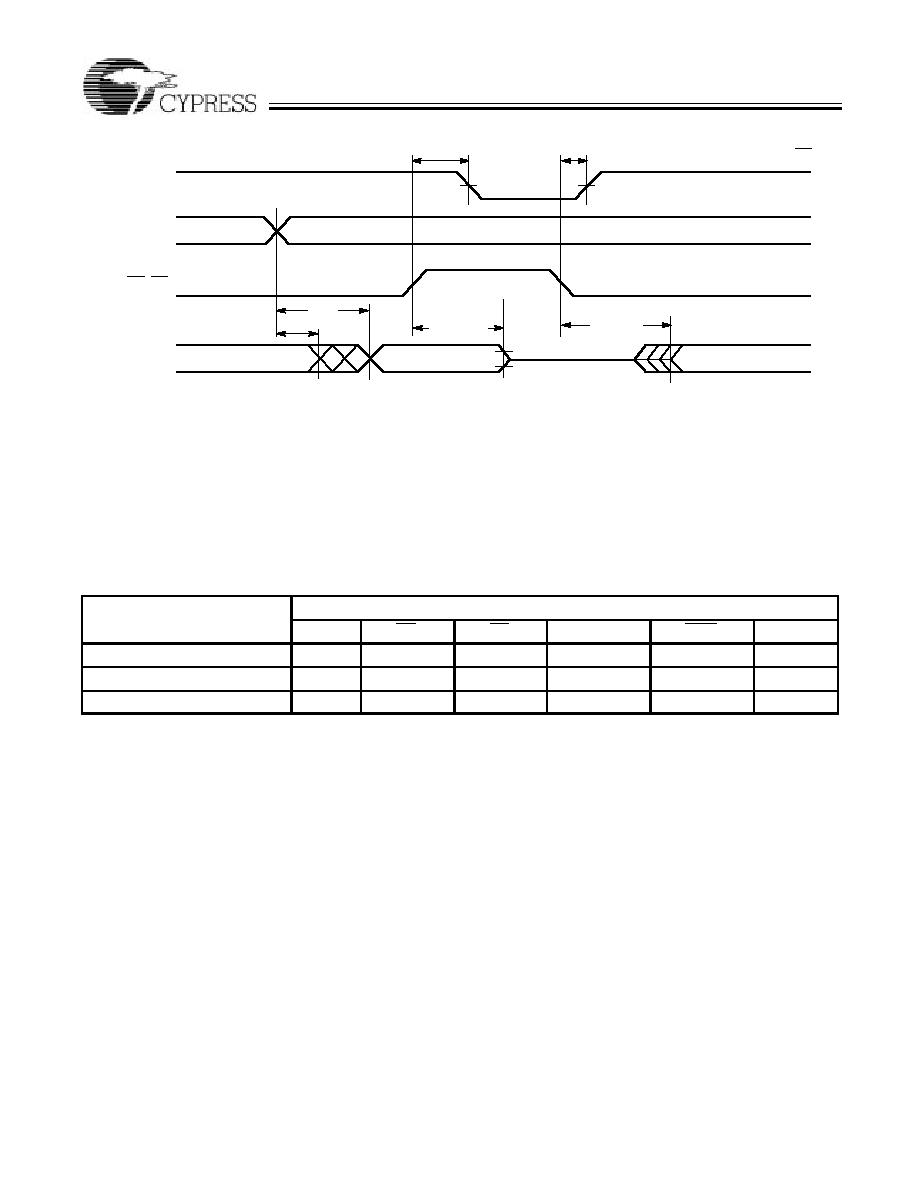
Switching Waveform
t
OH
t
PU
t
PD
t
AA
C128 6
(t
OE
)
t
ACE
50%
50%
A
0
- A
13
ADDRESS
I
CC
SUPPLY
CURRENT
OE, CE
O
0
- O
7
PREVIOUS DATA VALID
DATA VALID
POWER DOWN CONTROLLED BY CE
(t
HZOE
)
t
HZCE
HIGH Z
Erasure Characteristics
Wavelengths of light less than 4000 � begin to erase the 27C128
in the windowed package. For this reason, an opaque label should
be placed over the window if the EPROM is exposed to sunlight
or fluorescent lighting for extended periods of time.
The recommended dose of ultraviolet light for erasure is a wave
length of 2537 � for a minimum dose (UV intensity multiplied by
exposure time) of 25 Wsec/cm
2
. For an ultraviolet lamp with a 12
mW/cm
2
power rating, the exposure time would be approximately
35 minutes. The CY27C128 needs to be within 1 inch of the lamp
during erasure. Permanent damage may result if the EPROM is
exposed to high intensity UV light for an extended period of
time. 7258 Wsec/cm
2
is the recommended maximum dosage.
Programming Modes
Programming support is available from Cypress as well as from a
number of third party software vendors. For detailed program
ming information, including a listing of software packages, please
see the EPROM Programming Information located at the end of
this section. Programming algorithms can be obtained from any
Cypress representative.
Table 1. CY27C128 Mode Selection
Pin Function
[9]
Mode
A
13
- A
0
OE
CE
V
PP
PGM
O
7
- O
0
Read
A
13
- A
0
V
IL
V
IL
X
Note 10
O
7
- O
0
Output Disable
A
13
- A
0
V
IH
X
X
Note 10
High Z
Power Down
A
13
- A
0
X
V
IH
X
Note 10
High Z
Notes:
9. X must be either V
IL
or V
IH.
10. X must be either V
IL
or V
IH
(must not switch).
CY27C128
5
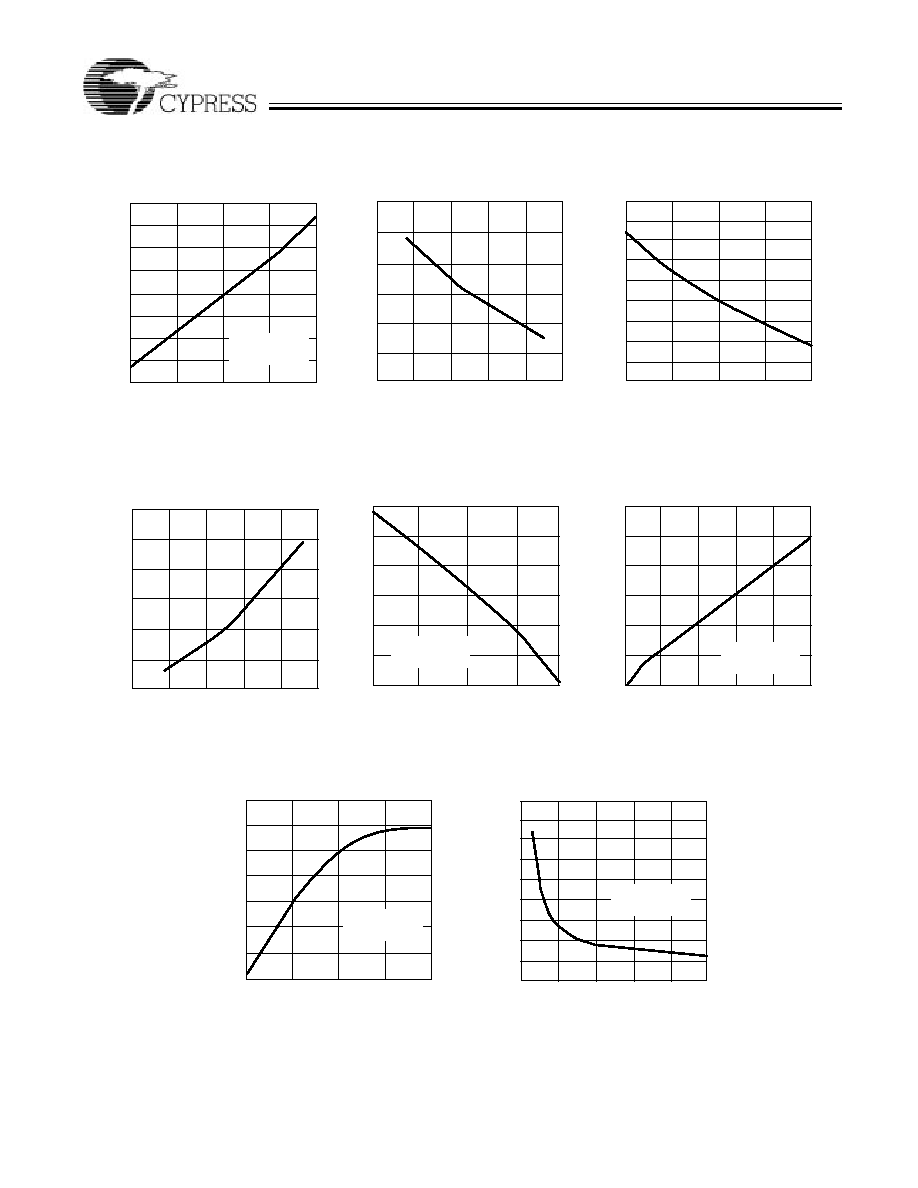
Typical DC and AC Characteristics
1.0
0.8
0.7
4.0
4.5
5.0
5.5
6.0
-100 -50
150
1.2
1.1
1.2
1.1
1.0
0.9
4.0
4.5
5.0
5.5
6.0
NORMALIZED ACCESS
TIME
SUPPLY VOLTAGE (V)
NORMALIZED SUPPLY CURRENT
vs. SUPPLY VOLTAGE
NORMALIZED SUPPLY CURRENT
vs. AMBIENT TEMPERATURE
AMBIENT TEMPERATURE (_C)
SUPPLY VOLTAGE (V)
NORMALIZED ACCESS TIME
vs. SUPPLY VOLTAGE
0.6
0.9
NORMALIZED ACCESS
TIME
AMBIENT TEMPERATURE (_C)
NORMALIZED ACCESS TIME
vs. TEMPERATURE
1.0
0.9
0.8
NORMALIZED I
CC
NORMALIZED I
CC
0.8
60
50
40
30
20
10
0
1.0
2.0
3.0
OUTPUT SOURCE CURRENT (mA)
OUTPUT VOLTAGE (V)
30.0
25.0
20.0
15.0
10.0
5.0
0
200
400
600
800
DEL
T
A t (ns)
AA
CAPACITANCE (pF)
TYPICAL ACCESS TIME CHANGE
vs. OUTPUT LOADING
4.0
0.0
1000
V
CC
= 4.5V
T
A
= 25_C
T
A
= 25_C
f = f
MAX
0
OUTPUT SOURCE CURRENT
vs. OUTPUT VOLTAGE
1.4
1.2
1.1
1.3
0.7
1.3
0
50
100
0.85
0.95
1.05
1.15
1.25
-100 -50
150
1.3
1.2
1.1
1.0
0.9
0.8
1.4
0
50
100
V
CC
= 5V
T
A
= 25_C
1.15
1.05
0.95
0.85
CYCLE TIME (ns)
NORMALIZEDSUPPLY CURRENT
vs. ACCESS TIME
0.75
0.8
0.9
1.0
1.1
1.2
NORMALIZED I
CC
0
100
200
300
400 500
V
CC
= 5.6V
T
A
= 25_C
150
175
125
75
50
25
0.0
1.0
2.0
3.0
OUTPUT SINK CURRENT (mA)
0
100
OUTPUT VOLTAGE (V)
OUTPUT SINK CURRENT
vs. OUTPUT VOLTAGE
V
CC
= 5.0V
T
A
= 25_C
4.0