1 PLL In-System Programmable Clock Generator
with Individual 16K EEPROM
CY27EE16ZE
Cypress Semiconductor Corporation
∑
3901 North First Street
∑
San Jose
,
CA 95134
∑
408-943-2600
Document #: 38-07440 Rev. *B
Revised June 30, 2003
Features
Benefits
∑ 18 kbits of EEPROM
16 kbits independent scratch
2 kbits dedicated to clocking functions
Higher level of integration and reduced component count by
combining EEPROM and PLL. Independent EEPROM may be used
for scratch memory, or to store up to eight clock configurations
∑ Integrated, phase-locked loop with programmable P
and Q counters, output dividers, and optional
analog VCXO, digital VCXO, spread spectrum for
EMI reduction
High-performance PLL enables control of output frequencies that are
customizable to support a wide range of applications
∑ In system programmable through I
2
C Serial
Programming Interface (SPI). Both the SRAM and
non-volatile EEPROM memory bits are program-
mable with the 3.3V supply
Familiar industry standard eases programming effort and enables
update of data stored in 16K EEPROM scratchpad and 2K EEPROM
clock control block while CY27EE16ZE is installed in system
∑ Low-jitter, high-accuracy outputs
Meets critical timing requirements in complex system designs
∑ VCXO with analog adjust
Write Protect (WP pin) can be programmed to serve as an analog
control voltage for a VCXO.The VCXO function is still available with
a DCXO, or digitally controlled (through SPI) crystal oscillator if the
pin is functioning as WP
∑ 3.3V Operation (optional 2.5V outputs)
Meets industry-standard voltage platforms
∑ 20-lead Exposed Pad, EP-TSSOP
Industry standard packaging saves on board space
Part Number
Outputs
Input Frequency Range
Output Frequency Range
CY27EE16ZE
6
1 ≠ 167 MHz (Driven Clock Input) {Commercial}
1 ≠150 MHz (Driven Clock Input) {Industrial}
8 ≠ 30 MHz (Crystal Reference) {Comm. or Ind.}
80 kHz ≠ 200 MHz (3.3V) {Commercial}
80 kHz ≠167 MHz (3.3V) {Industrial}
80 kHz ≠167 MHz (2.5V) {Commercial}
80 kHz ≠ 150 MHz (2.5V) {Industrial}
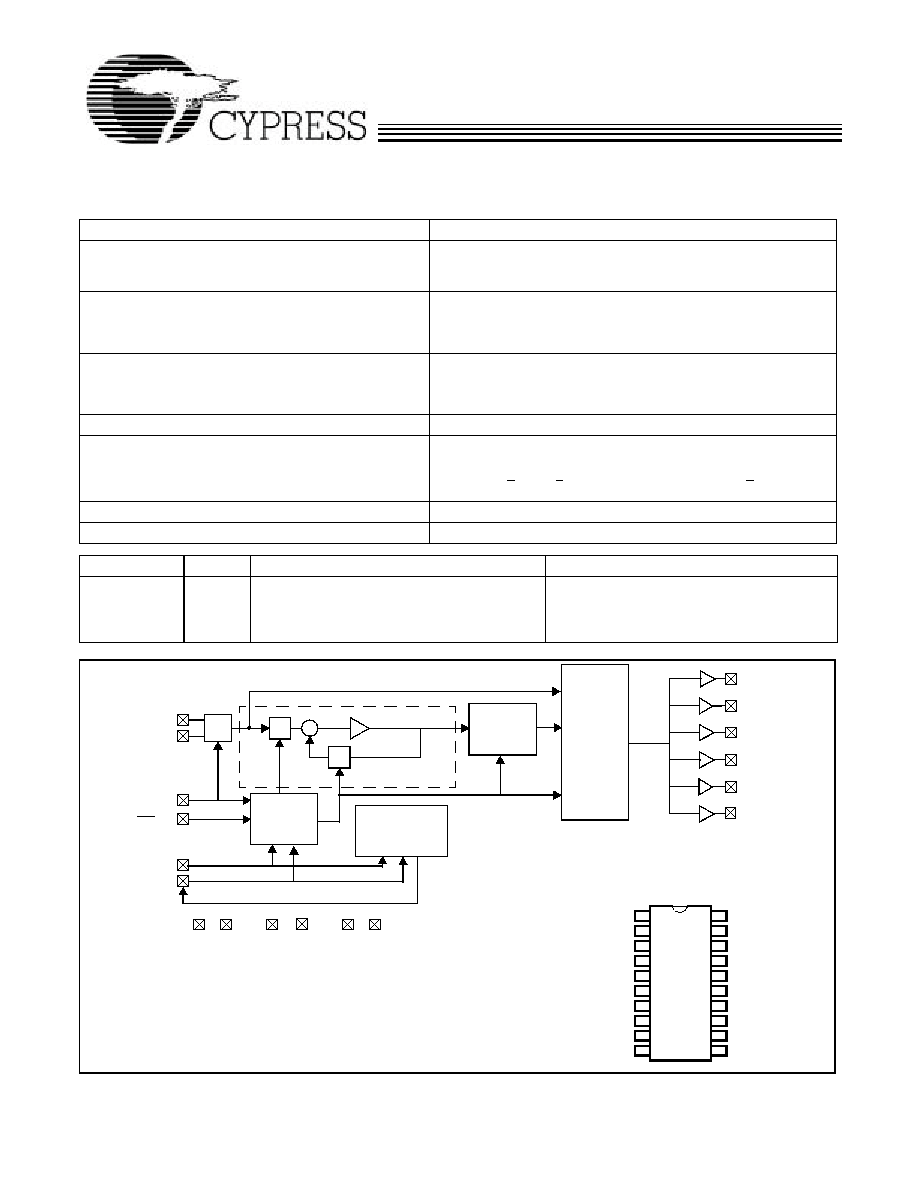
Logic Block Diagram
XIN
XOUT
CLOCK2
OUTPUT
DIVIDERS
PLL
OSC
CLOCK1
Q
VCO
VDD
VSS
CLOCK3
P
Pin Configurations
SCL
SDAT
8x2k EEPROM
Memory Array
Clock
Configuration
Output
Crosspoint
Switch
Array
CLOCK5
CLOCK4
CLOCK6
[I
2
C- SPI:]
20-pin EP-TSSOP
AVDD AVSS
VDDL
VSSL
CY27EE16ZE
PDM/OE
XIN 1
20 XOUT
VDD 2
19 VDD
CLOCK6 3
18 CLOCK5
AVDD 4
17 VCXO/WP
SDAT 5
16 VSS
AVSS 6
15 CLOCK4
VSSL 7
14 VDDL
CLOCK1 8
13 SCL
CLOCK2 9
12 CLOCK3
OE/PDM 10
11 VDDL
VCX/WP
CY27EE16ZE
Document #: 38-07440 Rev. *B
Page 2 of 17
Functional Description
The CY27EE16ZE integrates a 16-kbit EEPROM scratchpad
and a clock generator that features Cypress's programmable
clock core. An industry standard I
2
C serial programming
interface (SPI) is used to program the scratchpad and clock
core.
16-kbit EEPROM
The 16-kbit EEPROM scratchpad is organized in eight blocks
x 256 words x 8 bits. Each of the eight 2-kbit EEPROM
scratchpad blocks, a 2-kbit clock configuration EEPROM
block, and a 2-kbit volatile clock configuration SRAM block,
have their own 7-bit device address. The device address is
combined with a Read/Write bit as the LSB and is sent after
each start bit.
Clock Features
The programmable clock core is configured with the following
features:
∑ Crystal Oscillator: Programmable drive and load, support
for external references up to 166 MHz. See "Reference
Frequency (REF)", page 5
∑ VCXO: Analog or digital control
∑ Inputs and I/Os: Programmable input muxes drive write
protect (WP), analog VCXO control, output enable (OE),
and power down mode (PDM) functions
∑ PLL: Programmable P, Q, offset, and loop filter parameters.
Outputs: Six outputs and two programmable linear dividers.
The output swing of CLOCK1 through CLOCK4 is set by VDDL
(2.5V or 3.3V). The output swing of CLOCK5 and CLOCK6 is
set by VDD (3.3V).
Clock configuration is stored in a dedicated 2-kbit block of
nonvolatile EEPROM and a 2-kbit block of volatile SRAM. The
SPI is used to write new configuration data to the on-chip
programmable registers that are defined within the clock
configuration memory blocks. Other, custom configurations,
that include custom VCXO, Spread Spectrum for EMI
reduction, Fractional N and frequency select pins (FS) are
programmable; contact factory for details.
Write Protect (WP) ≠ Active HIGH
The default clock configuration of the CY27EE16ZE has pin
17 configured as WP. When a logical HIGH level input is
asserted on this pin, the write protect feature (WP) will inhibit
writing to the EEPROM. This protects EEPROM bits from
being changed, while allowing full read access to EEPROM.
Writing to SRAM is allowed with WP enabled. When this pin is
held at a logical LOW level, WP is disabled and data can be
written to EEPROM.
Analog Adjust for Voltage Controlled Crystal Oscillator
(VCXO)
Pin 17 can be programmed, with the SPI, to function as the
analog control for the VCXO. Then, pin 17 provides ±150 ppm
adjustment of the crystal oscillator frequency (in order to use
the VCXO, the crystal must have a minimum of ±150 ppm pull
range and meet the pullable crystal specifications as shown in
Table 15 on page 12). The crystal oscillator frequency is pulled
lower by at least 150 ppm when 0V is applied to VCXO, pulled
higher by at least 150 ppm when V
DD
is applied to VCXO. The
oscillator frequency will have a linear dependence on the
voltage level applied to pin 17, VCXO, within a range from 0V
to V
DD
. See section "Device Addressing", page 10 for more
information.
Note:
1.Float XOUT if XIN is externally driven.
Table 1. Pin Description
Name
Pin Number
Description
XIN
1
Reference crystal input
VDD
2, 19
3.3V voltage supply
CLOCK6
3
Clock output 6
AVDD
4
3.3V analog voltage supply
SDAT
5
Data input for serial programming
AVSS
6
Analog ground
VSSL
7
Output ground
CLOCK1
8
Clock output 1
CLOCK2
9
Clock output 2
OE/PDM
10
Output enable or power-down mode enable
VDDL
11,14
Output voltage supply
CLOCK3
12
Clock output 3
SCL
13
Clock signal input for serial programming
CLOCK4
15
Clock output 4
VSS
16
Ground
VCXO/WP
17
Analog control input for VCXO or write protect (user-configurable)
CLOCK5
18
Clock output 5
XOUT
[1]
20
Reference crystal output
CY27EE16ZE
Document #: 38-07440 Rev. *B
Page 3 of 17
Output Enable (OE) ≠ Active HIGH
The default clock configuration has pin 10 programmed as an
Output Enable (OE). This pin enables the divider bank clock
outputs when HIGH, and disables divider bank clock outputs
when LOW.
Power-down Mode (PDM) ≠ Active LOW
The Power-down Mode (PDM) function is available when pin
10 of the CY27EE16ZE is configured as PDM. When the PDM
signal pulled LOW, all clock components are shut down and
the part enters a low-power state. To configure pin 10 of the
CY27EE16ZE as PDM, see "Power-down Mode (PDM) and
Output Enable (OE) Registers for Pin 10", page 7.
Serial Programming Interface (SPI)
The SPI uses industry-standard signaling in both standard and
fast modes to program the 8 x 2 kbit EPPROM blocks of
scratchpad, the 2-kbit EEPROM dedicated to clock configu-
ration, and the 2-kbit SRAM block. See sections beginning
with "Using the Serial Programming Interface (SPI)", page 3
for more information.
Default Start-up Condition for CY27EE16ZE
The default (programmed) condition of the 8 x 256 bit
EEPROM blocks (scratchpad) in the device as shipped from
the factory, are blank and unprogrammed. In this condition, all
bits are set to 0.
The default clock configuration is:
∑the crystal oscillator circuit is active.
∑CLOCK1 outputs REF frequency.
∑All other outputs are three-stated.
∑WP control on pin 17.
∑OE control on pin 10.
This default clock configuration is typically customized to meet
the needs of a specific application. It provides a clock signal
upon power-on, to facilitate in-system programming. Alterna-
tively, the CY27EE16ZE may be programmed with a different
clock configuration prior to placement of the CY27EE16ZE in
systems. While you can develop your own subroutine to
program any or all of the individual registers described in the
following pages, it may be easier to use CyClocksRTTM to
produce the required register setting file.
Using the Serial Programming Interface (SPI)
The CY27EE16ZE provides an industry-standard serial
programming interface for volatile and nonvolatile, in-system
programming of unique frequencies and options. Serial
programming and reprogramming allows for quick design
changes and product enhancements, eliminates inventory of
old design parts, and simplifies manufacturing.
The CY27EE16ZE is a group of ten slave devices with
addresses as shown in Figure 1. The serial programming
interface address of the CY27EE16ZE clock configuration
2-kbit EEPROM block is 69H. The serial programming
interface address of the CY27EE16ZE clock configuration
2-kbit SRAM block is 68H. Should there be a conflict with any
other devices in your system, all device addresses can also be
changed using CyberClocks. Registers in the clock configu-
ration 2-kbit SRAM memory block are written, when the user
wants to update the clock configuration for on-the-fly changes
.
Registers in the clock configuration EEPROM block are
written, if the user wants to update the clock configuration so
that it is saved and used again after power-up or reset.
All programmable registers in the CY27EE16ZE are
addressed with eight bits and contain eight bits of data. Table 2
lists the specific register definitions and their allowable values.
See section "Serial Programming Interface Timing", page 12,
for a detailed description.
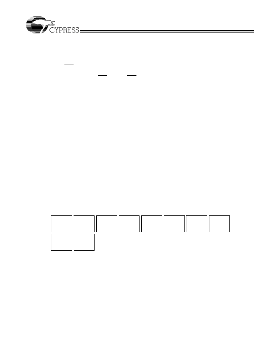
1st
EE block
256 x 8 bits
Address:
1000000
4th
EE block
256 x 8 bits
Address:
1000011
3rd
EE block
256 x 8 bits
Address:
1000010
2nd
EE block
256 x 8 bits
Address:
1000001
clock config.
EE block
256 x 8 bits
Address:
1101000
clock config.
SRAM
256 x 8 bits
Address:
1101001
5th
EE block
256 x 8 bits
Address:
1000100
8th
EE block
256 x 8 bits
Address:
1000111
7th
EE block
256 x 8 bits
Address:
1000110
6th
EE block
256 x 8 bits
Address:
1000101
Figure 1. Device Addresses for EEPROM Scratchpad and Clock Configuration Blocks
CY27EE16ZE
Document #: 38-07440 Rev. *B
Page 4 of 17
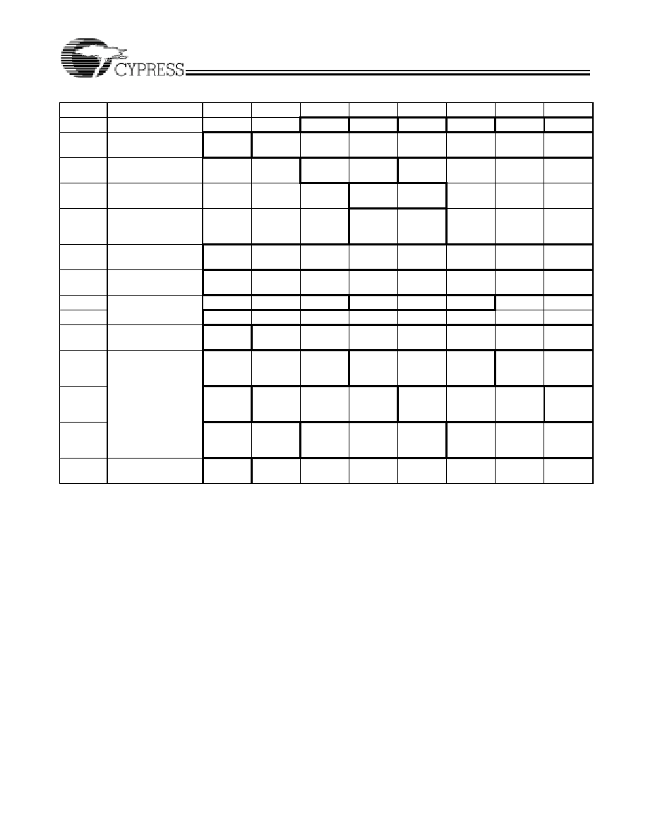
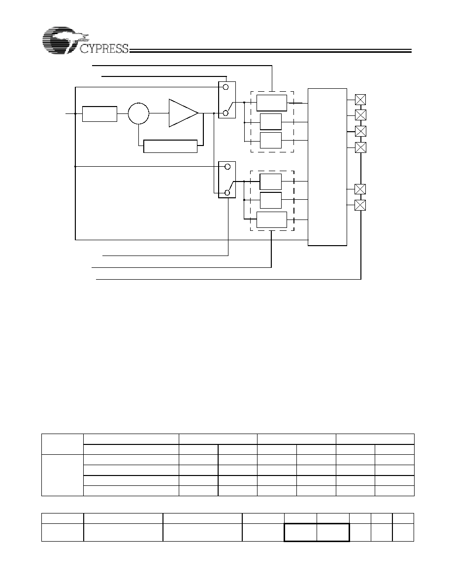
CY27EE16ZE Frequency Calculation and
Register Definitions
The CY27EE16ZE is an extremely flexible clock generator
with four basic variables that can be used to determine the final
output frequency. They are the input reference frequency
(REF), the internally calculated P and Q dividers, and the post
divider, which can be a fixed or calculated value. There are
three basic formulas for determining the final output frequency
of a CY27EE16ZE-based design. Any one of these three
formulas may be used:
CLK = ((REF * P)/Q)/Post Divider
CLK = REF/Post Divider
CLK = REF
The basic PLL block diagram is shown in Figure 2. Each of the
six clock outputs on the CY27EE16ZE has a total of seven
output options available to it. There are six post divider options
available: /2 (two of these), /3, /4, /DIV1N and /DIV2N. DIV1N
and DIV2N are independently calculated and are applied to
individual output groups. The post divider options can be
applied to the calculated VCO frequency ((REF*P)/Q) or to the
reference frequency directly.
In addition to the six post divider output options, the seventh
option bypasses the PLL and passes the reference frequency
directly to the crosspoint switch matrix.
Table 2. Summary Table ≠ CY27EE16ZE Programmable Registers
Register
Description
D7
D6
D5
D4
D3
D2
D1
D0
09H
CLKOE control
0
CLOCK6
CLOCK5
0
CLOCK4
CLOCK3
CLOCK2
CLOCK1
OCH
DIV1SRC mux and
DIV1N divider
DIV1SRC DIV1N(6)
DIV1N(5)
DIV1N(4)
DIV1N(3)
DIV1N(2)
DIV1N(1)
DIV1N(0)
10H
Input Pin Control
Registers
OESrc
OE0PadS
el[1]
OE0PadS
el[0]
OE1PadS
el[1]
OE1PadS
el[0]
PDMEna-
ble
PDMPad-
Sel[1]
PDMPad-
Sel[0]
11H
Write Protect
Registers
MemWP
WPSrc
WPPad-
Sel[2]
WPPad-
Sel[1]
WPPad-
Sel[0]
12H
Input crystal oscillator
drive control
FTAAd-
drSrc(1)
default=0
FTAAd-
drSrc(0)
default=0
XCapSrc
default=1
XDRV(1)
XDRV(0)
0
0
0
13H
Input load capacitor
control
Cap-
Load(7)
Cap-
Load(6)
Cap-
Load(5)
Cap-
Load(4)
Cap-
Load(3)
Cap-
Load(2)
Cap-
Load(1)
Cap-
Load(0)
14H
ADC Register
ADCEn-
able
AD-
CBypCnt
ADC-
Cnt[2]
ADC-
Cnt[1]
ADC-
Cnt[0]
ADCFilt[1] ADCFilt[0]
0
40H
Charge Pump and PB
counter
1
1
0
Pump(2)
Pump(1)
Pump(0)
PB(9)
PB(8)
41H
PB(7)
PB(6)
PB(5)
PB(4)
PB(3)
PB(2)
PB(1)
PB(0)
42H
PO counter, Q
counter
PO
Q(6)
Q(5)
Q(4)
Q(3)
Q(2)
Q(1)
Q(0)
44H
Crosspoint switch
matrix control
CLKSRC2
for
CLOCK1
CLKSRC1
for
CLOCK1
CLKSRC0
for
CLOCK1
CLKSRC2
for
CLOCK2
CLKSRC1
for
CLOCK2
CLKSRC0
for
CLOCK2
CLKSRC2
for
CLOCK3
CLKSRC1
for
CLOCK3
45H
CLKSRC0
for
CLOCK3
CLKSRC2
for
CLOCK4
CLKSRC1
for
CLOCK4
CLKSRC0
for
CLOCK4
1
1
1
CLKSRC2
for
CLOCK5
46H
CLKSRC1
for
CLOCK5
CLKSRC0
for
CLOCK5
CLKSRC2
for
CLOCK6
CLKSRC1
for
CLOCK6
CLKSRC0
for
CLOCK6
1
1
1
47H
DIV2SRC mux and
DIV2N divider
DIV2SRC DIV2N(6)
DIV2N(5)
DIV2N(4)
DIV2N(3)
DIV2N(2)
DIV2N(1)
DIV2N(0)
CY27EE16ZE
Document #: 38-07440 Rev. *B
Page 5 of 17
Reference Frequency (REF)
The reference frequency can be a crystal or a driven
frequency. For crystals, the frequency range must be between
8 MHz and 30 MHz. For a driven frequency, the frequency
range must be between 1 MHz and 167 MHz (Commercial
Temp.) or 150 MHz (Industrial Temp.).
Using a Crystal as the Reference Input
The input crystal oscillator of the CY27EE16ZE is an important
feature because of the flexibility it allows the user in selecting
a crystal as a reference frequency source. The input oscillator
has programmable gain, allowing for maximum compatibility
with a reference crystal, regardless of manufacturer, process,
performance and quality.
Programmable Crystal Input Oscillator Gain Settings
The Input crystal oscillator gain (XDRV) is controlled by two
bits in register 12H, and are set according to Table 3. The
parameters controlling the gain are the crystal frequency, the
internal crystal parasitic resistance (ESR, available from the
manufacturer), and the CapLoad setting during crystal
start-up.
Bits 3 and 4 of register 12H control the input crystal oscillator
gain setting. Bit 4 is the MSB of the setting, and bit 3 is the
LSB. The setting is programmed according to Table 3.
All other bits in the register are reserved and should be
programmed LOW. See Table 4 for bit locations and values.
(
Q+2)
VCO
(2(PB+4)+PO)
/2
/
3
/
2
CLOCK1
CLOCK2
CLOCK3
CLOCK4
CLOCK5
CLOCK6
CLKSRC
Crosspoint
Switch Matrix
[44H]
[44H]
[44H,45H]
[45H]
[46H]
DIV2
CL
K
REF
PFD
Divider Bank 1
[45H,46h]
DIV1SRC [OCH]
/
4
DIV2SRC [47H]
Divider Bank 2
DIV1N [OCH]
DIV2N [47H]
DIV1
CL
K
/DIV1N
1
0
1
0
[42H]
[40H], [41H], [42H]
/DIV2N
Q
total
P
total
CLKOE [09H]
Figure 2. Basic Block Diagram of CY27EE16ZE PLL
Table 3. Programmable Crystal Input Oscillator Gain Settings
Calculated CapLoad Value
00H ≠ 20H
20H ≠ 30H
30H ≠ 40H
Crystal ESR
30
60
30
60
30
60
Crystal Input
Frequency
8 ≠ 15 MHz
00
01
01
10
01
10
15 ≠ 20 MHz
01
10
01
10
10
10
20 ≠ 25 MHz
01
10
10
10
10
11
25 ≠ 30 MHz
10
10
10
11
11
N/A
Table 4. Register Map for Input Crystal Oscillator Gain Setting
Address
D7
D6
D5
D4
D3
D2
D1
D0
12H
FTAAddrSrc(1)
default=0
FTAAddrSrc(0)
default=0
XCapSrc
default=1
XDRV(1) XDRV(0)
0
0
0