1
Note:
1. For LCC/PLCC only: Pins 1 and 17 are common and tied to the die at
tach pad. They should not be used.
Cypress Semiconductor Corporation
D
3901 North First Street
D
San Jose
D
CA 95134
D
408-943-2600
November 1994
PRELIMINARY
CY27H512
64K x 8 High Speed CMOS
EPROM
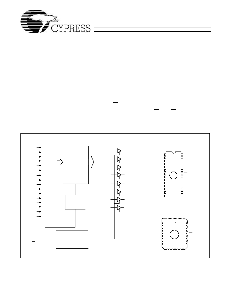
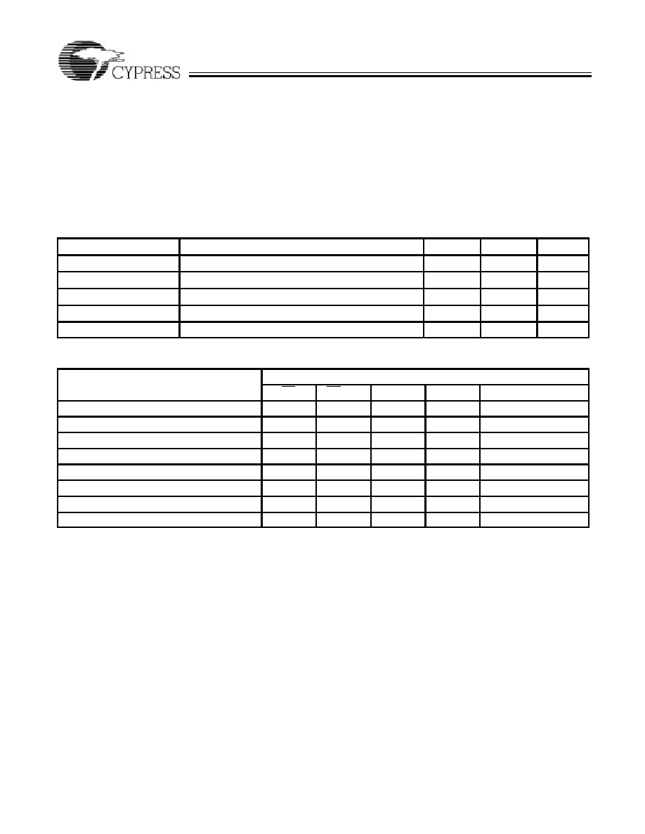
Logic Block Diagram
Pin Configurations
Features
D
CMOS for optimum speed/power
D
High speed
t
AA
= 25 ns max. (commercial)
t
AA
= 35 ns max. (military)
D
Low power
275 mW max.
Less than 85 mW when deselected
D
Byte wide memory organization
D
100% reprogrammable in the
windowed package
D
EPROM technology
D
Capable of withstanding >2001V
static discharge
D
Available in
32 pin PLCC
28 pin TSOP I
28 pin, 600 mil plastic or
hermetic DIP
32 pin hermetic LCC
Functional Description
The CY27H512 is a high performance,
512K CMOS EPROM organized in 64
Kbytes. It is available in industry standard
28 pin, 600 mil DIP, 32 pin LCC and
PLCC, and 28 pin TSOP I packages.
These devices offer high density storage
combined with 40 MHz performance. The
CY27H512 is available in windowed and
opaque packages. Windowed packages al
low the device to be erased with UV light
for 100% reprogrammability.
The CY27H512 is equipped with a power
down chip enable (CE) input and output
enable (OE). When CE is deasserted, the
device powers down to a low power stand
by mode. The OE pin three states the out
puts without putting the device into stand
by mode. While CE offers lower power,
OE provides a more rapid transition to and
from three stated outputs.
The memory cells utilize proven EPROM
floating gate technology and byte wide in
telligent programming algorithms. The
EPROM cell requires only 12.75 V for the
supervoltage and low programming cur
rent allows for gang programming. The de
vice allows for each memory location to be
tested 100%, because each location is writ
ten to, erased, and repeatedly exercised
prior to encapsulation. Each device is also
tested for AC performance to guarantee
that the product will meet DC and AC
specification limits after customer pro
gramming.
The CY27H512 is read by asserting both
the CE and the OE inputs. The contents of
the memory location selected by the ad
dress on inputs A
15
-A
0
will appear at the
outputs O
7
-O
0
.
Top View
DIP
H512 1
H512 2
Top View
H512 3
PROGRAMMABLE
ARRAY
O
0
O
1
O
7
O
2
O
4
O
3
O
5
O
6
ADDRESS
DECODER
A
0
A
1
A
2
A
3
A
4
A
5
A
6
A
8
A
7
MULTIPLEXER
A
9
A
10
A
11
A
12
A
13
A
14
A
15
OUTPUT ENABLE
DECODER
CE
OE
POWER DOWN
1
2
3
4
5
6
7
8
9
10
11
12
16
17
18
19
20
24
23
22
21
13
14
25
28
27
26
A
15
A
12
A
7
A
6
A
5
A
4
A
3
A
2
A
1
A
0
O
0
O
1
O
2
GND
V
CC
A
14
A
13
A
8
A
9
A
11
OE/V
PP
A
10
CE
O
7
O
6
O
4
O
5
O
3
15
12
O
0
31
4
5
6
7
8
9
10
3 2 1
30
13
14 15 16 17
26
25
24
23
22
21
11
A
7
V CC
A
6
A
5
A
4
A
3
A
2
A
1
A
0
CE
A
9
A
11
NC
A
10
O
7
O
6
O
5
GND
A
8
OE/V
PP
A
12
O 4
O 2
O 1
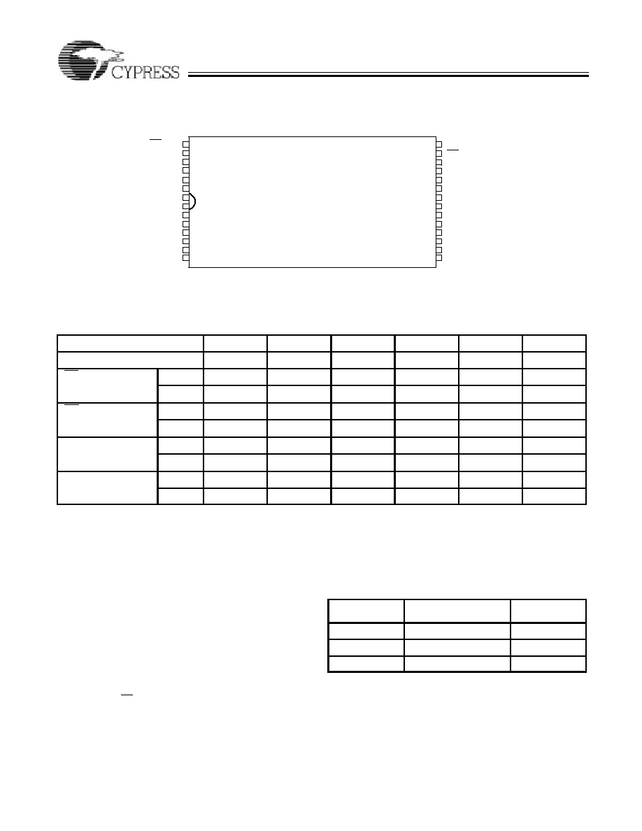
1819 20
27
28
29
32
NC
O 3
A
15
A
14
A
13
DU
DU
LCC/PLCC
[1]
CY27H512
PRELIMINARY
2
22
23
24
25
26
27
28
1
2
3
4
7
8
9
13
12
11
10
14
17
16
15
Top View
TSOP
5
6
18
21
20
19
A
11
A
9
A
8
A
13
A
14
V
CC
A
15
A
12
A
7
A
6
A
5
A
4
A
3
A
10
CE
O
7
O
6
O
5
O
4
O
3
GND
O
2
O
1
A
0
O
0
A
1
OE/V
PP
Pin Configurations
(continued)
H512 4
A
2
Type 1
Selection Guide
27H512-25
27H512-30
27H512-35
27H512-45
27H512-55
27H512-70
Maximum Access Time (ns)
25
30
35
45
55
70
CE Access Time (ns)
Com'l
30
35
35
45
55
70
Mil
40
45
55
70
OE Access Time (ns)
Com'l
12
15
15
15
20
25
Mil
20
20
20
25
I
CC[2]
(mA)
Power Supply Current
Com'l
75
75
50
50
50
50
Power Supply Current
Mil
85
60
60
60
I
SB[3]
(mA)
Stand by Current
Com'l
15
15
15
15
15
15
Stand by Current
Mil
25
25
25
25
Maximum Ratings
(Above which the useful life may be impaired. For user guidelines,
not tested.)
Storage Temperature
-65_C to +150_C
. . . . . . . . . . . . . . . . . . .
Ambient Temperature with
Power Applied
-55_C to +125_C
. . . . . . . . . . . . . . . . . . . . . . . .
Supply Voltage to Ground Potential
-0.5V to +7.0V
. . . . . . . . .
DC Voltage Applied to Outputs
in High Z State
-0.5V to +5.5V
. . . . . . . . . . . . . . . . . . . . . . . . . .
DC Input Voltage
-3.0V to +7.0V
. . . . . . . . . . . . . . . . . . . . . . . .
Transient Input Voltage
-3.0V for <20 ns
. . . . . . . . . . . . . . . . .
DC Program Voltage
13.0V
. . . . . . . . . . . . . . . . . . . . . . . . . . . . . .
UV Erasure
7258 Wsec/cm
2
. . . . . . . . . . . . . . . . . . . . . . . . . . . . . .
Static Discharge Voltage
>2001V
. . . . . . . . . . . . . . . . . . . . . . . .
(per MIL STD 883, Method 3015)
Latch Up Current
>200 mA
. . . . . . . . . . . . . . . . . . . . . . . . . . . .
Operating Range
Range
Ambient
Temperature
V
CC
Commercial
0_C to +70_C
5V � 10%
Industrial
[4]
-40_C to +85_C
5V � 10%
Military
[5]
-55_C to +125_C
5V � 10%
Notes:
2. V
CC
= Max., I
OUT
= 0 mA, f=10 MHz.
3. V
CC
= Max., CE = V
IH
.
4. Contact a Cypress representative for industrial temperature range
specification.
5. T
A
is the instant on" case temperature.
CY27H512
PRELIMINARY
3
Electrical Characteristics
Over the Operating Range
[6, 7]
27H512-25
27H512-30
27H512-35
27H512-45
27H512-55
27H512-70
Parameter
Description
Test Conditions
Min.
Max.
Min.
Max.
Min.
Max.
Unit
V
OH
Output HIGH
Voltage
V
CC
= Min., I
OH
= -4.0 mA
2.4
2.4
2.4
V
V
OL
Output LOW Voltage
V
CC
= Min., I
OL
= 12.0 mA
0.45
0.45
0.45
V
V
IH
Input HIGH Level
Guaranteed Input Logical
HIGH Voltage for All Inputs
2.0
V
CC
+0.5 2.0
V
CC
+0.5 2.0
V
CC
+0.5
V
V
IL
Input LOW Level
Guaranteed Input Logical
LOW Voltage for All Inputs
0.8
0.8
0.8
V
I
IX
Input Leakage
Current
GND < V
IN
< V
CC
-10
+10
-10
+10
-10
+10
mA
I
OZ
Output Leakage
Current
GND < V
OUT
< V
CC
,
Output Disable
-10
+10
-10
+10
-10
+10
mA
I
CC
Power Supply Current
V
CC
=Max.,
I
OUT
=0 mA,
Com'l
75
50
50
mA
I
OUT
=0 mA,
f=10 MHz
Mil
85
60
mA
I
SB
Stand By Current
V
CC
=Max.,
CE = V
IH
Com'l
15
15
15
mA
CE = V
IH
Mil
25
25
mA
Capacitance
[7]
Parameter
Description
Test Conditions
Max.
Unit
C
IN
Input Capacitance
T
A
= 25_C, f = 1 MHz,
V
CC
= 5.0V
10
pF
C
OUT
Output Capacitance
V
CC
= 5.0V
10
pF
Notes:
6. See the last page of this specification for Group A subgroup testing in
formation.
7. See Introduction to CMOS PROMs in this Data Book for general in
formation on testing.
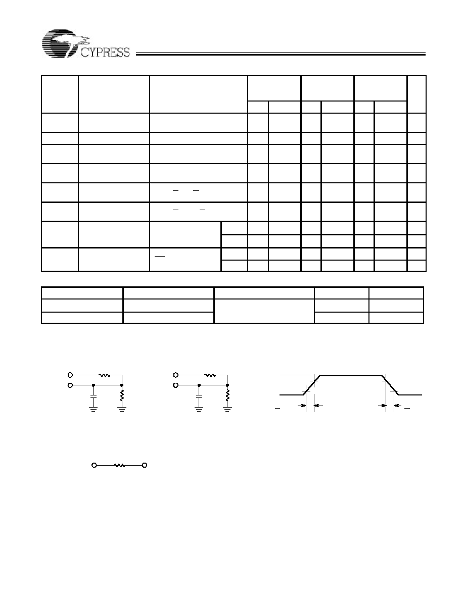
AC Test Loads and Waveforms
H512 5
H512 6
90%
10%
3.0V
GND
90%
10%
ALL INPUT PULSES
5V
OUTPUT
30 pF
INCLUDING
JIG AND
SCOPE
5V
OUTPUT
5 pF
INCLUDING
JIG AND
SCOPE
(a)
(b)
< 3 ns
< 3 ns
OUTPUT
R1 318W
R2
197W
121W
Equivalent to:
TH�VENIN EQUIVALENT
1.91V
R1 318W
R2
197W
CY27H512
PRELIMINARY
4
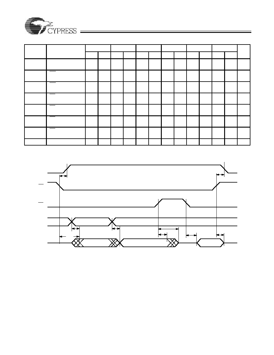
Switching Characteristics
Over the Operating Range
27H512-25 27H512-30 27H512-35 27H512-45 27H512-55 27H512-70
Parameter
Description
Min. Max. Min. Max. Min. Max. Min. Max. Min. Max. Min. Max. Unit
t
AA
Address to Output
Valid
25
30
35
45
55
70
ns
t
OE
OE Active to
Output Valid
12
15
15
15
20
25
ns
t
HZOE
OE Inactive to
High Z
12
15
15
15
20
25
ns
t
CE
CE Active to
Output Valid
30
35
35
45
55
70
ns
t
HZCE
CE Inactive to
High Z
12
15
15
15
20
25
ns
t
PU
CE Active to
Power Up
0
0
0
0
0
0
ns
t
PD
CE Inactive to
Power Down
30
35
40
40
50
60
ns
t
OH
Output Data Hold
0
0
0
0
0
0
ns
Switching Waveform
H512 7
t
PU
t
CE
t
AA
t
PD
CE
O
0
-O
7
A
0
- A
15
OE
I
CC
ADDR A
ADDR B
t
AA
DATA A
DATA B
DATA B
t
HZOE
t
OE
t
HZCE
t
OH
CY27H512
PRELIMINARY
5
Erasure Characteristics
Wavelengths of light less than 4000 Angstroms begin to erase the
CY27H512 in the windowed package. For this reason, an opaque
label should be placed over the window if the EPROM is exposed
to sunlight or fluorescent lighting for extended periods of time.
The recommended dose of ultraviolet light for erasure is a wave
length of 2537 Angstroms for a minimum dose (UV intensity mul
tiplied by exposure time) of 25 Wsec/cm
2
. For an ultraviolet lamp
with a 12 mW/cm
2
power rating, the exposure time would be ap
proximately 35 minutes. The CY27H512 needs to be within 1 inch
of the lamp during erasure. Permanent damage may result if the
EPROM is exposed to high intensity UV light for an extended pe
riod of time. 7258 Wsec/cm
2
is the recommended maximum
dosage.
Programming Modes
Programming support is available from Cypress as well as from a
number of third party software vendors. For detailed program
ming information, including a listing of software packages, please
see the PROM Programming Information located at the end of
this section. Programming algorithms can be obtained from any
Cypress representative.
Table 1. Programming Electrical Characteristics
Parameter
Description
Min.
Max.
Unit
V
PP
Programming Power Supply
12.5
13
V
I
PP
Programming Supply Current
50
mA
V
IHP
Programming Input Voltage HIGH
3.0
V
CC
V
V
ILP
Programming Input Voltage LOW
-0.5
0.4
V
V
CCP
Programming VCC
6.0
6.5
V
Table 2. Mode Selection
Pin Function
[8]
Mode
CE
OE/V
PP
A
0
A
9
Data
Read
V
IL
V
IL
A
0
A
9
O
7
- O
0
Output Disable
X
V
IH
A
0
A
9
High Z
Stand by
V
IH
X
X
X
High Z
Program
V
ILP
V
PP
A
0
A
9
D
7
- D
0
Program Verify
V
ILP
V
ILP
A
0
A
9
O
7
- O
0
Program Inhibit
V
IHP
V
PP
A
0
A
9
High Z
Signature Read (MFG)
V
IL
V
IL
V
IL
V
HV[9]
34H
Signature Read (DEV)
V
IL
V
IL
V
IH
V
HV[9]
1FH
Note:
8. X can be V
IL
or V
IH
.
9. V
HV
=12�0.5V
CY27H512
PRELIMINARY
6
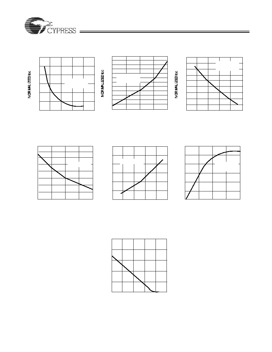
Typical DC and AC Characteristics
CLOCK PERIOD (ns)
NORMALIZED SUPPLY CURRENT
vs. CYCLE PERIOD
NORMALIZED ACCESS TIME
vs. AMBIENT TEMPERATURE
NORMALIZED SUPPLY CURRENT
vs. SUPPLY VOLTAGE
SUPPLY VOLTAGE (V)
AMBIENT TEMPERATURE (_C)
OUTPUT SOURCE CURRENT
vs. OUTPUT VOLTAGE
NORMALIZED ACCESS
TIME
NORMALIZED ACCESS TIME
vs. SUPPLY VOLTAGE
120
100
60
40
20
0.0
1.0
2.0
3.0
4.0
OUTPUT SINK CURRENT (mA)
0
80
OUTPUT SINK CURRENT
vs. OUTPUT VOLTAGE
V
CC
= 5.0V
T
A
= 25_C
-100
-80
-60
-40
-20
0.0
1.0
2.0
3.0
4.0
OUTPUT SOURCE CURRENT
OUTPUT VOLTAGE (V)
OUTPUT SOURCE CURRENT vs.
OUTPUT VOLTAGE
0.0
5.0
SUPPLY VOLTAGE (V)
AMBIENT TEMPERATURE (_C)
OUTPUT VOLTAGE (V)
H512 8
1.1
1.0
0.9
0.8
0.7
0.6
0.0
50
100
150
200
0.5
250
1.7
1.3
1.1
0.7
0.6
4
4.5
5
5.5
6
0.5
V
CC
= 5.5V
T
A
= 25_C
f = 10 MHz
T
A
= 25_C
0.8
0.9
1.0
1.2
1.4
1.5
1.6
1.25
1.2
1.1
1.0
0.9
0.85
-100 -50
0
50
100
0.8
150
V
CC
= 5.5V
f = 10 MHz
0.95
1.05
1.15
1.15
1.1
1.0
0.95
0.9
4
4.5
5
5.5
6
0.85
1.05
T
A =
25_C
1.2
1.25
1.4
1.3
1.2
1.1
1.0
0.9
-100 -50
0
50
100
0.8
150
V
CC
= 4.5V
NORMALIZED ACCESS
TIME
CY27H512
PRELIMINARY
7
Ordering Information
[10]
Speed
(ns)
Ordering Code
Package
Name
Package Type
Operating
Range
25
CY27H512-25HC
H65
32 Pin Windowed Leaded Chip Carrier
Commercial
CY27H512-25JC
J65
32 Lead Plastic Leaded Chip Carrier
CY27H512-25ZC
Z28
28 Lead Thin Small Outline Package
30
CY27H512-30HC
H65
32 Pin Windowed Leaded Chip Carrier
Commercial
CY27H512-30JC
J65
32 Lead Plastic Leaded Chip Carrier
CY27H512-30PC
P15
28 Lead (600 Mil) Molded DIP
CY27H512-30WC
W16
28 Lead (600 Mil) Windowed CerDIP
CY27H512-30ZC
Z28
28 Lead Thin Small Outline Package
35
CY27H512-35HC
H65
32 Pin Windowed Leaded Chip Carrier
Commercial
CY27H512-35JC
J65
32 Lead Plastic Leaded Chip Carrier
CY27H512-35PC
P15
28 Lead (600 Mil) Molded DIP
CY27H512-35WC
W16
28 Lead (600 Mil) Windowed CerDIP
CY27H512-35ZC
Z28
28 Lead Thin Small Outline Package
CY27H512-35HMB
H65
32 Pin Windowed Leaded Chip Carrier
Military
CY27H512-35LMB
L55
32 Pin Rectangular Leadless Chip Carrier
CY27H512-35QMB
Q55
32 Pin Windowed Rectangular Leadless Chip Carrier
45
CY27H512-45HC
H65
32 Pin Windowed Leaded Chip Carrier
Commercial
CY27H512-45JC
J65
32 Lead Plastic Leaded Chip Carrier
CY27H512-45PC
P15
28 Lead (600 Mil) Molded DIP
CY27H512-45WC
W16
28 Lead (600 Mil) Windowed CerDIP
CY27H512-45ZC
Z28
28 Lead Thin Small Outline Package
CY27H512-45DMB
D16
28 Lead (600 Mil) CerDIP
Military
CY27H512-45HMB
H65
32 Pin Windowed Leaded Chip Carrier
CY27H512-45LMB
L55
32 Pin Rectangular Leadless Chip Carrier
CY27H512-45QMB
Q55
32 Pin Windowed Rectangular Leadless Chip Carrier
CY27H512-45WMB
W16
28 Lead (600 Mil) Windowed CerDIP
55
CY27H512-55HC
H65
32 Pin Windowed Leaded Chip Carrier
Commercial
CY27H512-55JC
J65
32 Lead Plastic Leaded Chip Carrier
CY27H512-55PC
P15
28 Lead (600 Mil) Molded DIP
CY27H512-55WC
W16
28 Lead (600 Mil) Windowed CerDIP
CY27H512-55ZC
Z28
28 Lead Thin Small Outline Package
CY27H512-55DMB
D16
28 Lead (600 Mil) CerDIP
Military
CY27H512-55HMB
H65
32 Pin Windowed Leaded Chip Carrier
CY27H512-55LMB
L55
32 Pin Rectangular Leadless Chip Carrier
CY27H512-55QMB
Q55
32 Pin Windowed Rectangular Leadless Chip Carrier
CY27H512-55WMB
W16
28 Lead (600 Mil) Windowed CerDIP
Notes:
10. Most of the above products are available in industrial temperature
range. Contact a Cypress representative for specifications and prod
uct availability.
CY27H512
PRELIMINARY
8
Ordering Information
[10]
(continued)
Speed
(ns)
Ordering Code
Package
Name
Package Type
Operating
Range
70
CY27H512-70HC
H65
32 Pin Windowed Leaded Chip Carrier
Commercial
CY27H512-70JC
J65
32 Lead Plastic Leaded Chip Carrier
CY27H512-70PC
P15
28 Lead (600 Mil) Molded DIP
CY27H512-70WC
W16
28 Lead (600 Mil) Windowed CerDIP
CY27H512-70ZC
Z28
28 Lead Thin Small Outline Package
CY27H512-70DMB
D16
28 Lead (600 Mil) CerDIP
Military
CY27H512-70HMB
H65
32 Pin Windowed Leaded Chip Carrier
CY27H512-70LMB
L55
32 Pin Rectangular Leadless Chip Carrier
CY27H512-70QMB
Q55
32 Pin Windowed Rectangular Leadless Chip Carrier
CY27H512-70WMB
W16
28 Lead (600 Mil) Windowed CerDIP
MILITARY SPECIFICATIONS
Group A Subgroup Testing
DC Characteristics
Parameter
Subgroups
V
OH
1, 2, 3
V
OL
1, 2, 3
V
IH
1, 2, 3
V
IL
1, 2, 3
I
IX
1, 2, 3
I
OZ
1, 2, 3
I
CC
1, 2, 3
I
SB
1, 2, 3
Switching Characteristics
Parameter
Subgroups
t
AA
7, 8, 9, 10, 11
t
OE
7, 8, 9, 10, 11
t
CE
7, 8, 9, 10, 11
Document #: 38-00422

CY27H512
PRELIMINARY
9
Package Diagrams
(continued)
28 Lead (600 Mil) CerDIP D16
MIL-STD-1835 D-10 Config. A
32 Pin Rectangular Leadless Chip Carrier L55
MIL-STD-1835 C-12
32 Lead Plastic Leaded Chip Carrier J65
32 Pin Windowed Rectangular Leadless Chip Carrier Q55
MIL-STD-1835 C-12

CY27H512
PRELIMINARY
10
Package Diagrams
32 Pin Windowed Leaded Chip Carrier H65
28 Lead (600 Mil) Molded DIP P15
CY27H512
PRELIMINARY
11
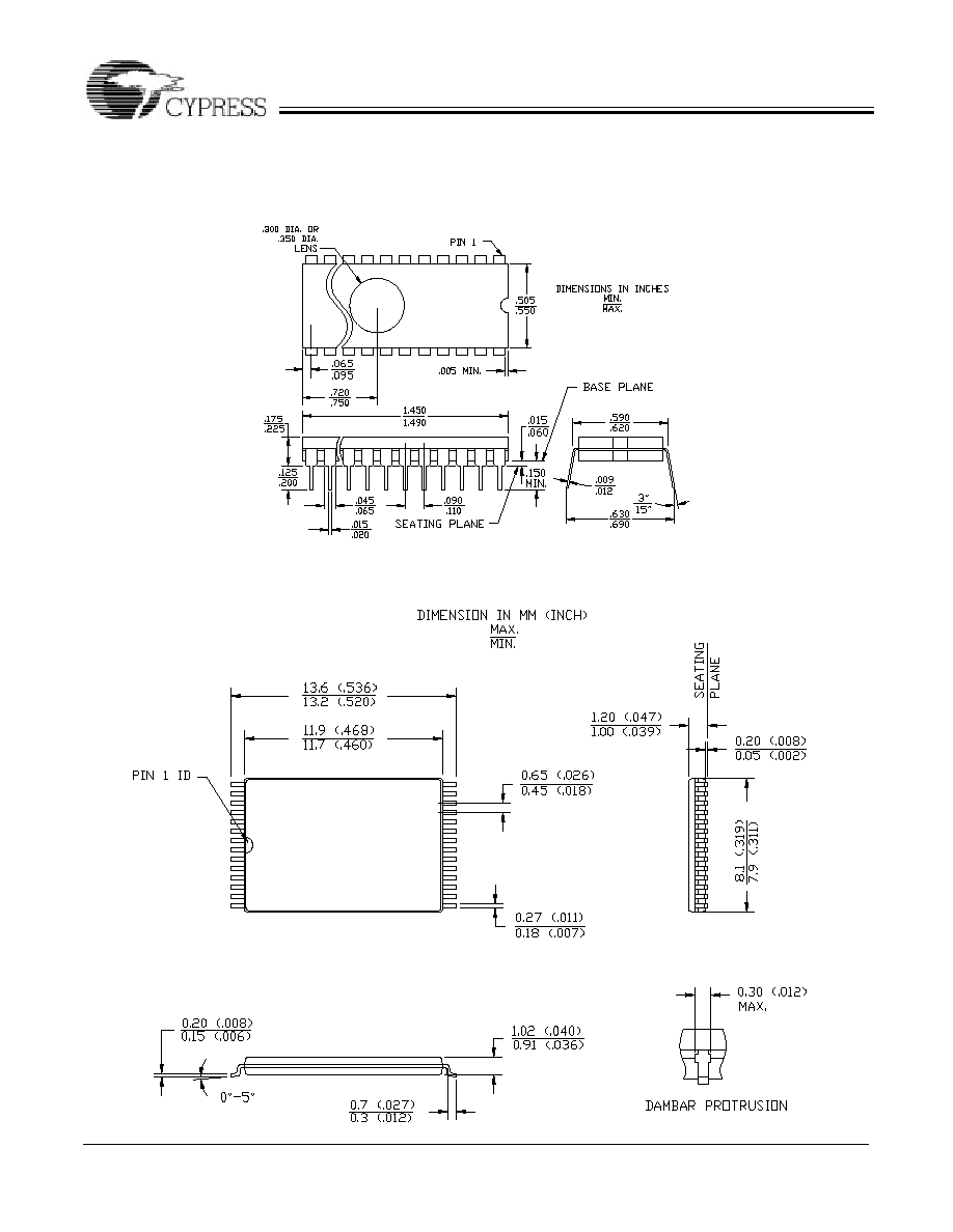
Package Diagrams
28 Lead (600 Mil) Windowed CerDIP W16
MIL-STD-1835 D-10 Config. A
28 Lead Thin Small Outline Package Z28
E
Cypress Semiconductor Corporation, 1994. The information contained herein is subject to change without notice. Cypress Semiconductor Corporation assumes no responsibility for
the use of any circuitry other than circuitry embodied in a Cypress Semiconductor Corporation product. Nor does it convey or imply any license under patent or other rights. Cypress Semicon
ductor does not authorize its products for use as critical components in life support systems where a malfunction or failure of the product may reasonably be expected to result in significant
injury to the user. The inclusion of Cypress Semiconductor products in life support systems applications implies that the manufacturer assumes all risk of such use and in so doing indemnifies
Cypress Semiconductor against all damages.