Spread Spectrum Timing Solution for Serverworks Chipset
CY28158
Cypress Semiconductor Corporation
∑
3901 North First Street
∑
San Jose
∑
CA 95134
∑
408-943-2600
Document #: 38-07039 Rev. *B
Revised June 25, 2004
Features
∑ Maximized EMI suppression using Cypress's spread
spectrum technology
∑ Based on Industry Standard CK133 Pinout with all out-
puts compliant to CK98 specifications
∑ 0.5% downspread outputs deliver up to 10dB lower EMI
∑ 6 skew-controlled copies of CPU output
∑ 6 copies of PCI output (synchronous w/CPU output)
∑ 2 copies of 66 MHz fixed frequency 3.3V clock
∑ 3 copies of 16.67 MHz IOAPIC clock, synchronous to
CPU clock
∑ 1 copy of 48 MHz USB output
∑ 2 copies of 14.31818 MHz reference clock
∑ Programmable to 133 or 100 MHz operation
∑ Power management control pins for clock stop and
shut down
∑ Available in 56-pin SSOP
Key Specifications
Supply Voltages:...................................... V
DD33
= 3.3V ± 5%
................................................................ V
DD25
= 2.5V ± 5%
CPU Output Jitter: ....................................................<150 ps
CPU Output Skew: ....................................................<175 ps
CPU to 3V66 Output Offset: 0.0 to1.5 ns (CPU leads)
CPU to IOAPIC Output Offset 1.5 to 4.0 ns (CPU leads)
CPU to PCI Output Offset................. 0 to 4.0 ns (CPU leads)
Table 1. Pin Selectable Frequency.
SEL133/100#
CPU0:5 (MHz)
PCI
1
133
33.3
0
100
33.3
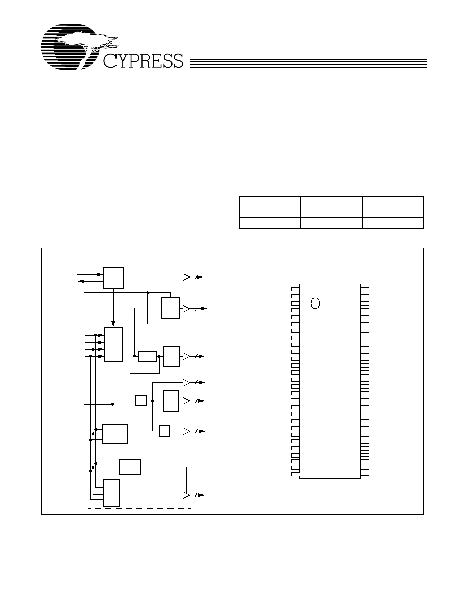
Block Diagram
Pin Configuration
GND_REF
REF0
REF1
VDD_REF
X1
X2
GND_PCI
GND_PCI
PCI_F
VDD_PCI
PCI1
PCI2
GND_PCI
PCI3
PCI4
VDD_PCI
VDD_PCI
PCI5
GND_PCI
GND_3V66
GND_3V66
VDD_3V66
VDD_3V66
GND_3V66
CY28158
VDD_IOAPIC
IOAPIC2
IOAPIC1
IOAPIC0
GND_IOAPIC
VDD_CPU
CPU5
CPU4
GND_CPU
VDD_CPU
CPU3
CPU2
GND_CPU
VDD_CPU
CPU1
CPU0
GND_CPU
VDDA
GNDA
PCI_STOP#
CPU_STOP#
PWR_DWN#
SPREAD#
SEL1
56
55
54
53
52
51
50
49
48
47
46
45
44
43
42
41
40
39
38
37
36
35
34
33
1
2
3
4
5
6
7
8
9
10
11
12
13
14
15
16
17
18
19
20
21
22
23
24
25
26
27
28
32
31
30
29
3V66_0
3V66_1
VDD_3V66
SEL133/100#
SEL0
VDD_48MHZ
48MHZ
GND_48MHZ
REF0:1
CPU0:5
3V66_0:1
XTAL
PLL 1
SPREAD#
X2
X1
PCI_F
PCI1:5
IOAPIC0:2
PLL2
OSC
STOP
Logic
Power
Tristate
Logic
SEL0
SEL1
SEL133/100#
Clock
CPU_STOP#
˜2/˜1.5
STOP
Logic
Clock
Down
Logic
˜2
STOP
Logic
Clock
˜2
2
6
2
1
5
3
1
PCI_STOP#
PWRDWN#
48MHz

CY28158
Document #: 38-07039 Rev. *B
Page 2 of 10
Pin Definitions
Name
Pins Description
X1
[1]
5
Reference crystal input
X2
[1]
6
Reference crystal feedback
CPU [0≠5]
41, 42, 45, 46, 49, 50
CPU clock outputs
PCI [1≠5]
11, 12, 14, 15, 18
PCI clock outputs, synchronously running at 33.33 MHz
PCI_F
9
Free running PCI clock
3V66 [0≠1]
25, 26
3V66 clock outputs, running at 66.66 MHz
IOAPIC [0≠2]
53, 54, 55
IOAPIC clock outputs, running at 16.67 MHz
REF [0≠1]
2, 3
Reference clock outputs, 14.318 MHz
48MHZ
30
48-MHz USB clock output
CPU_STOP#
36
Active LOW input, disables CPU and 3V66 clocks when asserted
PCI_STOP#
37
Active LOW input, disables PCI clocks when asserted
PWR_DWN#
35
Active LOW input, powers down part when asserted
SPREAD#
34
Active LOW input, enables spread spectrum when asserted
SEL1
33
CPU frequency select input (See Function Table)
SEL0
32
CPU frequency select input (See Function Table)
SEL133/100#
28
CPU frequency select input (See Function Table)
GND_REF
1
3.3V Reference ground
GND_PCI
7, 8, 13, 19
3.3V PCI ground
GND_3V66
20, 21, 24
3.3V 66-MHz (AGP) ground
GND_48MHZ
29
3.3V 48-MHz (USB) ground
GND_IOAPIC
52
2.5V APIC ground
GND_CPU
40, 44, 48
2.5V CPU ground
GNDA
38
Analog ground to PLL and Core
VDD_REF
4
3.3V Reference voltage supply
VDD_PCI
10, 16, 17
3.3V PCI voltage supply
VDD_3V66
22, 23, 27
3.3V 66-MHz (AGP) voltage supply
VDD_48MHZ
31
3.3V 48-MHz (USB) voltage supply
VDD_IOAPIC
56
2.5V APIC voltage supply
VDD_CPU
43, 47, 51
2.5V CPU voltage supply
VDDA
39
Analog voltage supply to PLL and Core
Note:
1.
For best accuracy, use a parallel-resonant crystal, C
LOAD
= 18 pF. For crystals with different C
LOAD
, please refer to the application note, "Crystal Oscillator
Topics."

CY28158
Document #: 38-07039 Rev. *B
Page 3 of 10
Function Table
[2]
SEL133
/100#
SEL1
SEL0
CPU
(MHz)
3V66
(MHz)
PCI
(MHz)
48MHZ
(MHz)
REF
(MHz)
IOAPIC
(MHz)
0
0
0
Hi-Z
Hi-Z
Hi-Z
Hi-Z
Hi-Z
Hi-Z
0
0
1
100.227
[3]
66.818
[3]
33.409
[3]
48.008
[3]
14.318
[3]
16.705
[3]
0
1
0
100
66.67
33.33
OFF
14.318
16.67
0
1
1
100
66.67
33.33
48.008
[3]
14.318
16.67
1
0
0
TCLK/2
TCLK/4
TCLK/8
TCLK/2
TCLK
TCLK/16
1
0
1
N/A
N/A
N/A
N/A
N/A
N/A
1
1
0
133.33
66.67
33.33
OFF
14.318
16.67
1
1
1
133.33
66.67
33.33
48.008
[3]
14.318
16.67
Actual Clock Frequency Values
Clock Output
Target
Frequency
(MHz)
Actual
Frequency
(MHz)
PPM
CPU
100.0
99.126
≠8740
CPU
133.33
132.769
≠4208
48MHZ
48.0
48.008
167
Clock Enable Configuration
CPU_STOP#
PWR_DWN#
PCI_STOP#
CPU
3V66
PCI
PCI_F
REF
IOAPIC
OSC.
VCOs
X
0
X
LOW
LOW
LOW
LOW
LOW
OFF
OFF
0
1
0
LOW
LOW
LOW
ON
ON
ON
ON
0
1
1
LOW
LOW
ON
ON
ON
ON
ON
1
1
0
ON
ON
LOW
ON
ON
ON
ON
1
1
1
ON
ON
ON
ON
ON
ON
ON
Clock Driver Impedances
Impedance
Buffer Name
V
DD
Range
Buffer Type
Minimum
Typical
Maximum
CPU, IOAPIC
2.375V ≠ 2.625V
Type 1
13.5
29
45
48MHZ, REF
3.135V ≠ 3.465V
Type 3
20
40
60
PCI, 3V66
3.135V ≠ 3.465V
Type 5
12
30
55
Note:
2.
TCLK is a test clock driven in on the X1 input in test mode.
3.
This selection is defined as "N/A" or "Reserved."

CY28158
Document #: 38-07039 Rev. *B
Page 4 of 10
Maximum Ratings
(Above which the useful life may be impaired. For user guide-
lines, not tested.)
Supply Voltage ..................................................≠0.5 to +7.0V
Input Voltage .............................................. ≠0.5V to V
DD
+0.5
Storage Temperature (Non-Condensing) ... ≠65
∞C to +150∞C
Max. Soldering Temperature (10 sec) ...................... +260
∞C
Junction Temperature............................................... +150
∞C
Package Power Dissipation.............................................. 1W
Static Discharge Voltage
(per MIL-STD-883, Method 3015) ............................. >2000V
Operating Conditions
[4]
Over which Electrical Parameters are Guaranteed
Parameter
Description
Min.
Max.
Unit
V
DD_REF
, V
DD_PCI
, V
DDA
,
V
DD_3V66
,
V
DD_48MHZ
3.3V Supply Voltages
3.135
3.465
V
V
DD_CPU
CPU Supply Voltage
2.375
2.625
V
V
DD_IOAPIC
IOAPIC Supply Voltage
2.375
2.625
V
T
A
Operating Temperature, Ambient
0
70
∞C
C
L
Max. Capacitive Load on
CPU, 48MHZ, REF, IOAPIC
PCI, 3V66
20
30
pF
f
(REF)
Reference Frequency, Oscillator Nominal Value
14.318
14.318
MHz
Electrical Characteristics
Over the Operating Range
Parameter
Description
Test Conditions
Min. Max. Unit
V
IH
High-level Input Voltage
Except Crystal Pads. Threshold voltage for crystal pads = V
DD
/2
2.0
V
V
IL
Low-level Input Voltage
Except Crystal Pads
0.8
V
V
OH
High-level Output Voltage CPU, IOAPIC
I
OH
= ≠1 mA
2.0
V
48 MHZ, REF, PCI, 3V66
I
OH
= ≠1 mA
2.4
V
OL
Low-level Output Voltage
CPU, IOAPIC
I
OL
= 1 mA
0.4
V
48 MHZ, REF, PCI, 3V66
I
OL
= 1 mA
0.4
I
IH
Input High Current
0 < V
IN
< V
DD
10
µA
I
IL
Input Low Current
0 < V
IN
< V
DD
10
µA
I
OH
High-level Output Current CPU
V
OH
= 2.0V
≠16
mA
≠60
IOAPIC
V
OH
= 2.0V
≠20
≠72
48 MHZ, REF
V
OH
= 2.4V
≠15
≠51
3V66, PCI
V
OH
= 2.4V
≠30
≠100
I
OL
Low-level Output Current
CPU
V
OL
= 0.4V
19
mA
49
IOAPIC
V
OL
= 0.4V
25
58
48 MHZ, REF
V
OL
= 0.4V
10
24
3V66, PCI
V
OL
= 0.4V
20
49
I
OZ
Output Leakage Current
Three-state
10
µA
I
DD2
2.5V Power Supply Cur-
rent
V
DDA
/V
DD33
= 3.465V, V
DD25
= 2.625V, F
CPU
= 133 MHz
90
mA
CY28158
Document #: 38-07039 Rev. *B
Page 5 of 10
I
DD3
3.3V Power Supply Cur-
rent
V
DDA
/V
DD33
= 3.465V, V
DD25
= 2.625V, F
CPU
= 133 MHz
160
mA
I
DDPD2
2.5V Shutdown Current
V
DDA
/V
DD33
= 3.465V, V
DD25
= 2.625V
100
µA
I
DDPD3
3.3V Shutdown Current
V
DDA
/V
DD33
= 3.465V, V
DD25
= 2.625V
200
µA
Switching Characteristics
[5]
Over the Operating Range
Parameter
Output
Description
Test Conditions
Min.
Max.
Unit
t
1
All
Output Duty Cycle
[6]
t
1A
/t
1B
45
55
%
t
2
CPU,
IOAPIC
Rising Edge Rate
Between 0.4V and 2.0V
1.0
4.0
V/ns
t
2
48MHZ, REF
Rising Edge Rate
Between 0.4V and 2.4V
0.5
2.0
V/ns
t
2
PCI, 3V66
Rising Edge Rate
Between 0.4V and 2.4V
1.0
4.0
V/ns
t
3
CPU,
IOAPIC
Falling Edge Rate
Between 2.0V and 0.4V
1.0
4.0
V/ns
t
3
48MHZ, REF
Falling Edge Rate
Between 2.4V and 0.4V
0.5
2.0
V/ns
t
3
PCI, 3V66
Falling Edge Rate
Between 2.4V and 0.4V
1.0
4.0
V/ns
t
6
CPU
CPU-CPU Skew
Measured at 1.25V
175
ps
t
8
IOAPIC
IOAPIC-IOAPIC Skew
Measured at 1.25V
250
ps
t
9
3V66
3V66-3V66 Skew
Measured at 1.5V
250
ps
t
10
PCI
PCI-PCI Skew
Measured at 1.5V
500
ps
t
11
CPU, 3V66
CPU-3V66 Clock Skew
CPU leads. Measured at 1.25V for
2.5V clocks and 1.5V for 3.3V clocks
0
1.5
ns
t
12
3V66, PCI
3V66-PCI Clock Skew
3V66 leads. Measured at 1.5V
0.5
2.5
ns
t
13
CPU, IOAPIC
CPU-IOAPIC Clock Skew
CPU leads. Measured at 1.25V
1.5
4
ns
CPU
Cycle-Cycle Clock Jitter
With all outputs running
150
ps
IOAPIC
Cycle-Cycle Clock Jitter
500
ps
48MHZ
Cycle-Cycle Clock Jitter
500
ps
3V66
Cycle-Cycle Clock Jitter
500
ps
REF
Cycle-Cycle Clock Jitter
1000
ps
CPU, PCI
Settle Time
CPU and PCI clock stabilization from
power-up
3
ms
Notes:
4.
Multiple Supplies: The voltage on any input or I/O pin cannot exceed the power pin during power-up. Power supply sequencing is NOT required.
5.
All parameters specified with loaded outputs.
6.
Duty cycle is measured at 1.5V when V
DD
= 3.3V. When V
DD
= 2.5V, duty cycle is measured at 1.25V.
Electrical Characteristics
Over the Operating Range (continued)
Parameter
Description
Test Conditions
Min. Max. Unit