Clock Generator for Serverworks Grand Champion Chipset Applications
CY28159
Cypress Semiconductor Corporation
∑
3901 North First Street
∑
San Jose
∑
CA 95134
∑
408-943-2600
Document #: 38-07118 Rev. **
Revised January 14, 2002
59
Features
∑ Eight differential CPU clock outputs
∑ One PCI output
∑ One 14.31818-MHz reference clock
∑ Two 48-MHz clocks
∑ All outputs compliant with Intel
Æ
specifications
∑ External resistor for current reference
∑ Selection logic for differential swing control, test mode,
Hi-Z, power-down and spread spectrum
∑ 48-pin SSOP and TSSOP packages
Intel is a registered trademark of Intel Corporation.
Table 1. Frequency Selection
SEL 100/133
S0
S1
CPU(0:7), CPU#(0:7)
3V33
48M(0,1)
Notes
0
0
0
100 MHz
33.3MHz
48 MHz
Normal Operation
0
0
1
100 MHz
33.3MHz
Disable
Test Mode(recommended)
0
1
0
100 MHz
Disable
Disable
Test Mode (optional)
0
1
1
Hi-Z
Hi-Z
Hi-Z
Hi-Z all outputs
1
0
0
133.3MHz
33.3MHz
48 MHz
Optional
1
0
1
133.3MHz
33.3MHz
Disable
Optional
1
1
0
200MHz
33.3MHz
48 MHz
o7ptional
1
1
1
N/A
N/A
N/A
Reserved
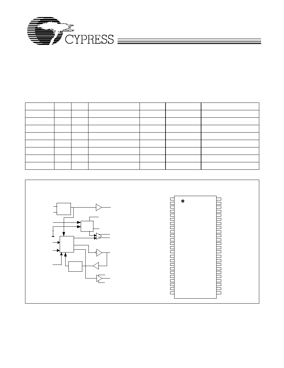
Block Diagram
Pin Configuration
OSC
VCO
I
Control
VDDI
I_Ref
VSSI
REF
CPU (0:7)
CPU (0:7)#
48M(0,1)/S(0,1)
VDDL
3V33
VSSL
SSCG#
SEL100/133
XOUT
XIN
MultSel(0:1)
PD#
S(0,1)
3V33
VDD
48M0/S0
48M1/S1
VSS
VDD
CPU0
CPU0#
VSS
CPU1
CPU1#
VDD
CPU2
CPU2#
VSS
CPU3
CPU3#
VDD
REF
SSCG#
VSS
XIN
XOUT
VDD
SEL100/133
VSS
VDDA
VSSA
PD#
VDD
CPU4
CPU4#
VSS
CPU5
CPU5#
VDD
CPU6
CPU6#
VSS
CPU7
CPU7#
VDD
MULT0
MULT1
VSS
VSSA
IREF
VDDA
1
2
3
4
5
6
7
8
9
10
11
12
13
14
15
16
17
18
19
20
21
22
23
24
48
47
46
45
44
43
42
41
40
39
38
37
36
35
34
33
32
31
30
29
28
27
26
25
CY2
8159
CY28159
Document #: 38-07118 Rev. **
Page 2 of 13
Note:
1.
Definition of I/O column mnemonic on pin description table above 1= Input pin, O = output pin, P = power supply pin, PU = indicates that a bidirectional pin
contains pull-up resistor. This will insure that this pin of the device will be seen by the internal logic as a logic 1 level. Likewise pins with a PD designation are
guaranteed to be seen as a logic 0 level if no external level setting circuitry is present at power up.
Pin Description
Pin
Name
I/O
[1]
Description
20
SSCG
PU
I
When asserted LOW, this pin invokes Spread Spectrum functionality. Spread
spectrum is applicable to CPU(0:7), CPU(0:7)#. This pin has a 250-k
inter-
nal pull-up.
7,10, 13, 16,
42, 39, 36, 33
CPU(0:7)
O
Differential host clock outputs. These outputs are used in pairs, (CPU0-0#,
CPU1-1#, CPU2-2#, CPU3-3#, CPU4-4#, CPU5-5#, CPU6-6#, and CPU7-7#)
for differential clocking of the host bus. CPU(0:7) are 180 degrees out of phase
with their complements, CPU(0:7)#. See Table 1 on page 1
8, 11, 14, 17,
41, 38, 35, 32
CPU(0:7)#
26
IRef
P
This pin establishes the reference current for the internal current steering buff-
ers of the CPU clocks. A resistor is connected from this pin to ground to set
the value of this current.
1
3V33
O
Fixed 33.3-MHz clock output.
44
PD#
PU
I
When asserted LOW, this pin invokes a power-down mode by shutting off all
the clocks, disabling all internal circuitry, and shutting down the crystal oscil-
lator. The 48M(0:1) and REF clocks are driven LOW during this condition and
the CPU clocks are driven HIGH and programmed with an 2X IREF current. It
has a 250-k
internal pull-up.
3, 4
48M(0,1), S(0,1)
IO
S0 and S1 inputs are sensed on power-up and then internally latched. After-
wards the pins are 3V 48-MHz clocks.
48
SEL100/133
PU
I
Input select pin. See Table 1 on page 1.
It has a 250-k
internal Pull-up
23
XOUT
O
Crystal Buffer output pin. Connects to a crystal only. When an external signal
other than a crystal is used or when in Test mode, this pin is kept unconnected.
22
XIN
I
Crystal Buffer input pin. Connects to a crystal, or an external single ended
input clock signal.
19
REF
O
A buffered output clock of the signal applied at Xin. Typically, 14.31818 MHz.
30, 29
Mult(0,1)
I
These input select pins configure the Ioh current (and thus the Voh swing
amplitude) of the CPU clock output pairs. Each pin has a 250-k
internal
Pull-up. See Table 5
for current and resistor values.
25, 46
VDDA
P
3.3V power supply pins.
2, 6, 12, 18,
24, 31, 37, 43
VDD
P
3.3V power supply pins for common supply to the core.
5, 9, 15, 21,
28, 34, 40, 47
VSS
P
Ground pins for common supply to the core.
27, 45
VSSA
P
Ground pins.

CY28159
Document #: 38-07118 Rev. **
Page 3 of 13
Test Load Configuration
The following shows test load configurations for the different Host Clock Outputs.(MULTsel1 = 0, MULTsel0 =1
Table 2. Group Offset Specifications
Group
Offset
Comments
CPU to 3V33
No requirement
CPU to REF
No requirement
Table 3. Group Limits and Parameters (Applicable to all
settings: Sel133/100#=x)
Output Name
Max Load
CPU[(0:7)#]
See Figure 1
REF
20 pF
3V33
30 pF
CPUT
MULTSEL
T
PCB
T
PCB
CPUT#
33
33
Measurement Point
49.9
49.9
2pF
Measurement Point
2pF
221
VDD
Figure 1. 0.7V Test Load Termination
C
LOAD
Probe
Output Under Test
Figure 2. Lumped Load Termination
CY28159
Document #: 38-07118 Rev. **
Page 4 of 13
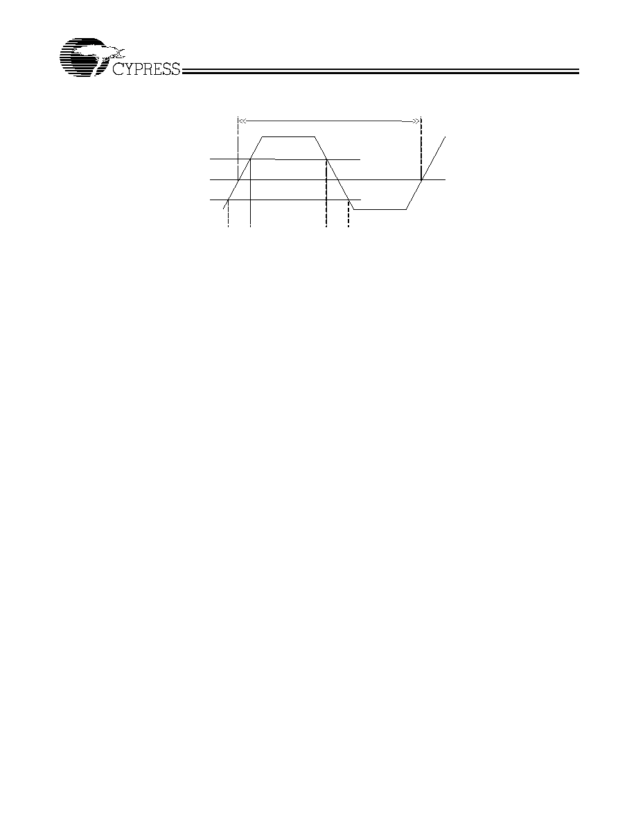
2 . 4 V
0 . 4 V
3 . 3 V
0 V
T r
T f
1 . 5 V
3 . 3 V s i g n a l s
t D C
-
-
Figure 3. 3.3V Measurement Points
CY28159
Document #: 38-07118 Rev. **
Page 5 of 13
Spread Spectrum Clock Generation (SSCG)
Spread Spectrum is a modulation technique applied here for
maximum efficiency in minimizing Electro-Magnetic Interfer-
ence radiation generated from repetitive digital signals mainly
clocks. For a detailed explanation of Spread Spectrum Clock
Generation.
Power Management Functions
Notes:
2.
The entries in boldface are the primary system configurations of interest. The outputs should be optimized for these configurations.
3.
Rr refers to the resistance placed in series with the Iref input and V
SS
.
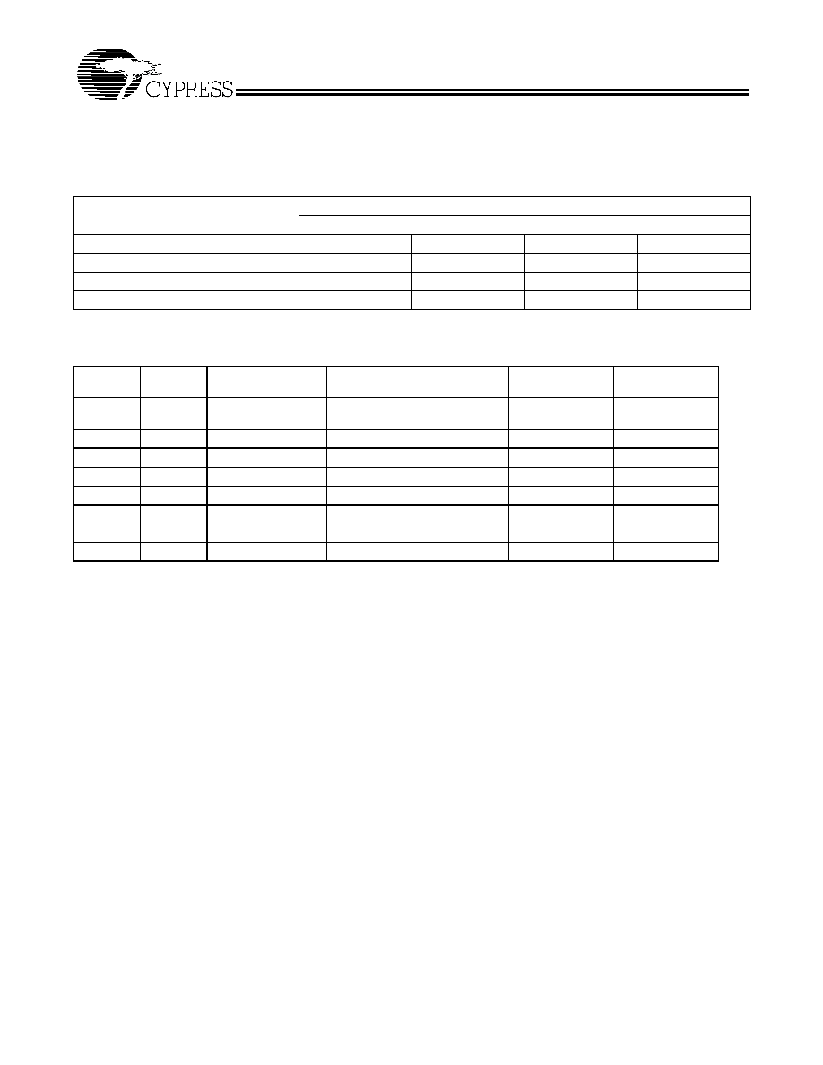
Table 4. Spectrum Spreading Selection Table
Unspread Frequency in MHz
Spread Spectrum Parameter
Downspreading
F Min(MHz)
F Center(MHz)
F Max(MHz)
Spread (%)
100
99.5
99.75
100
≠0.5%
133.3
132.66
132.67
133
≠0.5%
200
199.5
199.75
200
≠0.5%
Table 5. Host Swing Select Functions
[2]
Multsel0
MultSel1
Board Target
Trace/TermZ
Reference Rr, Iref = Vdd(3*Rr)
Note 3
Output Current
Voh@Z, Iref =
2.32 mA
0
0
60 Ohms
Rf = 475 1%,
Iref = 2.32 mA
Ioh = 5*Iref
07V@60
0
0
50 Ohms
Rr = 475 1%,Iref = 2.32 mA
Ioh = 5*Iref
0.59V @ 50
0
1
60 Ohms
Rr = 475 1%,Iref = 2.32 mA
Ioh = 6*Iref
0.85V @ 60
0
1
50 Ohms
Rr = 475 1%,Iref = 2.32 mA
Ioh = 6*Iref
0.71V @ 50
1
0
60 Ohms
Rr = 475 1%,Iref = 2.32 mA
Ioh = 4*Iref
0.56V @ 60
1
0
50 Ohms
Rr = 475 1%,Iref = 2.32 mA
Ioh = 4*Iref
0.47V @ 50
1
1
60 Ohms
Rr = 475 1%,Iref = 2.32 mA
Ioh = 7*Iref
0.99V @ 60
1
1
50 Ohms
Rr = 475 1%,Iref = 2.32 mA
Ioh = 7*Iref
0.82V @ 50