 | –≠–ª–µ–∫—Ç—Ä–æ–Ω–Ω—ã–π –∫–æ–º–ø–æ–Ω–µ–Ω—Ç: CY28316 | –°–∫–∞—á–∞—Ç—å:  PDF PDF  ZIP ZIP |
FTG for VIA PL133T and PLE133T
CY28316
Cypress Semiconductor Corporation
∑
3901 North First Street
∑
San Jose
∑
CA 95134
∑
408-943-2600
Document #: 38-07125 Rev. **
Revised November 9, 2001
16
Features
∑ Single-chip system frequency synthesizer for VIA
PL133T and PLE133T chipsets
∑ Programmable clock output frequency with less than
1 MHz increment
∑ Integrated fail-safe Watchdog Timer for system recov-
ery
∑ Automatically switches to HW-selected or SW-
programmed clock frequency when Watchdog Timer
time-out occurs
∑ Capable of generating system RESET after a Watchdog
Timer time-out occurs or a change in output frequency
via SMBus interface
∑ Support SMBus byte Read/Write and block Read/Write
operations to simplify system BIOS development
∑ Vendor ID and Revision ID support
∑ Programmable drive strength for SDRAM and PCI
output clocks
∑ Programmable output skew for CPU, PCI, and SDRAM
∑ Maximized EMI Suppression using Cypress's Spread
Spectrum technology
∑ Available in 48-pin SSOP
Key Specifications
CPU to CPU Output Skew:.......................................... 175 ps
PCI to PCI Output Skew: ............................................. 500 ps
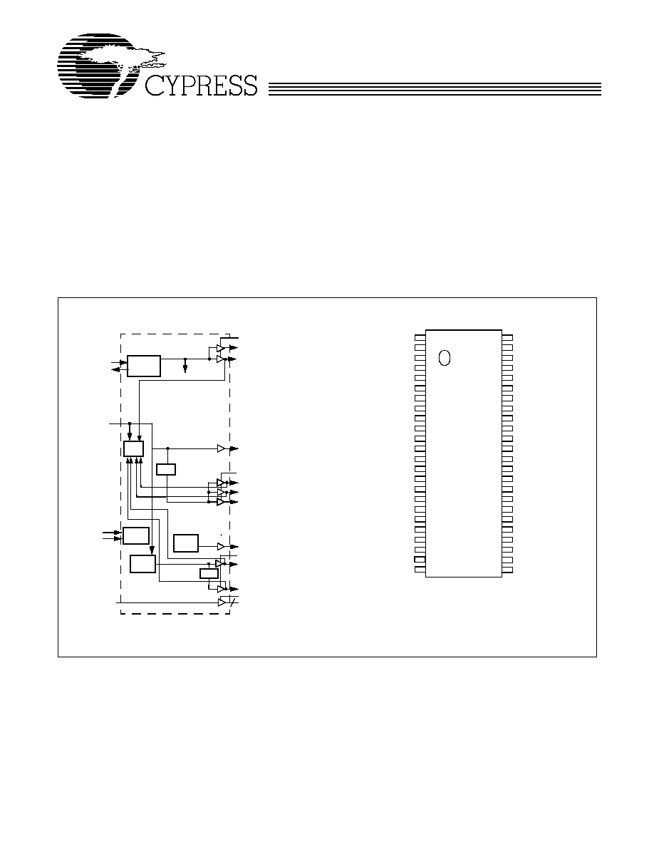
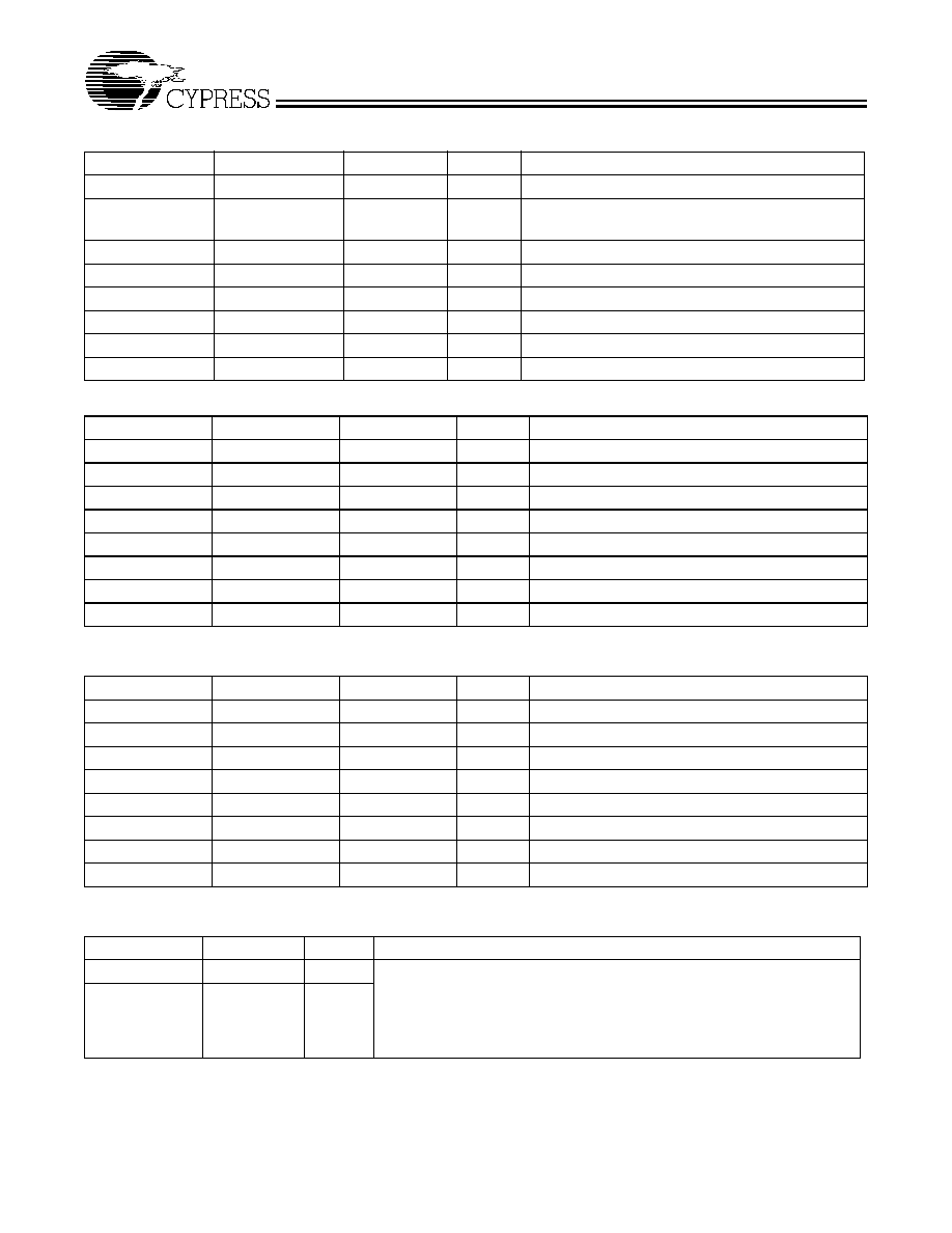
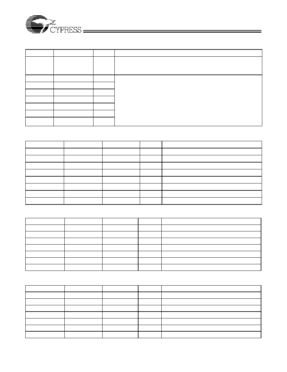
Block Diagram
Pin Configuration
Note:
1.
Signals marked with `*' have internal pull-up resistors.
[1]
VDD_REF
REF0
PCI0/FS4*
XTAL
PLL Ref Freq
PLL 1
X2
X1
REF1/FS2*
VDD_PCI
PCI2:6
48MHz/FS0*
24_48MHz/FS1*
PLL2
˜2,3,4
OSC
VTTPWRGD#
VDD_48MHz
SMBus
SDATA
Logic
SCLK
SDRAM0:12
SDRAMIN
13
VDD_SDRAM
PCI1/FS3*
CPU0:1
˜2
VDD_REF
GND_REF
X1
X2
VDD_PCI
*FS4/PCI0
*FS3/PCI1
GND_PCI
PCI2
PCI3
PCI4
PCI5
PCI6
VDD_PCI
SDRAMIN
GND_SDRAM
SDRAM11
SDRAM10
VDD_SDRAM
SDRAM9
SDRAM8
GND_SDRAM
SDATA
SCLK
C
Y
2831
6
VTT_PWRGD#
REF0
REF1/FS2*
GND_CPU
CPU0
CPU1
VDD_CPU
RST#
SDRAM_12
GND_SDRAM
SDRAM0
SDRAM1
VDD_SDRAM
SDRAM2
SDRAM3
GND_SDRAM
SDRAM4
SDRAM5
VDD_SDRAM
SDRAM6
SDRAM7
VDD_48MHz
48MHz/FS0*
24_48MHz/FS1*
48
47
46
45
44
43
42
41
40
39
38
37
36
35
34
33
32
31
30
29
28
27
26
25
1
2
3
4
5
6
7
8
9
10
11
12
13
14
15
16
17
18
19
20
21
22
23
24
SMBus
{
Logic
Reset
RST#
CY28316
Document #: 38-07125 Rev. **
Page 2 of 20
Pin Definitions
Pin Name
Pin No.
Pin Type
Pin Description
CPU0:1
44, 43
O
CPU Clock Output 0 through 1: CPU clocks for processor and chipset.
PCI2:6
9, 10, 11, 12,
13
O
PCI Clock Outputs 2 through 6: 3.3V 33-MHz PCI clock outputs. Frequency
is set by FS0:4 inputs or through serial data interface.
PCI1/FS3
7
I/O
Fixed PCI Clock Output/Frequency Select 3: 3.3V PCI clock outputs. As an
output, frequency is set by FS0:4 inputs or through the serial data interface. This
pin also serves as a power-on strap option to determine the device operating
frequency, as described in Table 5.
PCI0/FS4
6
I/O
Fixed PCI Clock Output/Frequency Select 4: 3.3V PCI clock outputs. This pin
also serves as a power-on strap option to determine the device operating fre-
quency, as described in Table 5.
RST#
41
O
(open-
drain)
Reset# Output: Open drain system reset output.
48MHz/FS0
26
I/O
48-MHz Output/Frequency Select 0: 3.3V 48-MHz non-spread spectrum out-
put. This pin also serves as a power-on strap option to determine the device
operating frequency as described in Table 5.
24_48MHz/
FS1
25
I/O
24_48MHz Output/Frequency Select 1: 3.3V 24- or 48-MHz non-spread spec-
trum output. This pin also serves as a power-on strap option to determine the
device operating frequency, as described in Table 5.
REF1/FS2
46
I/O
Reference Clock Output 1/Frequency Select 2: 3.3V 14.318-MHz output
clock. This pin also serves as a power-on strap option to determine the device
operating frequency as described in Table 5.
REF0
47
O
Reference Clock Output 0: 3.3V 14.318-MHz output clock.
SDRAMIN
15
I
SDRAM Buffer Input Pin: Reference input for SDRAM buffer.
SDRAM0:12
38, 37, 35,
34, 32, 31,
29, 28, 21,
20, 18, 17, 40
O
SDRAM Outputs: These thirteen dedicated outputs provide copies of the signal
provided at the SDRAMIN input.
SCLK
24
I
Clock pin for SMBus circuitry.
SDATA
23
I/O
Data pin for SMBus circuitry.
X1
3
I
Crystal Connection or External Reference Frequency Input: This pin has
dual functions. It can be used as an external 14.318-MHz crystal connection or
as an external reference frequency input.
X2
4
O
Crystal Connection: An output connection for an external 14.318-MHz crystal.
If using an external reference, this pin must be left unconnected.
VTT_PWRGD#
48
I
VTT_PWRGD#: 3.3V LVTTL compatible input that controls the FS0:4 to be
latched and enables all outputs. CY28316 will sample the FS0:4 inputs and
enable all clock outputs after all V
DD
become valid and VTT_PWRGD# is held
LOW.
VDD_REF,
VDD_PCI,
VDD_SDRAM,
VDD_48MHz
1, 5, 14, 19,
27, 30, 36
P
Power Connection: Power supply for core logic, PLL circuitry, SDRAM outputs,
PCI outputs, reference outputs, 48-MHz output, and 24_48-MHz output. Con-
nect to 3.3V supply.
VDD_CPU
42
P
Power Connection: Power supply for CPU outputs. Connect to 2.5V supply.
GND_REF,
GND_PCI,
GND_SDRAM,
VDD_48MHz,
VDD_CPU
2, 8, 16, 22,
33, 39, 45
G
Ground Connections: Connect all ground pins to the common system ground
plane.
CY28316
Document #: 38-07125 Rev. **
Page 3 of 20
Serial Data Interface
The CY28316 features a two-pin, serial data interface that can
be used to configure internal register settings that control par-
ticular device functions.
Data Protocol
The clock driver serial protocol supports byte/word Write,
byte/word Read, block Write and block Read operations from
the controller. For block Write/Read operation, the bytes must
be accessed in sequential order from lowest to highest byte,
with the ability to stop after any complete byte has been trans-
ferred. For byte/word Write and byte Read operations, the sys-
tem controller can access individual indexed bytes. The offset
of the indexed byte is encoded in the command code.
The definition for the command code is defined in Table 1.
Table 1. Command Code Definition
Bit
Descriptions
7
0 = Block read or block write operation
1 = Byte/Word read or byte/word write operation
6:0
Byte offset for byte/word read or write operation. For block read or write operations, these bits
need to be set at `0000000'.
Table 2. Block Read and Block Write Protocol
Block Write Protocol
Block Read Protocol
Bit
Description
Bit
Description
1
Start
1
Start
2:8
Slave address ≠ 7 bits
2:8
Slave address ≠ 7 bits
9
Write
9
Write
10
Acknowledge from slave
10
Acknowledge from slave
11:18
Command Code ≠ 8 bits
`00000000' stands for block operation
11:18
Command Code ≠ 8 bits
`00000000' stands for block operation
19
Acknowledge from slave
19
Acknowledge from slave
20:27
Byte Count ≠ 8 bits
20
Repeat start
28
Acknowledge from slave
21:27
Slave address ≠ 7 bits
29:36
Data byte 0 ≠ 8 bits
28
Read
37
Acknowledge from slave
29
Acknowledge from slave
38:45
Data byte 1 ≠ 8 bits
30:37
Byte count from slave ≠ 8 bits
46
Acknowledge from slave
38
Acknowledge
...
Data Byte N/Slave Acknowledge...
39:46
Data byte from slave ≠ 8 bits
...
Data Byte N ≠ 8 bits
47
Acknowledge
...
Acknowledge from slave
48:55
Data byte from slave ≠ 8 bits
...
Stop
56
Acknowledge
...
Data bytes from slave/Acknowledge
...
Data byte N from slave ≠ 8 bits
...
Not acknowledge
...
Stop
CY28316
Document #: 38-07125 Rev. **
Page 4 of 20
Table 3. Word Read and Word Write Protocol
Word Write Protocol
Word Read Protocol
Bit
Description
Bit
Description
1
Start
1
Start
2:8
Slave address ≠ 7 bits
2:8
Slave address ≠ 7 bits
9
Write
9
Write
10
Acknowledge from slave
10
Acknowledge from slave
11:18
Command Code - 8 bits
`1xxxxxxx' stands for byte or word operation
bit[6:0] of the command code represents the off-
set of the byte to be accessed
11:18
Command Code ≠ 8 bits
`1xxxxxxx' stands for byte or word operation
bit[6:0] of the command code represents the off-
set of the byte to be accessed
19
Acknowledge from slave
19
Acknowledge from slave
20:27
Data byte low ≠ 8 bits
20
Repeat start
28
Acknowledge from slave
21:27
Slave address ≠ 7 bits
29:36
Data byte high ≠ 8 bits
28
Read
37
Acknowledge from slave
29
Acknowledge from slave
38
Stop
30:37
Data byte low from slave ≠ 8 bits
38
Acknowledge
39:46
Data byte high from slave ≠ 8 bits
47
Not acknowledge
48
Stop
Table 4. Byte Read and Byte Write Protocol
Byte Write Protocol
Byte Read Protocol
Bit
Description
Bit
Description
1
Start
1
Start
2:8
Slave address ≠ 7 bits
2:8
Slave address ≠ 7 bits
9
Write
9
Write
10
Acknowledge from slave
10
Acknowledge from slave
11:18
Command Code - 8 bits
`1xxxxxxx' stands for byte operation
bit[6:0] of the command code represents the off-
set of the byte to be accessed
11:18
Command Code ≠ 8 bits
`1xxxxxxx' stands for byte operation
bit[6:0] of the command code represents the off-
set of the byte to be accessed
19
Acknowledge from slave
19
Acknowledge from slave
20:27
Data byte ≠ 8 bits
20
Repeat start
28
Acknowledge from slave
21:27
Slave address ≠ 7 bits
29
Stop
28
Read
29
Acknowledge from slave
30:37
Data byte from slave ≠ 8 bits
38
Not acknowledge
39
Stop

CY28316
Document #: 38-07125 Rev. **
Page 5 of 20
CY28316 Serial Configuration Map
1. The serial bits will be read by the clock driver in the following
order:
Byte 0 ≠ Bits 7, 6, 5, 4, 3, 2, 1, 0
Byte 1 ≠ Bits 7, 6, 5, 4, 3, 2, 1, 0
Byte N ≠ Bits 7, 6, 5, 4, 3, 2, 1, 0
2. All unused register bits (reserved and N/A) should be writ-
ten to a "0" level.
3. All register bits labeled "Write with 1" must be written to "1"
during initialization.
Byte 0: Control Register 0
Bit
Pin#
Name
Default
Description
Bit 7
≠
Spread Select1
0
See definition in Bit[0]
Bit 6
≠
SEL2
0
See Table 5
Bit 5
≠
SEL1
0
See Table 5
Bit 4
≠
SEL0
0
See Table 5
Bit 3
≠
FS_Override
0
0 = Select operating frequency by FS[4:0] input pins
1 = Select operating frequency by SEL[4:0] settings
Bit 2
≠
SEL4
0
See Table 5
Bit 1
≠
SEL3
0
See Table 5
Bit 0
≠
Spread Select0
0
`00' = OFF
`01' = ≠ 0.5%
`10' = ± 0.5%
`11' = ± 0.25%
Byte 1: Control Register 1
Bit
Pin#
Name
Default
Description
Bit 7
6
Latched FS4 input
X
Latched FS[4:0] inputs. These bits are read-only.
Bit 6
7
Latched FS3 input
X
Bit 5
46
Latched FS2 input
X
Bit 4
25
Latched FS1 input
X
Bit 3
26
Latched FS0 input
X
Bit 2
44
CPU0
1
(Active/Inactive)
Bit 1
43
CPU1
1
(Active/Inactive)
Bit 0
≠
Vendor Test Mode
0
Write with `0'
Byte 2: Control Register 2
Bit
Pin#
Name
Default
Description
Bit 7
40
SDRAM12
1
(Active/Inactive)
Bit 6
6
PCI0
1
(Active/Inactive)
Bit 5
13
PCI6
1
(Active/Inactive)
Bit 4
12
PCI5
1
(Active/Inactive)
Bit 3
11
PCI4
1
(Active/Inactive)
Bit 2
10
PCI3
1
(Active/Inactive)
Bit 1
9
PCI2
1
(Active/Inactive)
Bit 0
7
PCI1
1
(Active/Inactive)
CY28316
Document #: 38-07125 Rev. **
Page 6 of 20
Byte 3: Control Register 3
Bit
Pin#
Name
Default
Description
Bit 7
21, 20, 18, 17
SDRAM8:11
1
(Active/Inactive)
Bit 6
≠
SEL_48MHz
0
0 = 24 MHz
1 = 48 MHz
Bit 5
26
48MHz
1
(Active/Inactive)
Bit 4
25
24_48MHz
1
(Active/Inactive)
Bit 3
29, 28
SDRAM6:7
1
(Active/Inactive)
Bit 2
32, 31
SDRAM4:5
1
(Active/Inactive)
Bit 1
35, 34
SDRAM2:3
1
(Active/Inactive)
Bit 0
38, 37
SDRAM0:1
1
(Active/Inactive)
Byte 4: Control Register 4
Bit
Pin#
Name
Default
Description
Bit 7
≠
Reserved
0
Reserved
Bit 6
≠
Reserved
0
Reserved
Bit 5
≠
Reserved
0
Reserved
Bit 4
≠
Reserved
0
Reserved
Bit 3
≠
Reserved
0
Reserved
Bit 2
≠
Reserved
0
Reserved
Bit 1
≠
Reserved
0
Reserved
Bit 0
≠
Reserved
0
Reserved
Byte 5: Control Register 5
Bit
Pin#
Name
Default
Description
Bit 7
≠
Reserved
0
Reserved
Bit 6
≠
Reserved
0
Reserved
Bit 5
≠
Reserved
0
Reserved
Bit 4
≠
Reserved
0
Reserved
Bit 3
≠
Reserved
0
Reserved
Bit 2
≠
Reserved
0
Reserved
Bit 1
46
REF1
1
(Active/Inactive)
Bit 0
47
REF0
1
(Active/Inactive)
Byte 6: Watchdog Timer Register
Bit
Name
Default
Pin Description
Bit 7
PCI_Skew1
0
PCI skew control
00 = Normal
01 = ≠500 ps
10 = Reserved
11 = +500 ps
Bit 6
PCI_Skew0
0
CY28316
Document #: 38-07125 Rev. **
Page 7 of 20
Bit 5
WD_TIMER4
1
These bits store the time-out value of the Watchdog Timer. The scale of the
timer is determined by the prescaler.
The timer can support a value of 150 ms to 4.8 sec when the prescaler is set
to 150 ms. If the prescaler is set to 2.5 sec, it can support a value from 2.5 sec
to 80 sec.
When the Watchdog Timer reaches "0," it will set the WD_TO_STATUS bit and
generate Reset if RST_EN_WD is enabled.
Bit 4
WD_TIMER3
1
Bit 3
WD_TIMER2
1
Bit 2
WD_TIMER1
1
Bit 1
WD_TIMER0
1
Bit 0
WD_PRE_
SCALER
0
0 = 150 ms
1 = 2.5 sec
Byte 6: Watchdog Timer Register (continued)
Bit
Name
Default
Pin Description
Byte 7: Control Register 7
Bit
Pin#
Name
Default
Pin Description
Bit 7
≠
Reserved
0
Reserved
Bit 6
25
24_48MHz_DRV
1
0 = Norm, 1 = High Drive
Bit 5
26
48MHz_DRV
1
0 = Norm, 1 = High Drive
Bit 4
≠
Reserved
0
Reserved
Bit 3
≠
Reserved
0
Reserved
Bit 2
≠
Reserved
0
Reserved
Bit 1
≠
Reserved
0
Reserved
Bit 0
≠
Reserved
0
Reserved
Byte 8: Vendor ID and Revision ID Register (Read Only)
Bit
Name
Default
Pin Description
Bit 7
Revision_ID3
0
Revision ID bit[3]
Bit 6
Revision_ID2
0
Revision ID bit[2]
Bit 5
Revision_ID1
0
Revision ID bit[1]
Bit 4
Revision_ID0
0
Revision ID bit[0]
Bit 3
Vendor_ID3
1
Bit[3] of Cypress Semiconductor's Vendor ID. This bit is read-only.
Bit 2
Vendor_ID2
0
Bit[2] of Cypress Semiconductor's Vendor ID. This bit is read-only.
Bit 1
Vendor _ID1
0
Bit[1] of Cypress Semiconductor's Vendor ID. This bit is read-only.
Bit 0
Vendor _ID0
0
Bit[0] of Cypress Semiconductor's Vendor ID. This bit is read-only.
Byte 9: System RESET and Watchdog Timer Register
Bit
Name
Default
Pin Description
Bit 7
SDRAM_DRV
0
SDRAM clock output drive strength
0 = Normal
1 = High Drive
Bit 6
PCI_DRV
0
PCI clock output drive strength
0 = Normal
1 = High Drive
Bit 5
Reserved
0
Reserved
CY28316
Document #: 38-07125 Rev. **
Page 8 of 20
Bit 4
RST_EN_WD
0
This bit will enable the generation of a Reset pulse when a Watchdog Timer time-
out occurs.
0 = Disabled
1 = Enabled
Bit 3
RST_EN_FC
0
This bit will enable the generation of a Reset pulse after a frequency change
occurs.
0 = Disabled
1 = Enabled
Bit 2
WD_TO_STATUS
0
Watchdog Timer Time-out Status bit
0 = No time-out occurs (Read); Ignore (Write)
1 = Time-out occurred (Read); Clear WD_TO_STATUS (Write)
Bit 1
WD_EN
0
0 = Stop and reload Watchdog Timer. Unlock CY28316 from recovery frequency
mode.
1 = Enable Watchdog Timer. It will start counting down after a frequency change
occurs.
Note: CY28316 will generate a system Reset, reload a recovery frequency, and
lock itself into a recovery frequency mode after a Watchdog Timer time-out oc-
curs. Under recovery frequency mode, CY28316 will not respond to any attempt
to change output frequency via the SMBus control bytes. System software can
unlock CY28316 from its recovery frequency mode by clearing the WD_EN bit.
Bit 0
CPU0:1_DRV
0
CPU0:1 clock output drive strength
0 = Normal
1 = High Drive
Byte 9: System RESET and Watchdog Timer Register (continued)
Bit
Name
Default
Pin Description
Byte 10: Skew Control Register
Bit
Name
Default
Description
Bit 7
CPU0:1_Skew2
0
CPU0:1 output skew control.
000 = Normal
001 = ≠150 ps
010 = ≠300 ps
011 = ≠450 ps
100 = +150 ps
101 = +300 ps
110 = +450 ps
111 = +600 ps
Bit 6
CPU0:1_Skew1
0
Bit 5
CPU0:1_Skew0
0
Bit 4
Reserved
0
Reserved
Bit 3
Reserved
0
Reserved
Bit 2
Reserved
0
Reserved
Bit 1
Reserved
0
Reserved
Bit 0
Reserved
0
Reserved
CY28316
Document #: 38-07125 Rev. **
Page 9 of 20
Byte 11: Recovery Frequency N-Value Register
Bit
Name
Default
Pin Description
Bit 7
ROCV_FREQ_N7
0
If ROCV_FREQ_SEL is set, CY28316 will use the values programmed in
ROCV_FREQ_N[7:0] and ROCV_FREQ_M[6:0] to determine the recovery
CPU output frequency.when a Watchdog Timer time-out occurs
The setting of FS_Override bit determines the frequency ratio for CPU and
PCI. When it is cleared, CY28316 will use the same frequency ratio stated in
the Latched FS[4:0] register. When it is set, CY28316 will use the frequency
ratio stated in the SEL[4:0] register.
CY28316 supports programmable CPU frequencies ranging from 50 MHz to
248 MHz.
CY28316 will change the output frequency whenever there is an update to
either ROCV_FREQ_N[7:0] or ROCV_FREQ_M[6:0]. Therefore it is
recommended to use word or block Write to update both registers within the
same SMBus bus operation.
Bit 6
ROCV_FREQ_N6
0
Bit 5
ROCV_FREQ_N5
0
Bit 4
ROCV_FREQ_N4
0
Bit 3
ROCV_FREQ_N3
0
Bit 2
ROCV_FREQ_N2
0
Bit 1
ROCV_FREQ_N1
0
Bit 0
ROCV_FREQ_N0
0
Byte 12: Recovery Frequency M-Value Register
Bit
Name
Default
Pin Description
Bit 7
ROCV_FREQ_SEL
0
ROCV_FREQ_SEL determines the source of the recover frequency when a
Watchdog Timer time-out occurs. The clock generator will automatically
switch to the recovery CPU frequency based on the selection on
ROCV_FREQ_SEL.
0 = From latched FS[4:0]
1 = From the settings of ROCV_FREQ_N[7:0] and ROCV_FREQ_M[6:0]
Bit 6
ROCV_FREQ_M6
0
If ROCV_FREQ_SEL is set, CY28316 will use the values programmed in
ROCV_FREQ_N[7:0] and ROCV_FREQ_M[6:0] to determine the recovery
CPU output frequency when a Watchdog Timer time-out occurs.
The setting of the FS_Override bit determines the frequency ratio for CPU,
SDRAM, and PCI. When it is cleared, CY28316 will use the same frequency
ratio stated in the Latched FS[4:0] register. When it is set, CY28316 will use
the frequency ratio stated in the SEL[4:0] register.
CY28316 supports programmable CPU frequencies ranging from 50 MHz to
248 MHz.
CY28316 will change the output frequency whenever there is an update to
either ROCV_FREQ_N[7:0] or ROCV_FREQ_M[6:0]. Therefore, it is recom-
mended to use word or block Write to update both registers within the same
SMBus bus operation.
Bit 5
ROCV_FREQ_M5
0
Bit 4
ROCV_FREQ_M4
0
Bit 3
ROCV_FREQ_M3
0
Bit 2
ROCV_FREQ_M2
0
Bit 1
ROCV_FREQ_M1
0
Bit 0
ROCV_FREQ_M0
0
Byte 13: Programmable Frequency Select N-Value Register
Bit
Name
Default
Pin Description
Bit 7
CPU_FSEL_N7
0
If Prog_Freq_EN is set, CY28316 will use the values programmed in
CPU_FSEL_N[7:0] and CPU_FSEL_M[6:0] to determine the CPU output fre-
quency. The new frequency will start to load whenever CPU_FSELM[6:0] is
updated.
The setting of the FS_Override bit determines the frequency ratio for CPU,
SDRAM, and PCI. When it is cleared, CY28316 will use the same frequency
ratio stated in the Latched FS[4:0] register. When it is set, CY28316 will use
the frequency ratio stated in the SEL[4:0] register.
CY28316 supports programmable CPU frequencies ranging from 50 MHz to
248 MHz.
Bit 6
CPU_FSEL_N6
0
Bit 5
CPU_FSEL_N5
0
Bit 4
CPU_FSEL_N4
0
Bit 3
CPU_FSEL_N3
0
Bit 2
CPU_FSEL_N2
0
Bit 1
CPU_FSEL_N1
0
Bit 0
CPU_FSEL_N0
0
CY28316
Document #: 38-07125 Rev. **
Page 10 of 20
Byte 14: Programmable Frequency Select M-Value Register
Bit
Name
Default
Description
Bit 7
Pro_Freq_EN
0
Programmable output frequencies enabled
0 = Disabled
1 = Enabled
Bit 6
CPU_FSEL_M6
0
If Prog_Freq_EN is set, CY28316 will use the values programmed in
CPU_FSEL_N[7:0] and CPU_FSEL_M[6:0] to determine the CPU output fre-
quency. The new frequency will start to load whenever CPU_FSELM[6:0] is
updated.
The setting of the FS_Override bit determines the frequency ratio for CPU,
SDRAM, and PCI. When it is cleared, CY28316 will use the same frequency
ratio stated in the Latched FS[4:0] register. When it is set, CY28316 will use
the frequency ratio stated in the SEL[4:0] register.
CY28316 supports programmable CPU frequencies ranging from 50 MHz to
248 MHz.
Bit 5
CPU_FSEL_M5
0
Bit 4
CPU_FSEL_M4
0
Bit 3
CPU_FSEL_M3
0
Bit 2
CPU_FSEL_M2
0
Bit 1
CPU_FSEL_M1
0
Bit 0
CPU_FSEL_M0
0
Byte 15: Reserved Register
Bit
Pin#
Name
Default
Description
Bit 7
≠
Reserved
0
Reserved
Bit 6
≠
Reserved
0
Reserved
Bit 5
≠
Reserved
0
Reserved
Bit 4
≠
Reserved
0
Reserved
Bit 3
≠
Reserved
0
Reserved
Bit 2
≠
Vendor test mode
0
Reserved. Write with `0'
Bit 1
≠
Vendor test mode
1
Test mode. Write with `1'
Bit 0
≠
Vendor test mode
1
Test mode. Write with `1'
Byte 16: Reserved Register
Bit
Pin#
Name
Default
Description
Bit 7
≠
Reserved
0
Reserved
Bit 6
≠
Reserved
0
Reserved
Bit 5
≠
Reserved
0
Reserved
Bit 4
≠
Reserved
0
Reserved
Bit 3
≠
Reserved
0
Reserved
Bit 2
≠
Reserved
0
Reserved
Bit 1
≠
Reserved
0
Reserved
Byte 17: Reserved Register
Bit
Pin#
Name
Default
Description
Bit 7
≠
Reserved
0
Reserved
Bit 6
≠
Reserved
0
Reserved
Bit 5
≠
Reserved
0
Reserved
Bit 4
≠
Reserved
0
Reserved
Bit 3
≠
Reserved
0
Reserved
Bit 2
≠
Reserved
0
Reserved
Bit 1
-
Reserved
0
Reserved
CY28316
Document #: 38-07125 Rev. **
Page 11 of 20
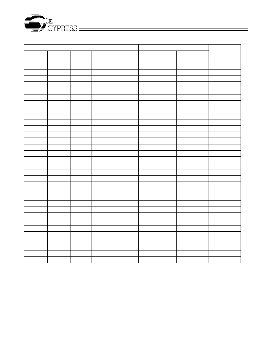
Table 5. Additional Frequency Selections through Serial Data Interface Data Bytes
Input Conditions
Output Frequency
PLL Gear
Constant (G)
FS4
FS3
FS2
FS1
FS0
CPU
PCI
SEL4
SEL3
SEL2
SEL1
SEL0
0
0
0
0
0
200.0
33.3
48.000741
0
0
0
0
1
190.0
38.0
48.000741
0
0
0
1
0
180.0
36.0
48.000741
0
0
0
1
1
170.0
34.0
48.000741
0
0
1
0
0
166.0
33.2
48.000741
0
0
1
0
1
160.0
32.0
48.000741
0
0
1
1
0
150.0
37.5
48.000741
0
0
1
1
1
145.0
36.3
48.000741
0
1
0
0
0
140.0
35.0
48.000741
0
1
0
0
1
136.0
34.0
48.000741
0
1
0
1
0
130.0
32.5
48.000741
0
1
0
1
1
124.0
31.0
48.000741
0
1
1
0
0
67.2
33.6
48.000741
0
1
1
0
1
100.8
33.6
48.000741
0
1
1
1
0
118.0
39.3
48.000741
0
1
1
1
1
134.4
33.6
48.000741
1
0
0
0
0
67.0
33.5
48.000741
1
0
0
0
1
100.5
33.5
48.000741
1
0
0
1
0
115.0
38.3
48.000741
1
0
0
1
1
134.0
33.5
48.000741
1
0
1
0
0
66.8
33.4
48.000741
1
0
1
0
1
100.2
33.4
48.000741
1
0
1
1
0
110.0
36.7
48.000741
1
0
1
1
1
133.6
33.4
48.000741
1
1
0
0
0
105.0
35.0
48.000741
1
1
0
0
1
90.0
30.0
48.000741
1
1
0
1
0
85.0
28.3
48.000741
1
1
0
1
1
78.0
39.0
48.000741
1
1
1
0
0
66.6
33.3
48.000741
1
1
1
0
1
100.0
33.3
48.000741
1
1
1
1
0
75.0
37.5
48.000741
1
1
1
1
1
133.3
33.3 48.000741

CY28316
Document #: 38-07125 Rev. **
Page 12 of 20
Programmable Output Frequency, Watchdog
Timer, and Recovery Output Frequency
Functional Description
The Programmable Output Frequency feature allows users to
generate any CPU output frequency in the range of 50 MHz to
248 MHz. Cypress offers the most dynamic and the simplest
programming interface for system developers to utilize this
feature in their platforms.
The Watchdog Timer and Recovery Output Frequency fea-
tures allow users to implement a recovery mechanism when
the system hangs or gets unstable. System BIOS or other con-
trol software can enable the Watchdog Timer before it at-
tempts to make a frequency change. If the system hangs and
a Watchdog Timer time-out occurs, a system reset will be gen-
erated and a recovery frequency will be activated.
All the related registers are summarized in Table 6.
Table 6. Register Summary.
Name
Description
Pro_Freq_EN
Programmable output frequencies enabled
0 = Disabled (default)
1 = Enabled
When it is disabled, the operating output frequency will be determined by either the latched value of
FS[4:0] inputs or the programmed value of SEL[4:0]. If FS_Override bit is clear, latched FS[4:0] inputs
will be used. If the FS_Override bit is set, the programmed value of SEL[4:0] will be used.
When it is enabled, the CPU output frequency will be determined by the programmed value of
CPUFSEL_N, CPUFSEL_M, and the PLL Gear Constant. The program value of FS_Override,
SEL[4:0] or the latched value of FS[4:0] will determine the PLL Gear Constant and the frequency ratio
between CPU and other frequency outputs
FS_Override
When Pro_Freq_EN is cleared or disabled,
0 = Select operating frequency by FS input pins (default)
1 = Select operating frequency by SEL bits in SMBus control bytes
When Pro_Freq_EN is set or enabled,
0 = Frequency output ratio between CPU and other frequency groups and the PLL Gear Constant are
based on the latched value of FS input pins (default)
1 = Frequency output ratio between CPU and other frequency groups and the PLL Gear Constant are
based on the programmed value of SEL bits in SMBus control bytes
CPU_FSEL_N,
CPU_FSEL_M
When Prog_Freq_EN is set or enabled, the values programmed in CPU_FSEL_N[7:0] and
CPU_FSEL_M[6:0] determine the CPU output frequency. The new frequency will start to load when-
ever there is an update to either CPU_FSEL_N[7:0] or CPU_FSEL_M[6:0]. Therefore, it is recom-
mended to use word or block Write to update both registers within the same SMBus bus operation.
The setting of the FS_Override bit determines the frequency ratio for CPU and PCI. When FS_Override
is cleared or disabled, the frequency ratio follows the latched value of the FS input pins. When
FS_Override is set or enabled, the frequency ratio follows the programmed value of SEL bits in SMBus
control bytes.
ROCV_FREQ_SEL
ROCV_FREQ_SEL determines the source of the recover frequency when a Watchdog Timer time-out
occurs. The clock generator will automatically switch to the recovery CPU frequency based on the
selection on ROCV_FREQ_SEL.
0 = From latched FS[4:0]
1 = From the settings of ROCV_FREQ_N[7:0] and ROCV_FREQ_M[6:0]
ROCV_FREQ_N[7:0],
ROCV_FREQ_M[6:0]
When ROCV_FREQ_SEL is set, the values programmed in ROCV_FREQ_N[7:0] and
ROCV_FREQ_M[6:0] will be used to determine the recovery CPU output frequency when a Watchdog
Timer time-out occurs
The setting of the FS_Override bit determines the frequency ratio for CPU and SDRAM. When it is
cleared, the same frequency ratio stated in the Latched FS[4:0] register will be used.
When it is set, the frequency ratio stated in the SEL[4:0] register will be used.
The new frequency will start to load whenever there is an update to either ROCV_FREQ_N[7:0] and
ROCV_FREQ_M[6:0]. Therefore, it is recommended to use word or block Write to update both regis-
ters within the same SMBus bus operation.
WD_EN
0 = Stop and reload Watchdog Timer. Unlock CY28316 from recovery frequency mode.
1 = Enable Watchdog Timer. It will start counting down after a frequency change occurs.
Note: CY28316 will generate system reset, reload a recovery frequency, and lock itself into a recovery
frequency mode after a Watchdog Timer time-out occurs. Under recovery frequency mode, CY28316
will not respond to any attempt to change output frequency via the SMBus control bytes. System
software can unlock CY28316 from its recovery frequency mode by clearing the WD_EN bit.
CY28316
Document #: 38-07125 Rev. **
Page 13 of 20
How to Program CPU Output Frequency?
When the programmable output frequency feature is enabled
(Pro_Freq_EN bit is set), the CPU output frequency is deter-
mined by the following equation:
Fcpu = G * (N+3)/(M+3)
"N" and "M" are the values programmed in Programmable Fre-
quency Select N-Value Register and M-Value Register, re-
spectively.
"G" stands for the PLL Gear Constant, which is determined by
the programmed value of FS[4:0] or SEL[4:0]. The value is
listed in Table 3.
The ratio of (N+3) and (M+3) needs to be greater than "1"
[(N+3)/(M+3) > 1].
Table 7 lists set of N and M values for different frequency out-
put ranges. This example uses a fixed value for the M-Value
Register and selects the CPU output frequency by changing
the value of the N-Value Register.
Table 7. Examples of N and M Value for Different CPU Frequency Range
WD_TO_STATUS
Watchdog Timer Time-out Status bit
0 = No time-out occurs (Read); Ignore (Write)
1 = Time-out occurred (Read); Clear WD_TO_STATUS (Write)
WD_TIMER[4:0]
These bits store the time-out value of the Watchdog Timer. The scale of the timer is determine by the
prescaler.
The timer can support a value of 150 ms to 4.8 sec when the prescaler is set to 150 ms. If the prescaler
is set to 2.5 sec, it can support a value from 2.5 sec to 80 sec.
When the Watchdog Timer reaches "0," it will set the WD_TO_STATUS bit.
WD_PRE_SCALER
0 = 150 ms
1 = 2.5 sec
RST_EN_WD
This bit will enable the generation of a Reset pulse when a watchdog timer time-out occurs.
0 = Disabled
1 = Enabled
RST_EN_FC
This bit will enable the generation of a Reset pulse after a frequency change occurs.
0 = Disabled
1 = Enabled
Table 6. Register Summary.
Name
Description
Frequency Ranges
Gear Constants
Fixed Value for
M-Value Register
Range of N-Value Register
for Different CPU Frequency
50 MHz ≠ 129 MHz
48.00741
93
97≠255
130 MHz ≠ 248 MHz
48.00741
45
127≠245
CY28316
Document #: 38-07125 Rev. **
Page 14 of 20
Absolute Maximum Ratings
Stresses greater than those listed in this table may cause per-
manent damage to the device. These represent a stress rating
only. Operation of the device at these or any other conditions
above those specified in the operating sections of this specifi-
cation is not implied. Maximum conditions for extended peri-
ods may affect reliability.
Parameter
Description
Rating
Unit
V
DD
, V
IN
Voltage on any pin with respect to GND
≠0.5 to +7.0
V
T
STG
Storage Temperature
≠65 to +150
∞C
T
B
Ambient Temperature under Bias
≠55 to +125
∞C
T
A
Operating Temperature
0 to +70
∞C
ESD
PROT
Input ESD Protection
2 (min.)
kV
DC Electrical Characteristics:
T
A
= 0∞C to +70∞C, V
DDQ3
= 3.3V ±5%
[2]
Parameter
Description
Test Condition
Min.
Typ.
Max.
Unit
Supply Current
I
DD
3.3V Supply Current
260
mA
I
DD
2.5V Supply Current
25
mA
Logic Inputs
V
IL
Input Low Voltage
GND ≠ 0.3
0.8
V
V
IH
Input High Voltage
2.0
V
DD
+ 0.3
V
I
IL
Input Low Current
[3]
≠25
µA
I
IH
Input High Current
[3]
10
µA
Clock Outputs
V
OL
Output Low Voltage
I
OL
= 1 mA
50
mV
V
OH
Output High Voltage
I
OH
= ≠1 mA
3.1
V
I
OL
Output Low Current
PCI
V
OL
= 1.5V
70
110
135
mA
REF
V
OL
= 1.5V
50
70
100
mA
48 MHz
V
OL
= 1.5V
50
70
100
mA
24 MHz
V
OL
= 1.5V
50
70
100
mA
SDRAM
V
OL
= 1.5V
70
110
135
mA
I
OH
Output High Current
PCI
V
OH
= 1.5V
70
110
135
mA
REF
V
OH
= 1.5V
50
70
100
mA
48 MHz
V
OH
= 1.5V
50
70
100
mA
24 MHz
V
OH
= 1.5V
50
70
100
mA
SDRAM
V
OH
= 1.5V
70
110
135
mA
Notes:
2.
All clock outputs loaded with 6" 60
transmission lines with 20-pF capacitors.
3.
CY28316 logic inputs (except FS3) have internal pull-up devices (pull-ups not full CMOS level). Logic input FS3 has an internal pull-down device.
CY28316
Document #: 38-07125 Rev. **
Page 15 of 20
AC Electrical Characteristics
T
A
= 0∞C to +70∞C, V
DDQ3
= 3.3V±5%, f
XTL
= 14.31818 MHz
AC clock parameters are tested and guaranteed over stated operating conditions using the stated lump capacitive load at the
clock output; Spread Spectrum is disabled.
Notes:
4.
X1 input threshold voltage (typical) is V
DD
/2.
5.
The CY28316 contains an internal crystal load capacitor between pin X1 and ground and another between pin X2 and ground. The total load placed on the
crystal is 18 pF; this includes typical stray capacitance of short PCB traces to the crystal.
6.
X1 input capacitance is applicable when driving X1 with an external clock source (X2 is left unconnected).
7.
Refer to Figure 1for K7 operation clock driver test circuit.
Crystal Oscillator
V
TH
X1 Input Threshold Voltage
[4]
V
DDQ3
= 3.3V
1.65
V
C
LOAD
Load Capacitance, Imposed on
External Crystal
[5]
18
pF
C
IN,X1
X1 Input Capacitance
[6]
Pin X2 unconnected
TBD
pF
Pin Capacitance/Inductance
C
IN
Input Pin Capacitance
Except X1 and X2
5
pF
C
OUT
Output Pin Capacitance
6
pF
L
IN
Input Pin Inductance
7
nH
DC Electrical Characteristics:
T
A
= 0∞C to +70∞C, V
DDQ3
= 3.3V ±5%
[2]
(continued)
Parameter
Description
Test Condition
Min.
Typ.
Max.
Unit
CPU Clock Outputs (CPUT0, CPUC0, CPU_CS)
[7]
Parameter
Description
Test Condition/Comments
CPU = 100 MHz
CPU = 133 MHz
Unit
Min.
Typ.
Max.
Min.
Typ.
Max.
t
R
Output Rise Edge Rate
1.0
4.0
1.0
4.0
V/ns
t
F
Output Fall Edge Rate
1.0
4.0
1.0
4.0
V/ns
t
D
Duty Cycle
Measured at 50% point
45
55
45
55
%
t
JC
Jitter, Cycle to Cycle
375
375
ps
f
ST
Frequency Stabilization
from Power-up (cold
start)
Assumes full supply voltage reached
within 1 ms from power-up. Short
cycles exist prior to frequency
stabilization.
3
3
ms
Z
o
AC Output Impedance
V
O
= V
X
50
50
CY28316
Document #: 38-07125 Rev. **
Page 16 of 20
PCI Clock Outputs, PCI0:5 (Lump Capacitance Test Load = 20 pF)
Parameter
Description
Test Condition/Comments
Min.
Typ.
Max.
Unit
t
P
Period
Measured on the rising edge at 1.5V
30
ns
t
H
High Time
Duration of clock cycle above 2.4V
12
ns
t
L
Low Time
Duration of clock cycle below 0.4V
12
ns
t
R
Output Rise Edge Rate
Measured from 0.4V to 2.4V
1
4
V/ns
t
F
Output Fall Edge Rate
Measured from 2.4V to 0.4V
1
4
V/ns
t
D
Duty Cycle
Measured on the rising and falling edges at 1.5V
45
55
%
t
JC
Jitter, Cycle-to-Cycle
Measured on the rising edge at 1.5V. Maximum
difference of cycle time between two adjacent cycles.
250
ps
t
SK
Output Skew
Measured on the rising edge at 1.5V
500
ps
t
O
CPU to PCI Clock Skew
Covers all CPU/PCI outputs. Measured on the rising
edge at 1.5V. CPU leads PCI output.
1.5
4
ns
f
ST
Frequency Stabilization
from Power-up (cold
start)
Assumes full supply voltage reached within 1 ms
from power-up. Short cycles exist prior to frequency
stabilization.
3
ms
Z
o
AC Output Impedance
Average value during switching transition. Used for
determining series termination value.
30
REF0:1 Clock Outputs (Lump Capacitance Test Load = 20 pF)
Parameter
Description
Test Condition/Comments
Min.
Typ.
Max.
Unit
f
Frequency, Actual
Frequency generated by the crystal oscillator
14.318
MHz
t
R
Output Rise Edge Rate
Measured from 0.4V to 2.4V
0.5
2
V/ns
t
F
Output Fall Edge Rate
Measured from 2.4V to 0.4V
0.5
2
V/ns
t
D
Duty Cycle
Measured on the rising and falling edges at 1.5V
45
55
%
f
ST
Frequency Stabilization from
Power-up (cold start)
Assumes full supply voltage reached within
1 ms from power-up. Short cycles exist prior to
frequency stabilization.
3
ms
Z
o
AC Output Impedance
Average value during switching transition. Used
for determining series termination value.
40
48-MHz Clock Output (Lump Capacitance Test Load = 20 pF)
Parameter
Description
Test Condition/Comments
Min.
Typ.
Max.
Unit
f
Frequency, Actual
Determined by PLL divider ratio (see m/n below)
48.008
MHz
f
D
Deviation from 48 MHz
(48.008 ≠ 48)/48
+167
ppm
m/n
PLL Ratio
(14.31818 MHz x 57/17 = 48.008 MHz)
57/17
t
R
Output Rise Edge Rate
Measured from 0.4V to 2.4V
0.5
2
V/ns
t
F
Output Fall Edge Rate
Measured from 2.4V to 0.4V
0.5
2
V/ns
t
D
Duty Cycle
Measured on the rising and falling edges at 1.5V
45
55
%
f
ST
Frequency Stabilization
from Power-up (cold start)
Assumes full supply voltage reached within 1 ms
from power-up. Short cycles exist prior to fre-
quency stabilization.
3
ms
Z
o
AC Output Impedance
Average value during switching transition. Used
for determining series termination value.
40
CY28316
Document #: 38-07125 Rev. **
Page 17 of 20
24-MHz Clock Output (Lump Capacitance Test Load = 20 pF)
Parameter
Description
Test Condition/Comments
Min.
Typ.
Max.
Unit
f
Frequency, Actual
Determined by PLL divider ratio (see m/n below)
24.004
MHz
f
D
Deviation from 24 MHz
(24.004 ≠ 24)/24
+167
ppm
m/n
PLL Ratio
(14.31818 MHz x 57/34 = 24.004 MHz)
57/34
t
R
Output Rise Edge Rate
Measured from 0.4V to 2.4V
0.5
2
V/ns
t
F
Output Fall Edge Rate
Measured from 2.4V to 0.4V
0.5
2
V/ns
t
D
Duty Cycle
Measured on the rising and falling edges at 1.5V
45
55
%
f
ST
Frequency Stabilization
from Power-up (cold start)
Assumes full supply voltage reached within 1 ms
from power-up. Short cycles exist prior to fre-
quency stabilization.
3
ms
Z
o
AC Output Impedance
Average value during switching transition. Used
for determining series termination value.
40
Ordering Information
Ordering Code
Package Name
Package Type
Operating Range
CY28316
PVC
48-pin SSOP (300 mils)
Commercial
CY28316
Document #: 38-07125 Rev. **
Page 18 of 20
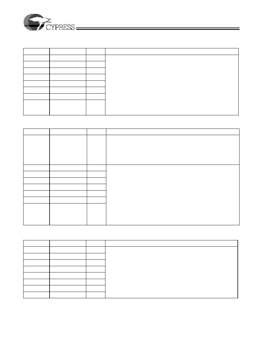
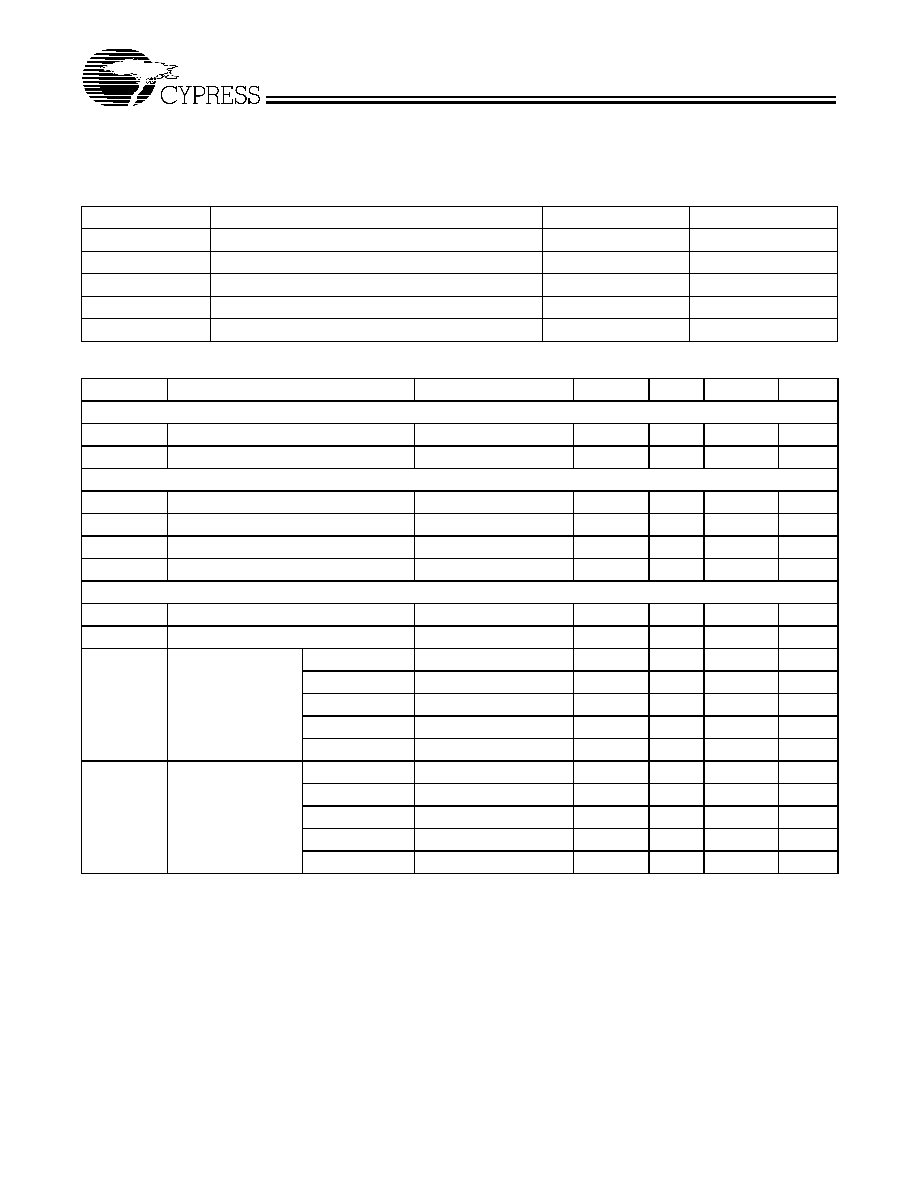
Layout Diagram
G = VIA to GND plane layer V =VIA to respective supply plane layer
Note: Each supply plane or strip should have a ferrite bead and capacitors
G
FB
+3.3V Supply
C4
Ceramic Caps C3 = 10≠22
µ
F C4 = 0.005
µ
F
10
µ
F
FB = Dale ILB1206 - 300 (300
@ 100 MHz) or TDK ACB2012L-120
0.005
µ
F
G
G
V
DDQ3
C3
C6 = 0.01
µ
F
48
47
46
45
44
43
42
41
40
38
37
36
35
34
33
32
31
30
29
28
27
26
25
1
2
3
4
5
6
7
8
9
10
11
12
13
14
15
16
17
18
19
20
21
22
23
24
39
G
V
CY28316
G
V
G
V
G
V
G
V
G
V
G
V
Core
V
DDQ3
G
G
G
G
G
G
G
G
G
G
G
G
G
G
G
G
G
G
G
G
V
G
G
G
FB
+2.5V Supply
C4
10
µ
F
0.005
µ
F
G
G
C3

CY28316
Document #: 38-07125 Rev. **
Page 19 of 20
© Cypress Semiconductor Corporation, 2001. The information contained herein is subject to change without notice. Cypress Semiconductor Corporation assumes no responsibility for the use
of any circuitry other than circuitry embodied in a Cypress Semiconductor product. Nor does it convey or imply any license under patent or other rights. Cypress Semiconductor does not authorize
its products for use as critical components in life-support systems where a malfunction or failure may reasonably be expected to result in significant injury to the user. The inclusion of Cypress
Semiconductor products in life-support systems application implies that the manufacturer assumes all risk of such use and in doing so indemnifies Cypress Semiconductor against all charges.
Package Diagram
48-Pin Small Shrink Outline Package (SSOP, 300 mils)
Summary of nominal dimensions in inches:
Body Width: 0.296
Lead Pitch: 0.025
Body Length: 0.625
Body Height: 0.102

CY28316
Document #: 38-07125 Rev. **
Page 20 of 20
Revision History
Document Title: CY28316 FTG for VIA PL133T and PLE133T
Document Number: 38-07125
REV.
ECN NO.
Issue
Date
Orig. of
Change
Description of Change
**
109866
11/13/01
IKA
New data sheet