/home/web/doc/html/cypress/169285
FTG for VIA PL133T and PLE133T
CY28316
Cypress Semiconductor Corporation
·
3901 North First Street
·
San Jose
,
CA 95134
·
408-943-2600
Document #: 38-07125 Rev. *B
Revised December 14, 2002
Features
· Single-chip system frequency synthesizer for VIA
PL133T and PLE133T chipsets
· Programmable clock output frequency with less than
1 MHz increment
· Integrated fail-safe Watchdog Timer for system
recovery
· Automatically switches to HW-selected or
SW-programmed clock frequency when Watchdog
Timer time-out occurs
· Capable of generating system RESET after a Watchdog
Timer time-out occurs or a change in output frequency
via SMBus interface
· Supports SMBus byte Read/Write and block Read/Write
operations to simplify system BIOS development
· Vendor ID and Revision ID support
· Programmable drive strength for SDRAM and PCI
output clocks
· Programmable output skew for CPU, PCI, and SDRAM
· Maximized electromagnetic interference (EMI)
suppression using Cypress's Spread Spectrum
technology
· Available in 48-pin SSOP
Key Specifications
CPU to CPU Output Skew: ......................................... 175 ps
PCI to PCI Output Skew: ............................................ 500 ps
Note:
1.
Signals marked with `*' have internal pull-up resistors.
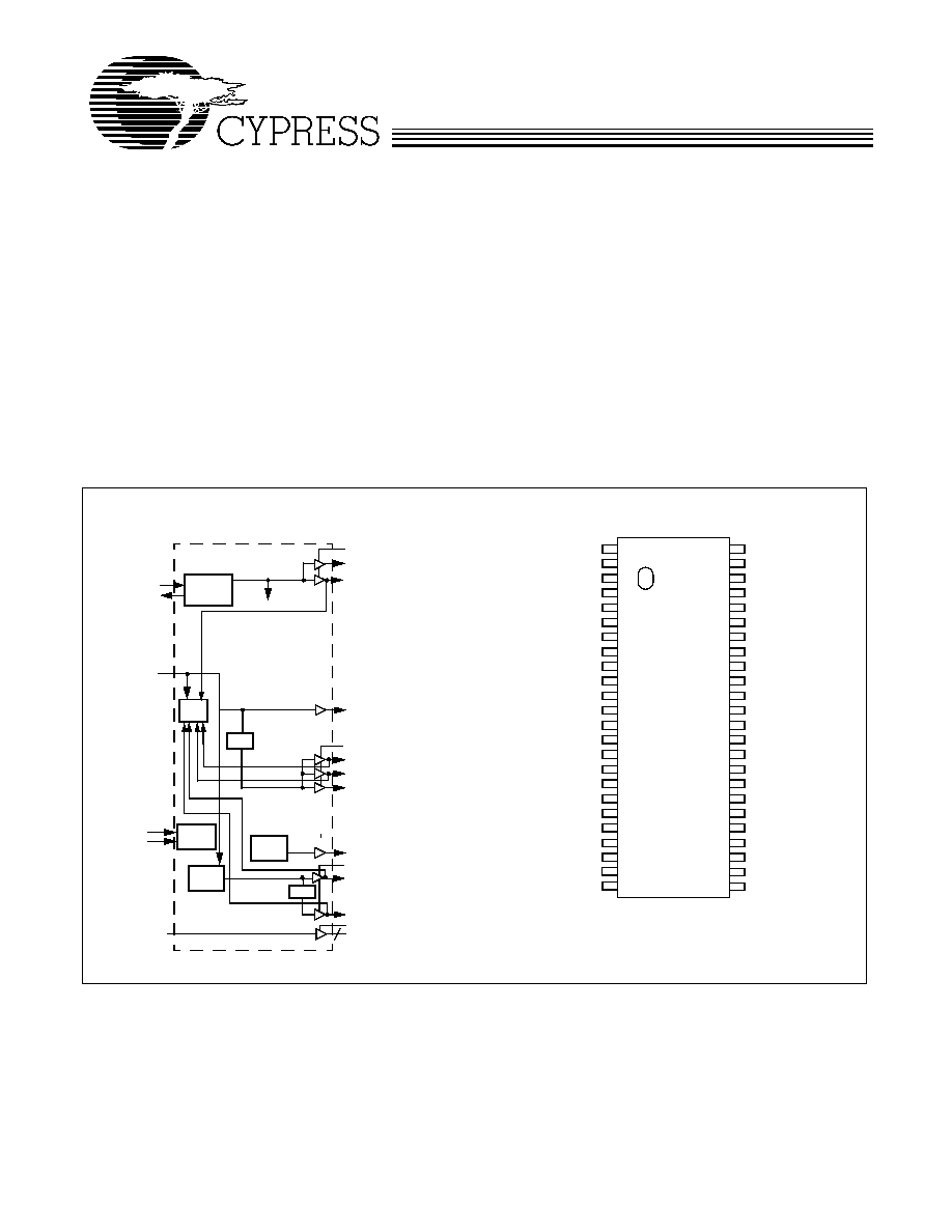
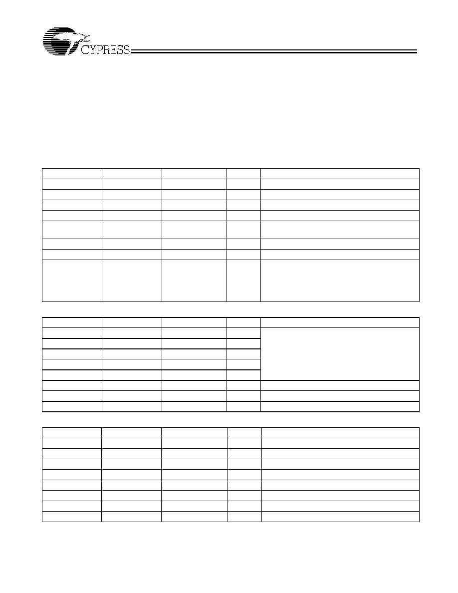
Block Diagram
Pin Configuration
[1]
VDD_REF
REF0
PCI0/FS4*
XTAL
PLL Ref Freq
PLL 1
X2
X1
REF1/FS2*
VDD_PCI
PCI2:6
48MHz/FS0*
24_48MHz/FS1*
PLL2
÷2,3,4
OSC
VTTPWRGD#
VDD_48MHz
SMBus
SDATA
Logic
SCLK
SDRAM0:12
SDRAMIN
13
VDD_SDRAM
PCI1/FS3*
CPU0:1
÷2
VDD_REF
GND_REF
X1
X2
VDD_PCI
*FS4/PCI0
*FS3/PCI1
GND_PCI
PCI2
PCI3
PCI4
PCI5
PCI6
VDD_PCI
SDRAMIN
GND_SDRAM
SDRAM11
SDRAM10
VDD_SDRAM
SDRAM9
SDRAM8
GND_SDRAM
SDATA
SCLK
CY
28
31
6
VTT_PWRGD#
REF0
REF1/FS2*
GND_CPU
CPU0
CPU1
VDD_CPU
RST#
SDRAM_12
GND_SDRAM
SDRAM0
SDRAM1
VDD_SDRAM
SDRAM2
SDRAM3
GND_SDRAM
SDRAM4
SDRAM5
VDD_SDRAM
SDRAM6
SDRAM7
VDD_48MHz
48MHz/FS0*
24_48MHz/FS1*
48
47
46
45
44
43
42
41
40
39
38
37
36
35
34
33
32
31
30
29
28
27
26
25
1
2
3
4
5
6
7
8
9
10
11
12
13
14
15
16
17
18
19
20
21
22
23
24
SMBus
{
Logic
Reset
RST#
CY28316
Document #: 38-07125 Rev. *B
Page 2 of 18
Pin Definitions
Pin Name
Pin No.
Pin Type
Pin Description
CPU0:1
44, 43
O
CPU Clock Output 0 through 1: CPU clocks for processor and chipset.
PCI2:6
9, 10, 11, 12,
13
O
PCI Clock Outputs 2 through 6: 3.3V 33-MHz PCI clock outputs. Frequency is
set by FS0:4 inputs or through serial data interface.
PCI1/FS3
7
I/O
Fixed PCI Clock Output/Frequency Select 3: 3.3V PCI clock outputs. As an
output, frequency is set by FS0:4 inputs or through the serial data interface. This
pin also serves as a power-on strap option to determine the device operating
frequency, as described in Table 5.
PCI0/FS4
6
I/O
Fixed PCI Clock Output/Frequency Select 4: 3.3V PCI clock outputs. This pin
also serves as a power-on strap option to determine the device operating
frequency, as described in Table 5.
RST#
41
O
(open-drain)
Reset# Output: Open drain system reset output.
48MHz/FS0
26
I/O
48-MHz Output/Frequency Select 0: 3.3V 48-MHz non-spread spectrum output.
This pin also serves as a power-on strap option to determine the device operating
frequency as described in Table 5.
24_48MHz/
FS1
25
I/O
24_48MHz Output/Frequency Select 1: 3.3V 24- or 48-MHz non-spread
spectrum output. This pin also serves as a power-on strap option to determine the
device operating frequency, as described in Table 5.
REF1/FS2
46
I/O
Reference Clock Output 1/Frequency Select 2: 3.3V 14.318-MHz output clock.
This pin also serves as a power-on strap option to determine the device operating
frequency as described in Table 5.
REF0
47
O
Reference Clock Output 0: 3.3V 14.318-MHz output clock.
SDRAMIN
15
I
SDRAM Buffer Input Pin: Reference input for SDRAM buffer.
SDRAM0:12
38, 37, 35, 34,
32, 31, 29, 28,
21, 20, 18, 17,
40
O
SDRAM Outputs: These thirteen dedicated outputs provide copies of the signal
provided at the SDRAMIN input.
SCLK
24
I
Clock pin for SMBus circuitry.
SDATA
23
I/O
Data pin for SMBus circuitry.
X1
3
I
Crystal Connection or External Reference Frequency Input: This pin has dual
functions. It can be used as an external 14.318-MHz crystal connection or as an
external reference frequency input.
X2
4
O
Crystal Connection: An output connection for an external 14.318-MHz crystal. If
using an external reference, this pin must be left unconnected.
VTT_PWRGD#
48
I
VTT_PWRGD#: 3.3V LVTTL compatible input that controls the FS0:4 to be latched
and enables all outputs. CY28316 will sample the FS0:4 inputs and enable all clock
outputs after all V
DD
become valid and VTT_PWRGD# is held LOW.
VDD_REF,
VDD_PCI,
VDD_SDRAM,
VDD_48MHz
1, 5, 14, 19,
27, 30, 36
P
Power Connection: Power supply for core logic, PLL circuitry, SDRAM outputs,
PCI outputs, reference outputs, 48-MHz output, and 24_48-MHz output. Connect
to 3.3V supply.
VDD_CPU
42
P
Power Connection: Power supply for CPU outputs. Connect to 2.5V supply.
GND_REF,
GND_PCI,
GND_SDRAM,
VDD_48MHz,
VDD_CPU
2, 8, 16, 22,
33, 39, 45
G
Ground Connections: Connect all ground pins to the common system ground
plane.
CY28316
Document #: 38-07125 Rev. *B
Page 3 of 18
Serial Data Interface
The CY28316 features a two-pin, serial data interface that can
be used to configure internal register settings that control
particular device functions.
Data Protocol
The clock driver serial protocol supports byte/word Write,
byte/word Read, block Write and block Read operations from
the controller. For block Write/Read operation, the bytes must
be accessed in sequential order from lowest to highest byte,
with the ability to stop after any complete byte has been trans-
ferred. For byte/word Write and byte Read operations, the
system controller can access individual indexed bytes. The
offset of the indexed byte is encoded in the command code.
The definition for the command code is defined in Table 1.
Table 1. Command Code Definition
Bit
Descriptions
7
0 = Block read or block write operation
1 = Byte/Word read or byte/word write operation
6:0
Byte offset for byte/word read or write operation. For block read or write operations, these bits
need to be set at `0000000.'
Table 2. Block Read and Block Write Protocol
Block Write Protocol
Block Read Protocol
Bit
Description
Bit
Description
1
Start
1
Start
2:8
Slave address 7 bits
2:8
Slave address 7 bits
9
Write
9
Write
10
Acknowledge from slave
10
Acknowledge from slave
11:18
Command Code 8 bits
`00000000' stands for block operation
11:18
Command Code 8 bits
`00000000' stands for block operation
19
Acknowledge from slave
19
Acknowledge from slave
20:27
Byte Count 8 bits
20
Repeat start
28
Acknowledge from slave
21:27
Slave address 7 bits
29:36
Data byte 0 8 bits
28
Read
37
Acknowledge from slave
29
Acknowledge from slave
38:45
Data byte 1 8 bits
30:37
Byte count from slave 8 bits
46
Acknowledge from slave
38
Acknowledge
...
Data Byte N/Slave Acknowledge...
39:46
Data byte from slave 8 bits
...
Data Byte N 8 bits
47
Acknowledge
...
Acknowledge from slave
48:55
Data byte from slave 8 bits
...
Stop
56
Acknowledge
...
Data bytes from slave/Acknowledge
...
Data byte N from slave 8 bits
...
Not acknowledge
...
Stop
Table 3. Word Read and Word Write Protocol
Word Write Protocol
Word Read Protocol
Bit
Description
Bit
Description
1
Start
1
Start
2:8
Slave address 7 bits
2:8
Slave address 7 bits
9
Write
9
Write
10
Acknowledge from slave
10
Acknowledge from slave
CY28316
Document #: 38-07125 Rev. *B
Page 4 of 18
11:18
Command Code 8 bits
`1xxxxxxx' stands for byte or word operation
bit[6:0] of the command code represents the offset
of the byte to be accessed
11:18
Command Code 8 bits
`1xxxxxxx' stands for byte or word operation
bit[6:0] of the command code represents the offset
of the byte to be accessed
19
Acknowledge from slave
19
Acknowledge from slave
20:27
Data byte low 8 bits
20
Repeat start
28
Acknowledge from slave
21:27
Slave address 7 bits
29:36
Data byte high 8 bits
28
Read
37
Acknowledge from slave
29
Acknowledge from slave
38
Stop
30:37
Data byte low from slave 8 bits
38
Acknowledge
39:46
Data byte high from slave 8 bits
47
Not acknowledge
48
Stop
Table 4. Byte Read and Byte Write Protocol
Byte Write Protocol
Byte Read Protocol
Bit
Description
Bit
Description
1
Start
1
Start
2:8
Slave address 7 bits
2:8
Slave address 7 bits
9
Write
9
Write
10
Acknowledge from slave
10
Acknowledge from slave
11:18
Command Code 8 bits
`1xxxxxxx' stands for byte operation
bit[6:0] of the command code represents the offset
of the byte to be accessed
11:18
Command Code 8 bits
`1xxxxxxx' stands for byte operation
bit[6:0] of the command code represents the offset
of the byte to be accessed
19
Acknowledge from slave
19
Acknowledge from slave
20:27
Data byte 8 bits
20
Repeat start
28
Acknowledge from slave
21:27
Slave address 7 bits
29
Stop
28
Read
29
Acknowledge from slave
30:37
Data byte from slave 8 bits
38
Not acknowledge
39
Stop
Table 3. Word Read and Word Write Protocol (continued)
Word Write Protocol
Word Read Protocol
Bit
Description
Bit
Description
CY28316
Document #: 38-07125 Rev. *B
Page 5 of 18
CY28316 Serial Configuration Map
1. The serial bits will be read by the clock driver in the following
order:
Byte 0 Bits 7, 6, 5, 4, 3, 2, 1, 0
Byte 1 Bits 7, 6, 5, 4, 3, 2, 1, 0
Byte N Bits 7, 6, 5, 4, 3, 2, 1, 0
2. All unused register bits (reserved and N/A) should be writ-
ten to a "0" level.
3. All register bits labeled "Write with 1" must be written to "1"
during initialization.
Byte 0: Control Register 0
Bit
Pin#
Name
Default
Description
Bit 7
Spread Select1
0
See definition in Bit[0].
Bit 6
SEL2
0
See Table 5.
Bit 5
SEL1
0
See Table 5.
Bit 4
SEL0
0
See Table 5.
Bit 3
FS_Override
0
0 = Select operating frequency by FS[4:0] input pins.
1 = Select operating frequency by SEL[4:0] settings.
Bit 2
SEL4
0
See Table 5.
Bit 1
SEL3
0
See Table 5.
Bit 0
Spread Select0
0
`00' = OFF.
`01' = 0.5%.
`10' = ± 0.5%.
`11' = ± 0.25%.
Byte 1: Control Register 1
Bit
Pin#
Name
Default
Description
Bit 7
6
Latched FS4 input
X
Latched FS[4:0] inputs. These bits are read-only.
Bit 6
7
Latched FS3 input
X
Bit 5
46
Latched FS2 input
X
Bit 4
25
Latched FS1 input
X
Bit 3
26
Latched FS0 input
X
Bit 2
44
CPU0
1
(Active/Inactive).
Bit 1
43
CPU1
1
(Active/Inactive).
Bit 0
Vendor Test Mode
1
Write with `1.'
Byte 2: Control Register 2
Bit
Pin#
Name
Default
Description
Bit 7
40
SDRAM12
1
(Active/Inactive).
Bit 6
6
PCI0
1
(Active/Inactive).
Bit 5
13
PCI6
1
(Active/Inactive).
Bit 4
12
PCI5
1
(Active/Inactive).
Bit 3
11
PCI4
1
(Active/Inactive).
Bit 2
10
PCI3
1
(Active/Inactive).
Bit 1
9
PCI2
1
(Active/Inactive).
Bit 0
7
PCI1
1
(Active/Inactive).