PRELIMINARY
133-MHz Spread Spectrum Clock Synthesizer with
Differential CPU Outputs
CY28322-2
Cypress Semiconductor Corporation
∑
3901 North First Street
∑
San Jose
∑
CA 95134
∑
408-943-2600
Document #: 38-07145 Rev. *B
Revised December 14, 2002
Features
Benefits
∑ Compliant with Intel
CK-Titan and CK-408 clock
synthesizer/driver specifications
Supports next generation Pentium
processors using
differential clock drivers
∑ Multiple output clocks at different frequencies
-- Two pairs of differential CPU outputs, up to 200 MHz
-- Nine synchronous PCI clocks, three free-running
-- Six 3V66 clocks
-- Two 48-MHz clocks
-- One reference clock at 14.318 MHz
-- One VCH clock
Motherboard clock generator
-- Support multiple CPUs and a chipset
-- Support for PCI slots and chipset
-- Supports AGP, DRCG reference, and Hub Link
-- Supports USB host and graphic controllers
-- Supports ISA slots and I/O chip
∑ Spread Spectrum clocking (down spread)
Enables reduction of EMI and overall system cost
∑ Power-down features (PCI_STOP#, CPU_STOP#
PWR_DWN#)
Enables ACPI-compliant designs
∑ Two select inputs (Mode select & IC Frequency Select) Supports up to four CPU clock frequencies
∑ 48-pin TSSOP package
Widely available, standard package enables lower cost
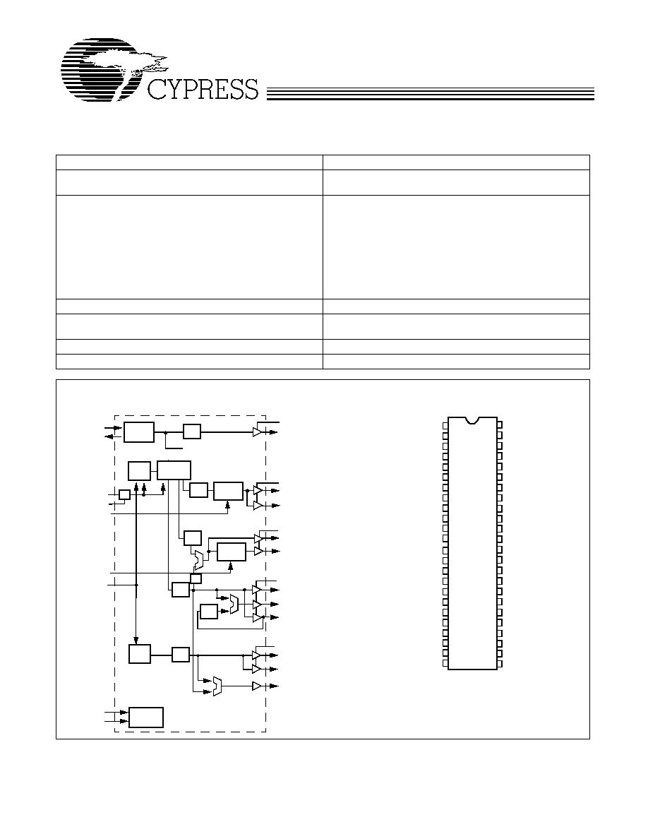
Logic Block Diagram
TSSOP
Top View
1
2
3
4
5
6
7
8
9
10
11
12
25
28
27
XTAL_IN
26
13
14
15
16
17
18
19
20
21
22
23
24
37
36
35
34
33
29
30
31
32
40
39
38
XTAL_OUT
GND_REF
PCI_F0
41
44
43
42
45
48
47
46
PCI2
66BUFF0/3V66_2
GND_CORE
SCLK
GND_48 MHz
CPU2
CPU_STOP#
GND_PCI
VDD_3V66
66IN/3V66_5
3V66_0
USB
CPU#1
VDD_REF
PCI_F1
PCI_F2
PCI0
PCI1
VDD_PCI
PCI3
PCI4
PCI5
GND_3V66
66BUFF1/3V66_3
66BUFF2/3V66_4
PWR_DWN#
VDD_CORE
PWR_GD#
SDATA
GND_3V66
VDD_3V66
PCI_STOP#
3V66_1/VCH
VDD_48 MHz
DOT
S2
IREF
CPU#2
VDD_CPU
GND_CPU
CPU1
VDD_CPU
S1
REF0
C
Y
28
322
-2
VDD_REF
CPU1:2
CPU#1:2
PCI_F0:2
XTAL
PLL Ref Freq
X2
X1
REF
VDD_PCI
USB (48MHz)
VCH_CLK/ 3V66_1
OSC
VDD_CPU
CPU_STOP#
SCLK
PCI0:5
PCI_STOP#
Stop
Clock
Control
Stop
Clock
Control
PLL 1
SMBus
Logic
DOT (48MHz)
PWR_DWN#
S1:2
VDD_48MHz
SDATA
VDD_3V66
3V66_0:1
3V66_2:4/
Divider
Network
3V66_5/ 66IN
PWR
PWR
PWR
PWR
PWR
PLL 2
PWR
66BUFF0:2
Gate
PWR_GD#
Pin Configurations
/2
PRELIMINARY
CY28322-2
Document #: 38-07145 Rev. *B
Page 2 of 17
Pin Summary
Pin Name
Pin Number
Pin Description
REF0
47
3.3V 14.318-MHz clock output
XTAL_IN
1
14.318-MHz crystal input
XTAL_OUT
2
14.318-MHz crystal input
CPU, CPU# [1:2]
43, 39, 42, 38
Differential CPU clock outputs
3V66_0
29
3.3V 66-MHz clock output
3V66_1/VCH
31
3.3V selectable through SMBus to be 66 MHz or 48 MHz
66IN/3V66_5
20
66-MHz input to buffered 66BUFF and PCI or 66-MHz clock from internal VCO
66BUFF [2:0] /3V66 [4:2] 17, 18, 19
66-MHz buffered outputs from 66Input or 66-MHz clocks from internal VCO
PCI_F [0:2]
4, 5, 6
33 MHz clocks divided down from 66Input or divided down from 3V66
PCI [0:5]
8, 9, 10, 12, 13, 14 PCI clock outputs divided down from 66Input or divided down from 3V66
USB
35
Fixed 48-MHz clock output
DOT
34
Fixed 48-MHz clock output
S2
36
Special 3.3V 3-level input for Mode selection
S1
46
3.3V LVTTL inputs for CPU frequency selection
IREF
37
A precision resistor is attached to this pin which is connected to the internal
current reference
PWR_DWN#
21
3.3V LVTTL input for Power_Down# (active LOW)
PCI_STOP#
30
3.3V LVTTL input for PCI_STOP# (active LOW)
CPU_STOP#
45
3.3V LVTTL input for CPU_STOP# (active LOW)
PWRGD#
24
3.3V LVTTL input is a level sensitive strobe used to determine when S[2:1] inputs
are valid and OK to be sampled (Active LOW). Once PWRGD# is sampled LOW,
the status of this output will be ignored.
SDATA
25
SMBus compatible SDATA
SCLK
26
SMBus compatible Sclk
VDD_PCI, VDD_3V66,
VDD_CPU,VDD_REF
11, 15, 28, 40, 44,
48
3.3V power supply for outputs
VDD_48 MHz
33
3.3V power supply for 48 MHz
VDD_CORE
22
3.3V power supply for PLL
GND_REF, GND_PCI,
GND_3V66, GND_IREF,
GND_CPU
3, 7, 16, 27, 32, 41 Ground for outputs
GND_CORE
23
Ground for PLL
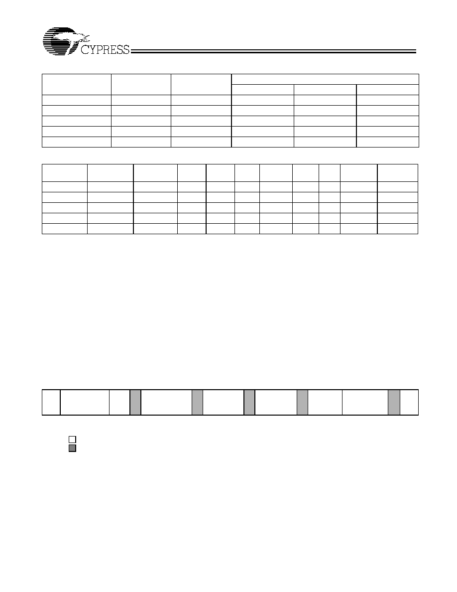
Function Table
[1]
S2
S1 CPU (MHz)
3V66[0:1]
(MHz)
66BUFF[0:2]/3
V66[2:4] (MHz)
66IN/3V66_5
(MHz)
PCI_F/PCI
(MHz)
REF0(MHz)
USB/DOT
(MHz)
Notes
1
0
100 MHz
66 MHz
66IN
66 MHz Input
66IN/2
14.318 MHz
48 MHz
2, 3, 4
1
1
133 MHz
66 MHz
66IN
66 MHz Input
66IN/2
14.318 MHz
48 MHz
2, 3, 4
0
0
100 MHz
66 MHz
66 MHz
66 MHz
33 MHz
14.318 MHz
48 MHz
2, 3, 4
0
1
133 MHz
66 MHz
66 MHz
66 MHz
33 MHz
14.318 MHz
48 MHz
2, 3, 4
Mid
0
TCLK/2
TCLK/4
TCLK/4
TCLK/4
TCLK/8
TCLK
TCLK/2
7, 8, 5
Mid
1
Reserved
Reserved
Reserved
Reserved
Reserved
Reserved
Reserved
≠
Notes:
1.
TCLK is a test clock driven in on the XTALIN input in test mode.
2.
"Normal" mode of operation
3.
Range of reference frequency allowed is min. = 14.316 nominal = 14.31818 MHz, max = 14.32 MHz.
4.
Frequency accuracy of 48 MHz must be +167 PPM to match USB default.
5.
Mid is defined a voltage level between 1.0V and 1.8V for 3 level input functionality. Low is below 0.8V. High is above 2.0V.
6.
Required for DC output impedance verification.
7.
These modes are to use the same internal dividers as the CPU = 200-MHz mode. The only change is to slow down the internal VCO to allow under clock
margining.
8.
All parameters specified with loaded outputs.
PRELIMINARY
CY28322-2
Document #: 38-07145 Rev. *B
Page 3 of 17
Serial Data Interface (SMBus)
To enhance the flexibility and function of the clock synthesizer,
a two signal SMBus interface is provided according to SMBus
specification. Through the Serial Data Interface, various
device functions such as individual clock output buffers, can
be individually enabled or disabled. CY28322-2 supports both
block read and block write operations.
The registers associated with the Serial Data Interface
initialize to their default setting upon power-up, and therefore
use of this interface is optional. Clock device register changes
are normally made upon system initialization, if any are
required. The interface can also be used during system
operation for power management functions.
Data Protocol
The clock driver serial protocol accepts only block writes from
the controller. The bytes must be accessed in sequential order
from lowest to highest byte, (most significant bit first) with the
ability to stop after any complete byte has been transferred.
Indexed bytes are not allowed.
A block write begins with a slave address and a WRITE
condition. The R/W bit is used by the SMBus controller as a
data direction bit. A zero indicates a WRITE condition to the
clock device. The slave receiver address is 11010010 (D2h).
A command code of 0000 0000 (00h) and the byte count bytes
are required for any transfer. After the command code, the
core logic issues a byte count which describes number of
additional bytes required for the transfer, not including the
command code and byte count bytes. For example, if the host
has 20 data bytes to send, the first byte would be the number
20 (14h), followed by the 20 bytes of data. The byte count byte
is required to be a minimum of 1 byte and a maximum of 32
bytes It may not be 0. Figure 1 shows an example of a block
write.
A transfer is considered valid after the acknowledge bit corre-
sponding to the byte count is read by the controller.
Clock Driver Impedances
Buffer
V
DD
Range
Buffer Type
Impedance
Min.
Typ.
Max.
CPU, CPU#
Type X1
50
REF
3.135≠3.465
Type 3
20
40
60
PCI, 3V66, 66BUFF
3.135≠3.465
Type 5
12
30
55
USB
3.135≠3.465
Type 3A
12
30
55
DOT
3.135≠3.465
Type 3B
12
30
55
Clock Enable Configuration
PWR_DWN# CPU_STOP#
PCI_STOP#
CPU
CPU#
3V66
66BUFF
PCI_F
PCI
USB/DOT
VCOS/
OSC
0
X
X
IREF*2
FLOAT
LOW
LOW
LOW
LOW
LOW
OFF
1
0
0
IREF*2
FLOAT
ON
ON
ON
OFF
ON
ON
1
0
1
IREF*2
FLOAT
ON
ON
ON
ON
ON
ON
1
1
0
ON
ON
ON
ON
ON
OFF
ON
ON
1
1
1
ON
ON
ON
ON
ON
ON
ON
ON
Start
Bit
Slave Address
1 1 0 1 0 0 1 0
R/W
0/1
A
Command
Code
0 0 0 0 0 0 0 0
A Byte Count =
N
A
Data Byte 0
A
. . .
Data Byte N-1 A Stop
Bit
1 bit
7 bits
1
1
8 bits
1
8 bits
1
8 bits
1
8 bits
1
1 bit
Figure 1. An Example of a Block Write
From Master to Slave
From Slave to Master
PRELIMINARY
CY28322-2
Document #: 38-07145 Rev. *B
Page 4 of 17
Data Byte Configuration Map
Data Byte 0: Control Register (0 = Enable, 1 = Disable)
Bit
Affected
Pin#
Name
Description
Type
Power-on
Default
Bit 7
4, 5, 6, 10,
11, 12, 13,
16, 17, 18,
33, 35
PCI [0:6]
CPU[2:1]
3V66[1:0]
Spread Spectrum Enable
0 = Spread Off, 1 = Spread On
R/W
0
Bit 6
≠
TBD
TBD
R
0
Bit 5
31
3V66_1/VCH
VCH Select 66 MHz/48 MHz
0 = 66 MHz, 1 = 48 MHz
R/W
0
Bit 4
39, 43, 38,
42
CPU [2:1]
CPU# [2:1]
CPU_STOP#
Reflects the current value of the external CPU_STOP# pin
R
N/A
Bit 3
8, 9, 10, 11,
12, 13, 14,
PCI [5:0]
PCI_STOP#
(Does not affect PCI_F [2:0] pins)
R/W
N/A
Bit 2
≠
≠
S2≠Reflects the value of the S2 pin sampled on power-up
R
N/A
Bit 1
≠
≠
S1≠Reflects the value of the S1 pin sampled on power-up
R
N/A
Bit 0
≠
≠
Reserved
R
1
Data Byte 1
Bit
Pin#
Name
Description
Type
Power-on
Default
Bit 7
≠
N/A
CPU Mult0 Value
R
N/A
Bit 6
43,39,
CPU1:2
Three-state CPU1:2 during power-down
0 = Normal; 1 = Three-stated
R/W
0
Bit 5
38, 39
CPU2
CPU2#
Allow Control of CPU2 with assertion of CPU_STOP#
0 = Not free running; 1 = Free running
R/W
0
Bit 4
42, 43
CPU1
CPU1#
Allow Control of CPU1 with assertion of CPU_STOP#
0 = Not free running;1 = Free running
R/W
0
Bit 3
≠
Reserved
Reserved
R/W
0
Bit 2
38, 39
CPU2
CPU2#
CPU2 Output Enable
1 = Enabled; 0 = Disabled
R/W
1
Bit 1
42, 43
CPU1
CPU1#
CPU1Output Enable
1 = Enabled; 0 = Disabled
R/W
1
Bit 0
≠
Reserved
Reserved
R/W
1
Data Byte 2
Bit
Pin#
Name
Pin Description
Type
Power-on
Default
Bit 7
N/A
N/A
R
0
Bit 6
14
PCI5
PCI5 Output Enable
1 = Enabled, 0 = Disabled
R/W
1
Bit 5
13
PCI4
PCI4 Output Enable
1 = Enabled; 0 = Disabled
R/W
1
Bit 4
12
PCI3
PCI3 Output Enable
1 = Enabled; 0 = Disabled
R/W
1
Bit 3
10
PCI2
PCI2Output Enable
1 = Enabled; 0 = Disabled
R/W
1
Bit 2
9
PCI1
PCI1 Output Enable
1 = Enabled; 0 = Disabled
R/W
1
Bit 1
8
PCI0
PCI0 Output Enable
1 = Enabled; 0 = Disabled
R/W
1
Bit 0
Reserved
Write to"0"
R/W
1
PRELIMINARY
CY28322-2
Document #: 38-07145 Rev. *B
Page 5 of 17
Data Byte 3
Bit
Pin#
Name
Pin Description
Type
Power-on
Default
Bit 7
34
DOT
DOT 48-MHz Output Enable
R/W
1
Bit 6
35
USB
USB 48-MHz Output Enable
R/W
1
Bit 5
6
PCI_F2
Allow control of PCI_F2 with assertion of PCI_STOP#
0 = Free running; 1 = Stopped with PCI_STOP#
R/W
0
Bit 4
5
PCI_F1
Allow control of PCI_F1 with assertion of PCI_STOP#
0 = Free running; 1 = Stopped with PCI_STOP#
R/W
0
Bit 3
4
PCI_F0
Allow control of PCI_F0 with assertion of PCI_STOP#
0 = Free running; 1 = Stopped with PCI_STOP#
R/W
0
Bit 2
6
PCI_F2
PCI_F2 Output Enable
R/W
1
Bit 1
5
PCI_F1
PCI_F1Output Enable
R/W
1
Bit 0
4
PCI_F0
PCI_F0 Output Enable
R/W
1
Data Byte 4
Bit
Pin#
Name
Pin Description
Type
Power-on
Default
Bit 7
≠
TBD
N/A
R
0
Bit 6
≠
TBD
N/A
R
0
Bit 5
29
3V66_0
3V66_0 Output Enable
1 = Enabled; 0 = Disabled
R/W
1
Bit 4
31
3V66_1/VCH
3V66_1/VCH Output Enable
1 = Enabled; 0 = Disabled
R/W
1
Bit 3
20
66IN/3V66_5
3V66_5 Output Enable
1 = Enable; 0 = Disable
Note. This bit should be used when pin 24 is configured as 3v66_5 output.
Do not clear this bit when pin 24 is configured as 66IN input.
R/W
1
Bit 2
19
66BUFF2
66-MHz Buffered 2 Output Enable
1 = Enabled; 0 = Disabled
R/W
1
Bit 1
18
66BUFF1
66-MHz Buffered 1 Output Enable
1 = Enabled; 0 = Disabled
R/W
1
Bit 0
17
66BUFF0
66-MHz Buffered 0 Output Enable
1 = Enabled; 0 = Disabled
R/W
1
Data Byte 5
Bit
Pin#
Name
Pin Description
Type
Power-on
Default
Bit 7
N/A
N/A
R
0
Bit 6
N/A
N/A
R
0
Bit 5
66BUFF [2:0]
Tpd 66IN to 66BUFF propagation delay control
R/W
0
Bit 4
66BUFF [2:0]
R/W
0
Bit 3
DOT
DOT edge rate control
R/W
0
Bit 2
DOT
R/W
0
Bit 1
USB
USB edge rate control
R/W
0
Bit 0
USB
R/W
0
Byte 6: Vendor ID
Bit
Description
Type
Power-on
Default
Bit 7
Revision Code Bit 3
R
0
Bit 6
Revision Code Bit 2
R
0
Bit 5
Revision Code Bit 1
R
0