 | ÐлекÑÑоннÑй компоненÑ: CY28323B | СкаÑаÑÑ:  PDF PDF  ZIP ZIP |
Äîêóìåíòàöèÿ è îïèñàíèÿ www.docs.chipfind.ru
FTG for Intel
®
Pentium
®
4 CPU and Chipsets
CY28323B
Cypress Semiconductor Corporation
·
3901 North First Street
·
San Jose
·
CA 95134
·
408-943-2600
Document #: 38-07453 Rev. *B
Revised November 19, 2003
Features
· Compatible to Intel
®
CK-Titan & CK-408 Clock Synthe-
sizer/Driver Specifications
· System frequency synthesizer for Intel Brookdale 845
and Brookdale - G Pentium
®
4 Chipsets
· Programmable clock output frequency with less than
1 MHz increment
· Integrated fail-safe Watchdog timer for system recov-
ery
· Automatically switch to HW selected or SW pro-
grammed clock frequency when Watchdog timer times
out
· Capable of generating system RESET after a Watchdog
timer time-out occurs or a change in output frequency
via SMBus interface
· Support SMBus byte read/write and block read/ write
operations to simplify system BIOS development
· Vendor ID and Revision ID support
· Programmable drive strength support
· Programmable output skew support
· Power management control inputs
· Available in 48-pin SSOP
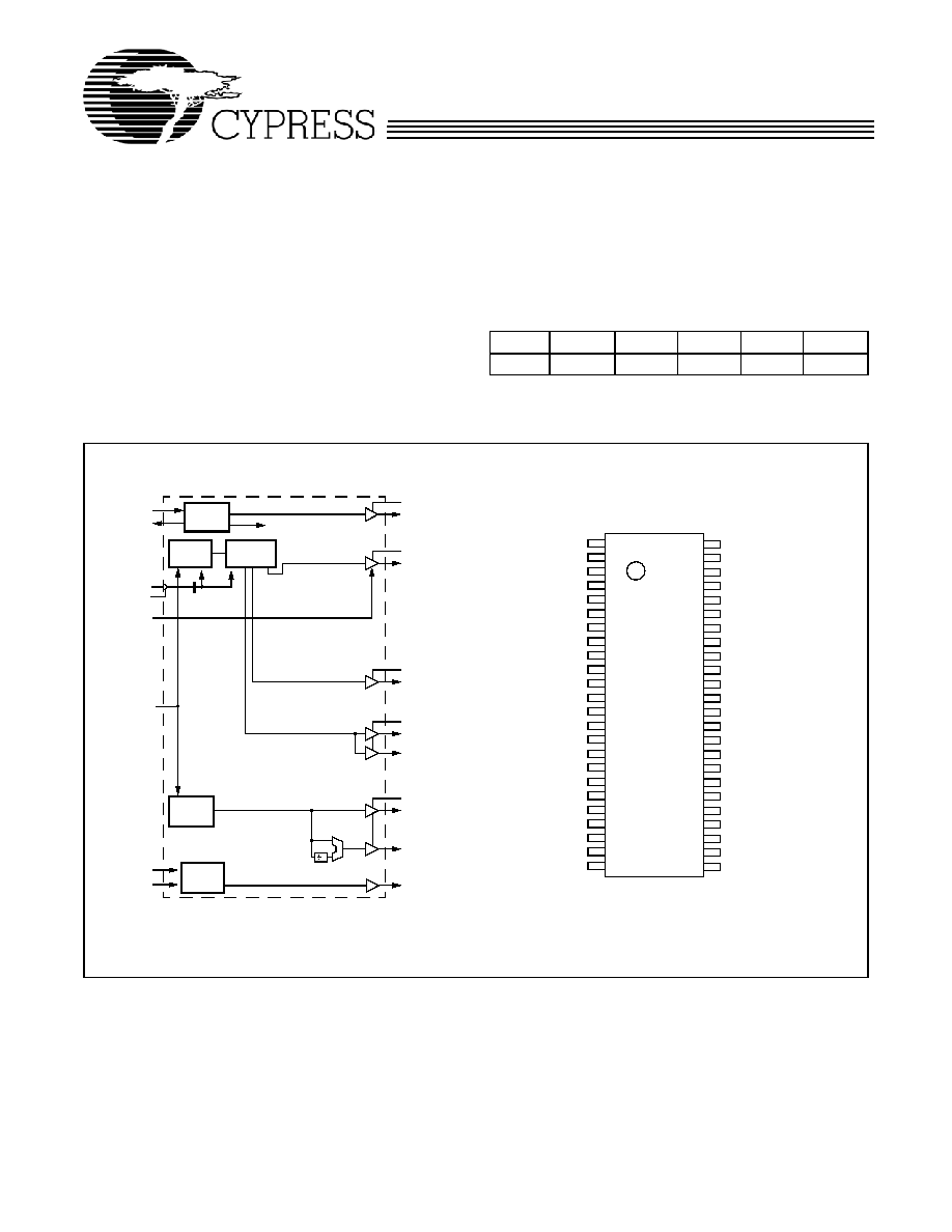
CPU
3V66
PCI
REF
48M
24_48M
x 3
x 4
x 10
x 2
x 1
x 1
Note:
1.
Signals marked with `*' and "^" have internal pull-up and pull-down resistors respectively.
~
Block Diagram
Pin Configuration
VDD_REF
CPU0:1, CPU0:1#,
XTAL
PLL Ref Freq
X2
X1
VDD_PCI
OSC
SCLK
PLL 1
SMBus
Logic
VDD_48MHz
SDATA
VDD_3V66
Divider
Network
VDD_CPU
PLL2
*FS0:4
2
PWR_DWN#
SSOP-48
REF0:1
VTT_PWRGD#
*MULTSEL1/REF1
VDD_REF
X1
X2
GND_PCI
*FS2/PCI_F0
*FS3/PCI_F1
PCI_F2
VDD_PCI
*FS4/PCI0
PCI1
PCI2
GND_PCI
PCI3
PCI4
PCI5
PCI6
VDD_PCI
VTT_PWRGD#
RST#
GND_48MHz
*FS0/48MHz
*FS1/24_48MHz
VDD_48MHz
48
47
46
45
44
43
42
41
40
39
38
37
36
35
34
33
1
2
3
4
5
6
7
8
9
10
11
12
13
14
15
16
17
18
19
20
21
22
23
24
28
27
26
25
32
31
30
29
REF0/MULTSEL0*
GND_REF
VDD_CPU
CPU_ITP
CPU_ITP#
GND_CPU
PWR_DWN#
CPU0
CPU0#
VDD_CPU
CPU1
CPU1#
GND_CPU
IREF
VDD_CORE
GND_CORE
VDD_3V66
3V66_0
3V66_1
GND_3V66
3V66_2
3V66_3
SCLK
SDATA
CY28323B
*MULTSEL0:1
3V66_0:3
PCI_F0:2
PCI0:6
48MHz
24_48MHz
RST#
CPU_ITP, CPU_ITP#
[1]
CY28323B
Document #: 38-07453 Rev. *B
Page 2 of 22
Pin Definitions
Pin Name
Pin No.
Pin
Type
Pin Description
X1
3
I
Crystal Connection or External Reference Frequency Input: This pin has dual
functions. It can be used as an external 14.318-MHz crystal connection or as an
external reference frequency input.
X2
4
O
Crystal Connection: Connection for an external 14.318-MHz crystal. If using an
external reference, this pin must be left unconnected.
REF0/MULTSEL0
48
I/O
Reference Clock 0/Current Multiplier Selection 0: 3.3V 14.318-MHz clock out-
put. This pin also serves as a power-on strap option to determine the current
multiplier for the CPU clock outputs. The MULTSEL1:0 definitions are as follows:
MULTSEL1:0
00 = Ioh is 4 x IREF
01 = Ioh is 5 x IREF
10 = Ioh is 6 x IREF
11 = Ioh is 7 x IREF
REF1/MULTSEL1
1
I/O
Reference Clock 1/Current Multiplier Selection 1: 3.3V 14.318-MHz clock out-
put. This pin also serves as a power-on strap option to determine the current
multiplier for the CPU clock outputs. The MULTSEL1:0 definitions are as follows:
MULTSEL1:0
00 = Ioh is 4 x IREF
01 = Ioh is 5 x IREF
10 = Ioh is 6 x IREF
11 = Ioh is 7 x IREF
CPU0:1, CPU0:1#
41, 38, 40,
37
O
CPU Clock Outputs: Frequency is set by the FS0:4 inputs or through serial input
interface.
CPU_ITP,
CPU_ITP#
44, 45
I/O
CPU Clock Output for ITP: Frequency is set by the FS0:4 inputs or through
serial input interface.
3V66_0:3
31, 30, 28,
27
O
66-MHz Clock Outputs: 3.3V fixed 66-MHz clock.
PCI_F0/FS2
6
I/O
Free-running PCI Output 0/Frequency Select 2: 3.3V free-running PCI output.
This pin also serves as a power-on strap option to determine device operating
frequency as described in the Frequency Selection Table.
PCI_F1/FS3
7
I/O
Free-running PCI Output 1/Frequency Select 3: 3.3V free-running PCI output.
This pin also serves as a power-on strap option to determine device operating
frequency as described in Table 4.
PCI_F2
8
I/O
Free-running PCI Output 2: 3.3V free-running PCI output.
PCI0/FS4
10
I/O
PCI Output 0/Frequency Select 4: 3.3V PCI output. This pin also serves as a
power-on strap option to determine device operating frequency as described in
Table 4.
PCI1:6
11, 12, 14,
15, 16, 17
O
PCI Clock Output 1 to 6: 3.3V PCI clock outputs.
48MHz/FS0
22
I/O
48-MHz Output/Frequency Select 0: 3.3V fixed 48-MHz, non-spread spectrum
output. This pin also serves as a power-on strap option to determine device
operating frequency as described in Table 4.
This output will be used as the reference clock for USB host controller in Intel 845
(Brookdale) platforms. For Intel Brookdale - G platforms, this output will be used
as the VCH reference clock.
CY28323B
Document #: 38-07453 Rev. *B
Page 3 of 22
24_48MHz/FS1
23
I/O
24- or 48-MHz Output/Frequency Select 1: 3.3V fixed 24-MHz or 48-MHz
non-spread spectrum output. This pin also serves as a power-on strap option to
determine device operating frequency as described in Table 4.
This output will be used as the reference clock for SIO devices in Intel 845
(Brookdale) platforms. For Intel Brookdale - G platforms, this output will be used
as the reference clock for both USB host controller and SIO devices. We recom-
mend system designer to configure this output as 48 MHz and "HIGH Drive" by
setting Byte [5], Bit [0] and Byte [9], Bit [7], respectively.
PWR_DWN#
42
I
Power Down Control: 3.3V LVTTL-compatible input that places the device in
power-down mode when held LOW.
SCLK
26
I
SMBus Clock Input: Clock pin for serial interface.
SDATA
25
I/O
SMBus Data Input: Data pin for serial interface.
RST#
20
O
(open-
drain)
System Reset Output: Open-drain system reset output.
IREF
35
I
Current Reference for CPU Output: A precision resistor is attached to this pin
which is connected to the internal current reference.
VTT_PWRGD#
19
I
Powergood from Voltage Regulator Module (VRM): 3.3V LVTTL input.
VTT_PWRGD# is a level-sensitive strobe used to determine when FS0:4 and
MULTSEL0:1 inputs are valid and OK to be sampled (Active LOW). Once
VTT_PWRGD# is sampled LOW, the status of this input will be ignored.
VDD_REF,
VDD _PCI,
VDD_48MHz,
VDD_3V66,
VDD_CPU
2, 9, 18, 24,
32, 39, 46
P
3.3V Power Connection: Power supply for CPU outputs buffers, 3V66 output
buffers, PCI output buffers, reference output buffers and 48-MHz output buffers.
Connect to 3.3V.
GND_PCI,
GND_48MHz,
GND_3V66,
GND_CPU,
GND_REF,
5, 13, 21, 29,
36, 43, 47
G
Ground Connection: Connect all ground pins to the common system ground
plane.
VDD_CORE
34
P
3.3V Analog Power Connection: Power supply for core logic, PLL circuitry.
Connect to 3.3V.
GND_CORE
33
G
Analog Ground Connection: Ground for core logic, PLL circuitry.
Pin Definitions
(continued)
Pin Name
Pin No.
Pin
Type
Pin Description
CY28323B
Document #: 38-07453 Rev. *B
Page 4 of 22
Swing Select Functions
MULTSEL1
MULTSEL0
Board Target
Trace/Term Z
Reference R, IREF
=
VDD/(3*Rr)
Output
Current
V
OH
@ Z
0
0
50
Rr = 221 1%,
IREF = 5.00 mA
I
OH
= 4*Iref
1.0V @ 50
0
0
60
Rr = 221 1%,
IREF = 5.00 mA
I
OH
= 4*Iref
1.2V @ 60
0
1
50
Rr = 221 1%,
IREF = 5.00 mA
I
OH
= 5*Iref
1.25V @ 50
0
1
60
Rr = 221 1%,
IREF = 5.00 mA
I
OH
= 5*Iref
1.5V @ 60
1
0
50
Rr = 221 1%,
IREF = 5.00 mA
I
OH
= 6*Iref
1.5V @ 50
1
0
60
Rr = 221 1%,
IREF = 5.00 mA
I
OH
= 6*Iref
1.8V @ 60
1
1
50
Rr = 221 1%,
IREF = 5.00 mA
I
OH
= 7*Iref
1.75V @ 50
1
1
60
Rr = 221 1%,
IREF = 5.00 mA
I
OH
= 7*Iref
2.1V @ 60
0
0
50
Rr = 475 1%,
IREF = 2.32 mA
I
OH
= 4*Iref
0.47V @ 50
0
0
60
Rr = 475 1%,
IREF = 2.32 mA
I
OH
= 4*Iref
0.56V @ 60
0
1
50
Rr = 475 1%,
IREF = 2.32 mA
I
OH
= 5*Iref
0.58V @ 50
0
1
60
Rr = 475 1%,
IREF = 2.32 mA
I
OH
= 5*Iref
0.7V @ 60
1
0
50
Rr = 475 1%,
IREF = 2.32 mA
I
OH
= 6*Iref
0.7V @ 50
1
0
60
Rr = 475 1%,
IREF = 2.32 mA
I
OH
= 6*Iref
0.84V @ 60
1
1
50
Rr = 475 1%,
IREF = 2.32 mA
I
OH
= 7*Iref
0.81V @ 50
1
1
60
Rr = 475 1%,
IREF = 2.32 mA
I
OH
= 7*Iref
0.97V @ 60
CY28323B
Document #: 38-07453 Rev. *B
Page 5 of 22
Serial Data Interface
To enhance the flexibility and function of the clock synthesizer,
a two-signal serial interface is provided. Through the Serial
Data Interface, various device functions such as individual
clock output buffers, etc. can be individually enabled or dis-
abled.
The register associated with the Serial Data Interface initializ-
es to its default setting upon power-up, and therefore use of
this interface is optional. Clock device register changes are
normally made upon system initialization, if any are required.
The interface can also be used during system operation for
power management functions.
Data Protocol
The clock driver serial protocol accepts byte write, byte read,
block write and block read operation from the controller. For
block write/read operation, the bytes must be accessed in se-
quential order from lowest to highest byte (most significant bit
first) with the ability to stop after any complete byte has been
transferred. For byte write and byte read operations, the sys-
tem controller can access individual indexed bytes. The offset
of the indexed byte is encoded in the command code, as de-
scribed in Table 1.
The block write and block read protocol is outlined in Table 2
while Table 3 outlines the corresponding byte write and byte
read protocol.
The slave receiver address is 11010010 (D2h).
Table 1. Command Code Definition
Bit
Descriptions
7
0 = Block read or block write operation
1 = Byte read or byte write operation
6:0
Byte offset for byte read or byte write operation. For block read or block write operations, these
bits should be `0000000'.
Table 2. Block Read and Block Write Protocol
Block Write Protocol
Block Read Protocol
Bit
Description
Bit
Description
1
Start
1
Start
2:8
Slave address 7 bits
2:8
Slave address 7 bits
9
Write
9
Write
10
Acknowledge from slave
10
Acknowledge from slave
11:18
Command Code 8 bits
`00000000' stands for block operation
11:18
Command Code 8 bits
`00000000' stands for block operation
19
Acknowledge from slave
19
Acknowledge from slave
20:27
Byte Count 8 bits
20
Repeat start
28
Acknowledge from slave
21:27
Slave address 7 bits
29:36
Data byte 0 8 bits
28
Read
37
Acknowledge from slave
29
Acknowledge from slave
38:45
Data byte 1 8 bits
30:37
Byte count from slave 8 bits
46
Acknowledge from slave
38
Acknowledge
...
Data Byte N/Slave Acknowledge...
39:46
Data byte from slave 8 bits
...
Data Byte N 8 bits
47
Acknowledge
...
Acknowledge from slave
48:55
Data byte from slave 8 bits
...
Stop
56
Acknowledge
...
Data bytes from slave/Acknowledge
...
Data byte N from slave 8 bits
...
Not Acknowledge
...
Stop