PRELIMINARY
FTG for Intel
Æ
Pentium
Æ
4 CPU and Chipsets
CY28324
Cypress Semiconductor Corporation
∑
3901 North First Street
∑
San Jose
∑
CA 95134
∑
408-943-2600
Document #: 38-07002 Rev. *A
Revised November 14, 2001
Features
∑ Compatible to Intel
Æ
CK-00, CK-Titan & CK-408 Clock
Synthesizer/Driver Specifications
∑ System frequency synthesizer for Intel 850, Brookdale
(845) and Brookdale - G Pentium
Æ
4 Chipsets
∑ Programmable clock output frequency with less than 1
MHz increment
∑ Integrated fail-safe Watchdog Timer for system
recovery
∑ Automatically switch to HW selected or SW
programmed clock frequency when Watchdog Timer
time-out
∑ Capable of generating system RESET after a Watchdog
Timer time-out occurs or a change in output frequency
via SMBus interface
∑ Support SMBus byte read/write and block read/write
operations to simplify system BIOS development
∑ Vendor ID and Revision ID support
∑ Programmable drive strength support
∑ Programmable output skew support
∑ Power management control inputs
∑ Available in 48-pin SSOP
CPU
3V66
PCI
REF
48M
24_48M
x 2
x 4
x 10
x 2
x 1
x 1
Intel and Pentium are registered trademarks of Intel Corporation.
~
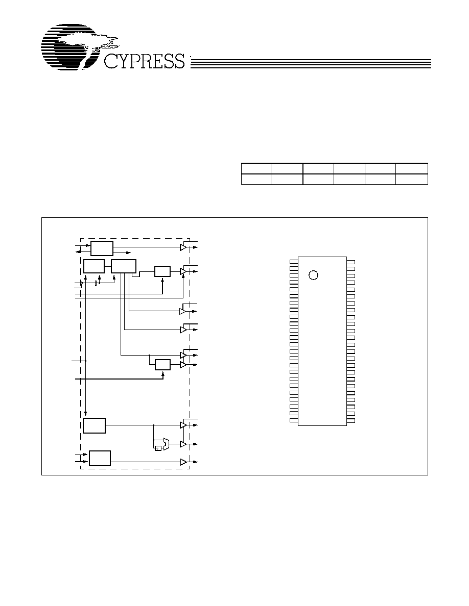
Block Diagram
Pin Configuration
VDD_REF
CPU0:1, CPU0:1#
XTAL
PLL Ref Freq
X2
X1
VDD_PCI
OSC
SCLK
PLL 1
SMBus
Logic
VDD_48MHz
SDATA
VDD_3V66
Divider
Network
VDD_CPU
Stop
Clock
Control
Stop
Clock
Control
PLL2
*FS0:4
2
*CPU_STP#
PWR_DWN#
*PCI_STP#
SSOP-48
REF0:1
VTT_PWRGD#
*MULTSEL1/REF1
VDD_REF
X1
X2
GND_PCI
*FS2/PCI_F0
*FS3/PCI_F1
*MODE/PCI_F2
VDD_PCI
*FS4/PCI0
PCI1
PCI2
GND_PCI
PCI3
PCI4
PCI5
PCI6
VDD_PCI
VTT_PWRGD#
RST#
GND_48MHz
*FS0/48MHz
*FS1/24_48MHz
VDD_48MHz
48
47
46
45
44
43
42
41
40
39
38
37
36
35
34
33
1
2
3
4
5
6
7
8
9
10
11
12
13
14
15
16
17
18
19
20
21
22
23
24
28
27
26
25
32
31
30
29
REF0/MULTSEL0*
GND_REF
VDD_MREF
3VMREF/CPU_STP#*
3VMREF#/PCI_STP#*
GND_MREF
PWR_DWN#
CPU0
CPU0#
VDD_CPU
CPU1
CPU1#
GND_CPU
IREF
VDD_CORE
GND_CORE
VDD_3V66
3V66_0
3V66_1
GND_3V66
3V66_2
3V66_3
SCLK
SDATA
CY
28
32
4
*MULTSEL0:1
3V66_0:3
PCI_F0:2
PCI0:6
48MHz
24_48MHz
RST#
VDD_MREF
3VMREF, 3VMREF#
Note:
1.
Signals marked with `*' have internal pull-up resistor.
PRELIMINARY
CY28324
Document #: 38-07002 Rev. *A
Page 2 of 23
Pin Definitions
Pin Name
Pin No.
Pin
Type
Pin Description
X1
3
I
Crystal Connection or External Reference Frequency Input: This pin has
dual functions. It can be used as an external 14.318-MHz crystal connection
or as an external reference frequency input.
X2
4
O
Crystal Connection: Connection for an external 14.318-MHz crystal. If using
an external reference, this pin must be left unconnected.
REF0/MULTSEL0
48
I/O
Reference Clock 0/Current Multiplier Selection 0: 3.3V 14.318-MHz clock
output. This pin also serves as a power-on strap option to determine the current
multiplier for the CPU clock outputs. The MULTSEL1:0 definitions are as fol-
lows:
MULTSEL1:0
00 = I
OH
is 4 x IREF
01 = I
OH
is 5 x IREF
10 = I
OH
is 6 x IREF
11 = I
OH
is 7 x IREF
REF1/MULTSEL1
1
I/O
Reference Clock 1/Current Multiplier Selection 1: 3.3V 14.318-MHz clock
output. This pin also serves as a power-on strap option to determine the current
multiplier for the CPU clock outputs. The MULTSEL1:0 definitions are as fol-
lows:
MULTSEL1:0
00 = Ioh is 4 x IREF
01 = I
OH
is 5 x IREF
10 = I
OH
is 6 x IREF
11 = I
OH
is 7 x IREF
CPU0:1, CPU0:1#
41, 38, 40, 37
O
CPU Clock Outputs: Frequency is set by the FS0:4 inputs or through the serial
input interface.
3VMREF/CPU_STP
#
45
I/O
Memory Reference Clock/CPU Output Control: The function of this pin is
controlled by the Mode input pin. When Mode input is sampled HIGH during
power-on reset, this pin will be configured as 3VMREF output. When Mode
input is sampled LOW during power-on reset, this pin will be configured as
CPU_STP# input.
3VMREF is a 3.3V output running at half the frequency of the CPU output clock.
CPU_STP# is a 3.3V LVTTL compatible input that disables CPU0, CPU0#,
CPU1 and CPU1# outputs.
3VMREF#/PCI_STP
#
44
I/O
Memory Reference Clock/PCI Output Control: The function of this pin is
controlled by the Mode input pin. When Mode input is sampled HIGH during
power-on reset, this pin will be configured as 3VMREF# output. When Mode
input is sampled LOW during power-on reset, this pin will be configured as
PCI_STP# input.
3VMREF# is a 3.3V output running at half the frequency of the CPU output
clock. 3VMREF# is 180 degree out of phase with respect to 3VMREF.
PCI_STP# is a 3.3V LVTTL-compatible input that disables PCI0:6 outputs.
3V66_0:3
31, 30, 28, 27
O
66-MHz Clock Outputs: 3.3V fixed 66-MHz clock.
PCI_F0/FS2
6
I/O
Free-running PCI Output 0/Frequency Select 2: 3.3V free-running PCI out-
put. This pin also serves as a power-on strap option to determine device op-
erating frequency as described in the Frequency Selection Table.
PCI_F1/FS3
7
I/O
Free-running PCI Output 1/Frequency Select 3: 3.3V free-running PCI out-
put. This pin also serves as a power-on strap option to determine device op-
erating frequency as described in the Frequency Selection Table.
PRELIMINARY
CY28324
Document #: 38-07002 Rev. *A
Page 3 of 23
PCI_F2/Mode
8
I/O
Free-running PCI Output 2/Mode Selection: 3.3V free-running PCI output.
This pin also serves as a power-on strap option to determine the functions of
3VMREF/CPU_STP# and 3VMREF#/PCI_STP#.
When Mode input is sampled HIGH during power-on reset,
3VMREF/CPU_STP# and 3VMREF#/PCI_STP# will be configured as
3VMREF and 3VMREF# output, respectively.
When Mode input is sampled LOW during power-on reset,
3VMREF/CPU_STP# and 3VMREF#/PCI_STP# will be configured as
CPU_STP# and PCI_STP# input, respectively.
PCI0/FS4
10
I/O
PCI Output 0/Frequency Select 4: 3.3V PCI output. This pin also serves as
a power-on strap option to determine device operating frequency as described
in the Frequency Selection Table.
PCI1:6
11, 12, 14, 15,
16, 17
O
PCI Clock Output 1 to 6: 3.3V PCI clock outputs.
48MHz/FS0
22
I/O
48MHz Output/Frequency Select 0: 3.3V fixed 48-MHz, non-spread spec-
trum output. This pin also serves as a power-on strap option to determine
device operating frequency as described in Table 4.
This output will be used as the reference clock for USB host controller in Intel
845 (Brookdale) platforms. For Intel Brookdale - G platforms, this output will
be used as the VCH reference clock.
24_48MHz/FS1
23
I/O
24- or 48-MHz Output/Frequency Select 1: 3.3V fixed 24-MHz or 48-MHz
non-spread spectrum output. This pin also serves as a power-on strap option
to determine device operating frequency as described in Table 4.
This output will be used as the reference clock for SIO devices in Intel 845
(Brookdale) platforms. For Intel Brookdale - G platforms, this output will be
used as the reference clock for both USB host controller and SIO devices. We
recommend system designer to configure this output as 48 MHz and "HIGH
Drive" by setting Byte [5], Bit [0] and Byte [9], Bit [7], respectively.
PWR_DWN#
42
I
Power Down Control: 3.3V LVTTL-compatible input that places the device in
power down mode when held LOW.
SCLK
26
I
SMBus Clock Input: Clock pin for serial interface.
SDATA
25
I/O
SMBus Data Input: Data pin for serial interface.
RST#
20
O
(open-
drain)
System Reset Output: Open-drain system reset output.
IREF
35
I
Current Reference for CPU Output: A precision resistor is attached to this
pin, which is connected to the internal current reference.
VTT_PWRGD#
19
I
Powergood from Voltage Regulator Module (VRM): 3.3V LVTTL input.
VTT_PWRGD# is a level sensitive strobe used to determine when FS0:4,
MODE and MULTSEL0:1 inputs are valid and OK to be sampled (Active LOW).
Once VTT_PWRGD# is sampled LOW, the status of this input will be ignored.
VDD_REF,
VDD _PCI,
VDD_48MHz,
VDD_3V66,
VDD_CPU
VDD_MREF
2, 9, 18, 24,
32, 39, 46
P
3.3V Power Connection: Power supply for CPU outputs buffers, 3V66 output
buffers, PCI output buffers, reference output buffers and 48-MHz output buffers.
Connect to 3.3V.
Pin Definitions
(continued)
Pin Name
Pin No.
Pin
Type
Pin Description
PRELIMINARY
CY28324
Document #: 38-07002 Rev. *A
Page 4 of 23
GND_PCI,
GND_48MHz,
GND_3V66,
GND_CPU,
GND_MREF,
GND_REF,
5, 13, 21, 29,
36, 43, 47
G
Ground Connection: Connect all ground pins to the common system ground
plane.
VDD_CORE
34
P
3.3V Analog Power Connection: Power supply for core logic, PLL circuitry.
Connect to 3.3V.
GND_CORE
33
G
Analog Ground Connection: Ground for core logic, PLL circuitry.
Pin Definitions
(continued)
Pin Name
Pin No.
Pin
Type
Pin Description
PRELIMINARY
CY28324
Document #: 38-07002 Rev. *A
Page 5 of 23
Swing Select Functions
MULTSEL1
MULTSEL0
Board Target
Trace/Term Z
Reference R,
IREF = V
DD
/(3*Rr)
Output
Current
V
OH
@ Z
0
0
50
Rr = 221 1%,
IREF = 5.00 mA
I
OH
= 4*IREF
1.0V @ 50
0
0
60
Rr = 221 1%,
IREF = 5.00 mA
I
OH
= 4*IREF
1.2V @ 60
0
1
50
Rr = 221 1%,
IREF = 5.00 mA
I
OH
= 5*IREF
1.25V @ 50
0
1
60
Rr = 221 1%,
IREF = 5.00 mA
I
OH
= 5*IREF
1.5V @ 60
1
0
50
Rr = 221 1%,
IREF = 5.00 mA
I
OH
= 6*IREF
1.5V @ 50
1
0
60
Rr = 221 1%,
IREF = 5.00 mA
I
OH
= 6*IREF
1.8V @ 60
1
1
50
Rr = 221 1%,
IREF = 5.00 mA
I
OH
= 7*IREF
1.75V @ 50
1
1
60
Rr = 221 1%,
IREF = 5.00 mA
I
OH
= 7*IREF
2.1V @ 60
0
0
50
Rr = 475 1%,
IREF = 2.32 mA
I
OH
= 4*IREF
0.47V @ 50
0
0
60
Rr = 475 1%,
IREF = 2.32 mA
I
OH
= 4*IREF
0.56V @ 60
0
1
50
Rr = 475 1%,
IREF = 2.32 mA
I
OH
= 5*IREF
0.58V @ 50
0
1
60
Rr = 475 1%,
IREF = 2.32 mA
I
OH
= 5*IREF
0.7V @ 60
1
0
50
Rr = 475 1%,
IREF = 2.32 mA
I
OH
= 6*IREF
0.7V @ 50
1
0
60
Rr = 475 1%,
IREF = 2.32 mA
I
OH
= 6*IREF
0.84V @ 60
1
1
50
Rr = 475 1%,
IREF = 2.32 mA
I
OH
= 7*IREF
0.81V @ 50
1
1
60
Rr = 475 1%,
IREF = 2.32 mA
I
OH
= 7*IREF
0.97V @ 60