FTG for VIA PT880 Serial Chipset
CY28326
Cypress Semiconductor Corporation
∑
3901 North First Street
∑
San Jose
,
CA 95134
∑
408-943-2600
Document #: 38-07616 Rev. *A
Revised June 22, 2004
Features
∑ Supports P4
CPUs
∑ 3.3V power supply
∑ Ten copies of PCI clocks
∑ One 48 MHz USB clock
∑ Two copies of 25 MHz for SRC/LAN clocks
∑ One 48 MHz/24 MHz programmable SIO clock
∑ Three differential CPU clock pairs
∑ SMBus support with Byte Write/Block Read/Write
capabilities
∑ Spread Spectrum EMI reduction
∑ Dial-A-Frequency
Æ
features
∑ Auto Ratio features
∑ 48-pin SSOP package
Note:
1.
Pins marked with [*] have internal 150k
pull-up resistors. Pins marked with [**] have internal 150k pull-down resistors.
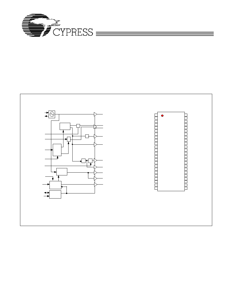
Block Diagram
Pin Configuration
[1]
PLL1
PLL2
/2
WD
Logic
XIN
XOUT
CPU_STP#
IREF
FS[A:D]
VTTPWRGD#
MODE
PD#
SDATA
SCLK
24_48MHz
48MHz
PCI_F[0:2]
PCI[0:6]
AGP[0:2]
REF[0:2]
I2C
Logic
SRESET
Power
on
Latch
CPUC[0:2]
CPUT[0:2]
25MHz[0:1]
PCI_STP#
1
2
3
4
5
6
7
8
9
10
11
12
13
14
15
16
17
18
19
20
21
22
23
24
48
47
46
45
44
43
42
41
40
39
38
37
36
35
34
33
32
31
30
29
28
27
26
25
VDDA
VSSA
IREF
CPUT2
CPUC2
VSSCPU
CPUT1
CPUC1
VDDCPU
CPUT0
CPUC0
VSSSRC
25MHz1
25MHz0
VDDSRC
*VTT_PWRGD/*PD#
SDATA
SCLK
SRESET#
AGP2
VSSAGP
VDDAGP
AGP1/*RatioSel
AGP0
**FSA/REF0
**FSB/REF1
VDDREF
XIN
XOUT
VSSREF
*FSC/PCIF0
*FSD/PCIF1
*Mode/PCIF2
VDDPCI
VSSPCI
PCI0
PCI1
PCI2
PCI4
PCI3
VDDPCI
VSSPCI
*(PCI_STP#)/Ratio0/PCI5
*(CPU_STP#)/Ratio1/PCI6
48MHz
**24_48_SEL/24_48MHz
VSS48
VDD48
C
Y
283
26
48 Pin SSOP
CY28326
Document #: 38-07616 Rev. *A
Page 2 of 23
Pin Definition
Pin No.
Name
PWR
Type
Description
1
**FSA/REF0
VDDREF
I/O
Power-on Bi-directional Input/Output. At power-up, FSA is the
input. when VTT_PWRGD transitions to a logic high, FSA state is
latched and this pin becomes REF0, buffered output copy of the
device's XIN clock. Default Internal pull down.
2
**FSB/REF1
VDDREF
I/O
Power-on Bi-directional Input/Output. At power-up, FSB is the
input. when VTT_PWRGD transitions to a logic high, FSB state is
latched and this pin becomes REF1, buffered output copy of the
device's XIN clock. Default Internal pull down.
3
VDDREF
I
3.3V Power supply for REF clock output.
4
XIN
VDDREF
I
Oscillator Buffer Input. Connect to a crystal or to an external
clock.
5
XOUT
VDDREF
O
Oscillator Buffer Input. Connect to a crystal. Do not connect
when an external clock is applied at XIN.
6
VSSREF
PWR
Ground for REF clock outputs
7
*FSC/PCIF0
VDDPCI
I/O
Power-on Bi-directional Input/ Output. At power up, FSC is the
input. When the VTT_PWRGD transitions to a logic high, FSC
state is latched and this pin becomes PCIF0. Default Internal pull
up.
8
*FSD/PCIF1
VDDPCI
I/O
Power-on Bi-directional Input/ Output. At power up, FSD is the
input. When the VTT_PWRGD transitions to a logic high, FSD
state is latched and this pin becomes PCIF. Default Internal pull
up.
9
*MODE/
PCIF2
VDDPCI
I/O
Power-on Bi-directional Input/ Output. At power up,
MODE/PCIF2 is the input. When the power up, MODE state is
latched and then pin9 becomes PCIF2, PCI clock output for PCI
Device.Default pull-up, See Table 2
10,17
VDDPCI
I
3.3V power supply for PCI clock output.
11,18
VSSPCI
I
Ground for PCI clock output.
12,13,14,15,16
PCI[0:4]
O
PCI clock outputs.
19
*(PCI_STP#)
Ratio0/PCI5
VDDPCI
O
Ratio0 Output/PCI5 Output. At power up when RatioSel (pin 26)
strapping = "High" & MODE (pin 9) strapping="High", (PCI_STP#)
Ratio0/PCI5 becomes PCI5 clock output. At power up when
RatioSel (pin 26) strapping = "low" & MODE (pin 9) strapping
="High", (PCI_STP#)Ratio0/PCI5 becomes Ratio0 output to
support North bridge over freq strapping function. Once
MODE(pin 9) strapping="Low", then (PCI_STP#)Ratio0/PCI5
becomes PCI_STP#, Default = "PCI5" see Table 2, Default
Internal pull up.
20
*(CPU_STP#)
Ratio1/PCI6
VDDPCI
O
Ratio1 Output/PCI6 Output. At power up when RatioSel(pin 26)
strapping = "High" & MODE(pin 9) strapping="High", (CPU_STP#)
Ratio1/PCI6 becomes PCI6 clock output. At power up when
RatioSel (pin 26) strapping = "low" & MODE(pin 9) strapping
="High", (PCI_STP#)Ratio1/PCI6 becomes Ratio1 output to
support North bridge over freq strapping function. Once
MODE(pin 9) strapping="Low", then (PCI_STP#)Ratio1/PCI6
becomes CPU_STP#, Default = "PCI6" see Table 2, Default
Internal pull up.
21
48 MHz
VDD48
O
48 MHz Clock Output.
22
**24_48_SEL/
24_48 MHz
VDD48
I/O
Power-on Bi-directional Input/output. At power up 24_48_SEL
is the input. When VTT_PWRGD is transited to logic high,
24_48_SEL state is latched and this pin becomes 24/48 MHz
output, Default 24_48_SEL= "0", 48 MHz output.Default Internal
pull down.
23
VSS48
I
Ground for 48 MHz clock output.
CY28326
Document #: 38-07616 Rev. *A
Page 3 of 23
24
VDD48
I
Power for 48MHz clock output.
25,29
AGP0/AGP2
VDDAGP
O
AGP Clock Output.
26
*RatioSEL
/AGP1
VDDAGP
I/O
Power-on Bi-directional Input/output. At power up, RatioSel is
the input. when the power supply voltage crosses the input
threshold voltage, RatioSel state is latched and this pin becomes
AGP clock output. Default pull-up.
27
VDDAGP
I
3.3V power supply for AGP clock output.
28
VSSAGP
I
Ground for AGP clock output.
30
SRESET#
O
System Reset Control Output.
31
SCLK
I
Serial clock input. Conforms to the Philips I
2
C specification.
32
SDATA
I/O
Serial clock input. Conforms to the Philips I
2
C specification of a
Slave Receive/Transmit device. it is an input when receiving data.
It is open drain output when acknowledging or transmitting data.
33
*VTT_PWRG
D/PD#
I
VTT_PWRGD: 3.3V LVTTL input to determine when FS[D:A],
MODE, RatioSEL and 24_48_SEL inputs are valid and ready to
be sampled.
PD#: Invokes powerdown mode. Default Internal pull up.
34
VDDSRC
I
Power for 25 MHz clock output. 3.3V Power Supply.
35,36
25MHz[0:1]
VDDSRC
O
25 MHz Clock Output.
37
VSSSRC
I
Ground for 25 MHz clock output.
39,38,42,41,45,44 CPU[T/C][0:2] VDDCPU
O
CPU Clock outputs.
40
VDDCPU
I
Power for CPU clock output.
43
VSSCPU
I
Ground for CPU clock output.
46
IREF
I
Current Reference. A precision resistor is attached to this pin,
which is connected to the internal current reference.
47
VSSA
I
Ground for output.
48
VDDA
I
3.3V Power Supply for output
Table 1. Frequency Table
FS(D:A)
FS(3:0)
CPU (MHz)
AGP (MHz)
PCI (MHz)
SATA (MHz)
VCO (MHz)
PLL Gear
Constant
(Million)
0000
110.0
73.3
36.6
25.0
660.00
25.00258122
0001
146.6
73.3
36.6
25.0
586.68
37.50387182
0010
220.0
73.3
36.6
25.0
440.00
75.00774365
0011
183.3
73.3
36.6
25.0
733.33
37.50387182
0100
233.3
66.7
33.3
25.0
466.67
75.00774365
0101
266.6
66.7
33.3
25.0
533.33
75.00774365
0110
333.3
66.7
33.3
25.0
666.67
75.00774365
0111
300.0
66.7
33.3
25.0
600.00
75.00774365
1000
100.9
67.3
33.6
25.0
807.2
18.75193591
1001
133.9
67.0
33.5
25.0
803.4
25.00258122
1010
200.9
67.0
33.5
25.0
803.6
37.50387182
1011
166.9
66.8
33.4
25.0
667.6
37.50387182
1100
100.0
66.7
33.3
25.0
800.00
18.75193591
1101
133.3
66.7
33.3
25.0
800.00
25.00258122
1110
200.0
66.7
33.3
25.0
800.00
37.50387182
1111
166.6
66.7
33.3
25.0
666.67
37.50387182
Pin Definition
(continued)
Pin No.
Name
PWR
Type
Description
CY28326
Document #: 38-07616 Rev. *A
Page 4 of 23
Serial Data Interface
To enhance the flexibility and function of the clock synthesizer,
a two-signal serial interface is provided. Through the Serial
Data Interface, various device functions, such as individual
clock output buffers, can be individually enabled or disabled.
The registers associated with the Serial Data Interface
initializes to their default setting upon power-up, and therefore
use of this interface is optional. The interface can also be
accessed during power down operation.
Data Protocol
The clock driver serial protocol accepts byte write, byte read,
block write and block read operation from any external I
2
C
controller. For block write/read operation, the bytes must be
accessed in sequential order from lowest to highest byte (most
significant bit first) with the ability to stop after any complete
byte has been transferred. For byte write and byte read opera-
tions, the system controller can access individual indexed
bytes. The offset of the indexed byte is encoded in the
command code, as described in Table 4. The block write and
block read protocol is outlined in Table 5 while Table 6 outlines
the corresponding byte write and byte read protocol.The slave
receiver address is 11010010 (D2h).
Table 2. Mode Ratio Setting
Power-up Condition
Pin I/O Setting
Mode
RatioSel
Pin 19
Pin 20
0
x
PCI_STP#
CPU_STP#
0
x
PCI_STP#
CPU_STP#
1
0
Ratio0
Ratio1
1
1
PCI5
PCI6
Table 3. Ratio mapping Table
Power-up Frequency value
FS[1:0]
Ratio pin mapping
CPU
AGP
FS1
FS0
Pin 20
Pin 19
100
66.6
0
0
0
0
133
66.6
0
1
0
1
200
66.6
1
0
1
0
166
66.6
1
1
1
1
Table 4. Command Code Definition
Bit
Description
7
0 = Block read or block write operation
1 = Byte read or byte write operation
(6:5)
(4:0)
Device selection bits. Set = 00
Byte offset for byte read or byte write operation. For block read or block write operations, these bits should be '0000000'
Table 5. Block Read and Block Write protocol
Block Write Protocol
Block Read Protocol
Bit
Description
Bit
Description
1
Start
1
Start
8:2
Slave address ≠ 7 bits
8:2
Slave address ≠ 7 bits
9
Write 9
Write
10
Acknowledge from slave
10
Acknowledge from slave
18:11
Command Code ≠ 8 Bits
18:11
Command Code ≠ 8 Bits
19
Acknowledge from slave
19
Acknowledge from slave
27:20
Byte Count ≠ 8 bits
(Skip this step if I
2
C_EN bit set)
20
Repeat start
28
Acknowledge from slave
27:21
Slave address ≠ 7 bits
36:29
Data byte 1 ≠ 8 bits
28
Read = 1
37
Acknowledge from slave
29
Acknowledge from slave
45:38
Data byte 2 ≠ 8 bits
37:30
Byte Count from slave ≠ 8 bits
CY28326
Document #: 38-07616 Rev. *A
Page 5 of 23
Byte Configuration Map
46
Acknowledge from slave
38
Acknowledge
....
Data Byte /Slave Acknowledges
46:39
Data byte 1 from slave ≠ 8 bits
....
Data Byte N ≠8 bits
47
Acknowledge
....
Acknowledge from slave
55:48
Data byte 2 from slave ≠ 8 bits
....
Stop
56
Acknowledge
....
Data bytes from slave / Acknowledge
....
Data Byte N from slave ≠ 8 bits
....
NOT Acknowledge
...
Stop
Table 5. Block Read and Block Write protocol (continued)
Table 6. Byte Read and Byte Write protocol
Byte Write Protocol
Byte Read Protocol
Bit
Description
Bit
Description
1
Start
1
Start
8:2
Slave address ≠ 7 bits
8:2
Slave address ≠ 7 bits
9
Write
9
Write
10
Acknowledge from slave
10
Acknowledge from slave
18:11
Command Code ≠ 8 bits
18:11
Command Code ≠ 8 bits
19
Acknowledge from slave
19
Acknowledge from slave
27:20
Data byte ≠ 8 bits
20
Repeated start
28
Acknowledge from slave
27:21
Slave address ≠ 7 bits
29
Stop
28
Read
29
Acknowledge from slave
37:30
Data from slave ≠ 8 bits
38
NOT Acknowledge
39
Stop
Byte 0: Control Register
Bit
@Pup
Name/Pin Affected
Description
7
HW
FSD
HW Frequency selection bits [3:0]. See table 2.
Power up latched value
6
HW
FSC
5
HW
FSB
4
HW
FSA
3
0
Test bit
Don't change, Default =0
2
1
CPU[T/C]2
CPU[T/C]2 Output Enable
0 = Disabled (tri-sate), 1 = Enabled
1
1
CPU[T/C]1
CPU[T/C]1 Output Enable
0 = Disabled (tri-sate), 1 = Enabled
0
1
CPU[T/C]0
CPU[T/C]0 Output Enable
0 = Disabled (tri-sate), 1 = Enabled
CY28326
Document #: 38-07616 Rev. *A
Page 6 of 23
Byte 1: Control Register
Bit
@Pup
Name/Pin Affected
Description
7
1
FS3
SW frequency selection bits [3:0]. See table 2.
6
1
FS2
5
0
FS1
4
0
FS0
3
0
FS_Override/FS(D:A)
FS_Override
0 = Select operating frequency by FS(D:A) (HW Strapping) input bits,
1 = Select operating frequency by FSEL[3:0](SW Strapping) settings.
2
0
CPU[T/C]2
CPU[T/C]2 Powerdown/CPUSTP# drive mode
0 = Driven in powerdown, 1 = Tri-state
1
0
CPU[T/C]1
CPU[T/C]1 Powerdown/CPUSTP# drive mode
0 = Driven in powerdown, 1 = Tri-state
0
0
CPU[T/C]0
CPU[T/C]0 Powerdown/CPUSTP# drive mode
0 = Driven in powerdown, 1 = Tri-state
Byte 2: Control Register
Bit
@Pup
Name/Pin Affected
Description
7
0
PCIF[2:0]
PCIF Clock Output Drive Strength
0 = Low drive strength, 1 = High drive strength
6
0
PCI[6:0]
PCI Clock Output Drive Strength
0 = Low drive strength, 1 = High drive strength
5
0
AGP[2:0]
AGP Clock Output Drive Strength
0 = Low drive strength, 1 = High drive strength
4
0
Test bit
Don't change, Default =0
3
0
48 MHz, 24/48 MHz
48 MHz Clock Output Drive Strength
0 = Low drive strength, 1 = High drive strength
2
0
Reserved
Reserved
1
0
REF[1:0]
REF Clock Output Drive Strength
0 = Low drive strength, 1 = High drive strength
0
0
Test bit
Don't change, Default =0
Byte 3: Control Register
Bit
@Pup
Name/Pin Affected
Description
7
0
Spread Spectrum Sel
CPU
AGP
PCIF
PCI
Spread Spectrum Selection
`000' = ≠1.25 ~ 0.25%
`001' = ≠1.0%
`010' = ≠0.75%
`011' = ≠0.5% (default)
`100' = ± 0.75%
`101' = ± 0.5%
`110' = ± 0.35%
`111' = ± 0.25%
6
1
5
1
4
0
AGP_SKEW1
AGP Skew control, relative to PCICLK
3
0
AGP_SKEW0
01 = ≠300ps
10 = +300ps
11 = +450ps
2
0
CPU,AGP,PCIF,PCI
Spread Spectrum Enable/Disable Function
0 = Spread spectrum disable
1 = Spread spectrum enable
1
1
REF1
REF1 Output Enable
0 = Disabled, 1 = Enabled
0
1
REF0
REF0 Output Enable
0 = Disabled, 1 = Enabled
CY28326
Document #: 38-07616 Rev. *A
Page 7 of 23
Byte 4: Control Register
Bit
@Pup
Name/Pin Affected
Description
7
1
48 MHz
48 MHz Output Enable
0 = Disabled, 1 = Enabled
6
1
24_48 MHz
24_48 MHz Output Enable
0 = Disabled, 1 = Enabled
5
1
PCI5
PCI5 Output Enable
0 = Disabled, 1 = Enabled
4
1
PCI4
PCI4 Output Enable
0 = Disabled, 1 = Enabled
3
1
PCI3
PCI3 Output Enable
0 = Disabled, 1 = Enabled
2
1
PCI2
PCI2 Output Enable
0 = Disabled, 1 = Enabled
1
1
PCI1
PCI1 Output Enable
0 = Disabled, 1 = Enabled
0
1
PCI0
PCI0 Output Enable
0 = Disabled, 1 = Enabled
Byte 5: Control Register
Bit
@Pup
Name/Pin Affected
Description
7
1
AGP2
AGP2 Output Enable
0 = Disabled, 1 = Enabled
6
1
AGP1
AGP1 Output Enable
0 = Disabled, 1 = Enabled
5
1
AGP10
AGP0 Output Enable
0 = Disabled, 1 = Enabled
4
1
25 MHz1
25 MHz1 Output Enable
0 = Disabled, 1 = Enabled
3
1
25 MHz0
25 MHz0 Output Enable
0 = Disabled, 1 = Enabled
2
1
PCIF2
PCIF2 Output Enable
0 = Disabled, 1 = Enabled
1
1
PCIF1
PCIF1 Output Enable
0 = Disabled, 1 = Enabled
0
1
PCIF0
PCIF0 Output Enable
0 = Disabled, 1 = Enabled
Byte 6: Control Register
Bit
@Pup
Name/Pin Affected
Description
7
0
Revision ID Bit 3
Revision ID Bit 3
6
0
Revision ID Bit 2
Revision ID Bit 2
5
0
Revision ID Bit 1
Revision ID Bit 1
4
0
Revision ID Bit 0
Revision ID Bit 0
3
1
Vendor ID Bit 3
Vendor ID Bit 3
2
0
Vendor ID Bit 2
Vendor ID Bit 2
1
0
Vendor ID Bit 1
Vendor ID Bit 1
0
0
Vendor ID Bit 0
Vendor ID Bit 0
Byte 7: Fract Aligner Control Register
Bit
@Pup
Name/Pin Affected
Description
7
1
PCI6
PCI6 Output Enable
0 = Disabled, 1 = Enabled
CY28326
Document #: 38-07616 Rev. *A
Page 8 of 23
6
0
Test bit
Don't change, Default =0
5
0
Test bit
Don't change, Default =0
4
0
Reserved
Reserved
3
1
Reserved
Reserved
2
0
Reserved
Reserved
1
0
Fract_Align1
AGP and PCI fixed frequency selection bit 1
0
0
Fract_Align0
AGP and PCI fixed frequency. This option does not incorporate spread
spectrum. It is enabled through Fixed_AGP_SEL bits (B8b7)
Fract_align1
Fract_align1
AGP
PCI
0
0
66.6
33.3
0
1
75.0 37.5
1
0
75.0
37.5
1
1
85.7
42.8
Byte 8: Control Register
Bit
@Pup
Name/Pin Affected
Description
7
0
AGP
AGP output frequency select mode. Selects the frequency source for AGP
outputs.
0 = Set according to Frequency Selection Table
1 = Set according to Fractional Aligner Settings Program Fract Aligner
values before setting this bit.
6
1
Reserved
Reserved
5
0
Recovery_Frequency
This bit allows selection of the frequency setting that the clock will be
restored to once the system is rebooted.
0 = Use hardware settings, 1 = use last SW table programmed values.
4
0
WD_Alarm
This bit is set to "1" when the watchdog times out. It is reset to "0" when
the system clears the WD_TIMER time stamp.
3
0
WD_TIMER3
Watchdog timer time stamp selection:
0000: Off
0001: 10msec
0010: 4 second
.
.
.
1110: 28 seconds
1111: 30 seconds
2
0
WD_TIMER2
1
0
WD_TIMER1
0
0
WD_TIMER0
Byte 9: Control Register
Bit
@Pup
Name/Pin Affected
Description
7
0
CPU_FSEL_N7
If Dial-A-Frequency Enable bit is set, the values programmed in
CPU_FSEL_N[8:0] and CPU_FSEL_M[6:0] will be used to determine the
CPU output frequency.
This setting of the FS_Override bit determines the frequency ratio for CPU
and other output clocks. When it is cleared, the same frequency ratio
stated in the latched FS[D:A] register will be used. When it is set, the
frequency ratio stated in the SEL[3:0] register will be used.
6
0
CPU_FSEL_N6
5
0
CPU_FSEL_N5
4
0
CPU_FSEL_N4
3
0
CPU_FSEL_N3
2
0
CPU_FSEL_N2
1
0
CPU_FSEL_N1
0
0
CPU_FSEL_N0
Byte 7: Fract Aligner Control Register (continued)
Bit
@Pup
Name/Pin Affected
Description

CY28326
Document #: 38-07616 Rev. *A
Page 9 of 23
Byte 10: Control Register
Bit
@Pup
Name/Pin Affected
Description
7
0
CPU_FSEL_N8
Dial-A-Frequency Enable bit is set, the values programmed in
CPU_FSEL_N[8:0] and CPU_FSEL_M[6:0] will be used to determine the
CPU output frequency.
This setting of the FS_Override bit determines the frequency ratio for CPU
and other output clocks. When it is cleared, the same frequency ratio
stated in the latched FS[D:A] register will be used. When it is set, the
frequency ratio stated in the SEL[3:0] register will be used.
6
0
CPU_FSEL_M6
5
0
CPU_FSEL_M5
4
0
CPU_FSEL_M4
3
0
CPU_FSEL_M3
2
0
CPU_FSEL_M2
1
0
CPU_FSEL_M1
0
0
CPU_FSEL_M0
Byte 11: Control Register
Bit
@Pup
Name/Pin Affected
Description
7
0
Dial_A_Frequency
Enable
Dial-A-Frequency output frequencies enabled
0 = Disabled, 1 = Enabled
6
0
WD Timer Reload & Reset To enable this function the register bit must first be set to "0"
before toggling to "1"
0 = Do not reload, 1 =Reset timer but continue to count.
5
1
Test bit
Don't change, Default =1
4
0
Test bit
Don't change, Default =0
3
0
Test bit
Don't change, Default =0
2
0
Test bit
Don't change, Default =0
1
HW
24-48 M_SEL
"0" = 48 MHz, "1" = 24 MHz, default = "0", level can be change during BIOS
boot up only. System will hang if this configuration is changed after system
boots.
0
1
Test bit
Don't change, Default =1
CY28326
Document #: 38-07616 Rev. *A
Page 10 of 23
Crystal Recommendations
The CY28326 requires a Parallel Resonance Crystal.
Substituting a series resonance crystal will cause the
CY28326 to operate at the wrong frequency and violate the
ppm specification. For most applications there is a 300-ppm
frequency shift between series and parallel crystals due to
incorrect loading.
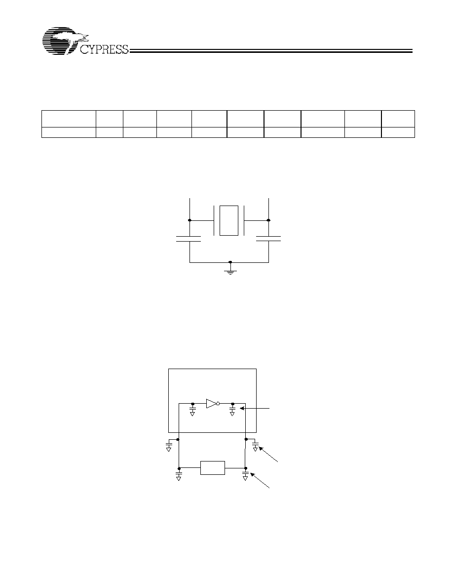
Crystal Loading
Crystal loading plays a critical role in achieving low ppm perfor-
mance. To realize low ppm performance, the total capacitance
the crystal will see must be considered to calculate the appro-
priate capacitive loading (CL).The following diagram shows a
typical crystal configuration using the two trim capacitors. An
important clarification for the following discussion is that the
trim capacitors are in series with the crystal not parallel. It's a
common misconception that load capacitors are in parallel
with the crystal and should be approximately equal to the load
capacitance of the crystal. This is not true.
Calculating Load Capacitors
In addition to the standard external trim capacitors, trace
capacitance and pin capacitance must also be considered to
correctly calculate crystal loading. As mentioned previously,
the capacitance on each side of the crystal is in series with the
crystal.
This means the total capacitance on each side of the crystal
must be twice the specified crystal load capacitance (CL).
While the capacitance on each side of the crystal is in series
with the crystal, trim capacitors (Ce1,Ce2) should be calcu-
lated to provide equal capacitive loading on both sides.
As mentioned previously, the capacitance on each side of the
crystal is in series with the crystal. This mean the total capac-
itance on each side of the crystal must be 2 times the specified
load capacitance (CL).
While the capacitance on each side of the crystal is in series
with the crystal, trim capacitors(Ce1,Ce2) should be calcu-
lated to provide equal capacitative loading on both sides.
Table 7. Crystal Recommendations
Frequency
(Fund)
Cut
Loading Load Cap
Drive
(max.)
Shunt Cap
(max.)
Motional
(max.)
Tolerance
(max.)
Stability
(max.)
Aging
(max.)
14.31818 MHz
AT
Parallel
20 pF
0.1 mW
5 pF
0.016 pF
50 ppm
50 ppm
5 ppm
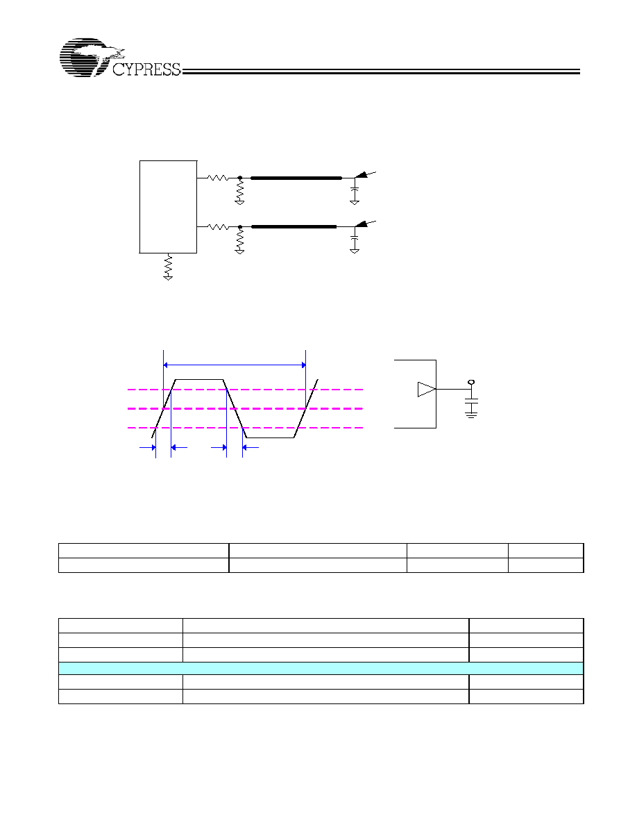
Figure 1. Crystal Capacitive Clarification
XTAL
Ce2
Ce1
Cs1
Cs2
X1
X2
Ci1
Ci2
Clock Chip
(CY28326)
Trace
2.8pF
Trim
33pF
Pin
3 to 6p
Figure 2. Crystal Loading Example
CY28326
Document #: 38-07616 Rev. *A
Page 11 of 23
Use the following formulas to calculate the trim capacitor
values fro Ce1 and Ce2.
CL .................................................. Crystal load capacitance
CLe ................................................ Actual loading seen by
crystal using standard value trim capacitors
Ce .................................................. External trim capacitors
Cs........................................... CStray capacitance (trace,etc)
Ci ............. Internal capacitance (lead frame, bond wires etc)
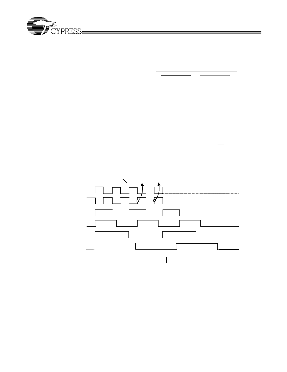
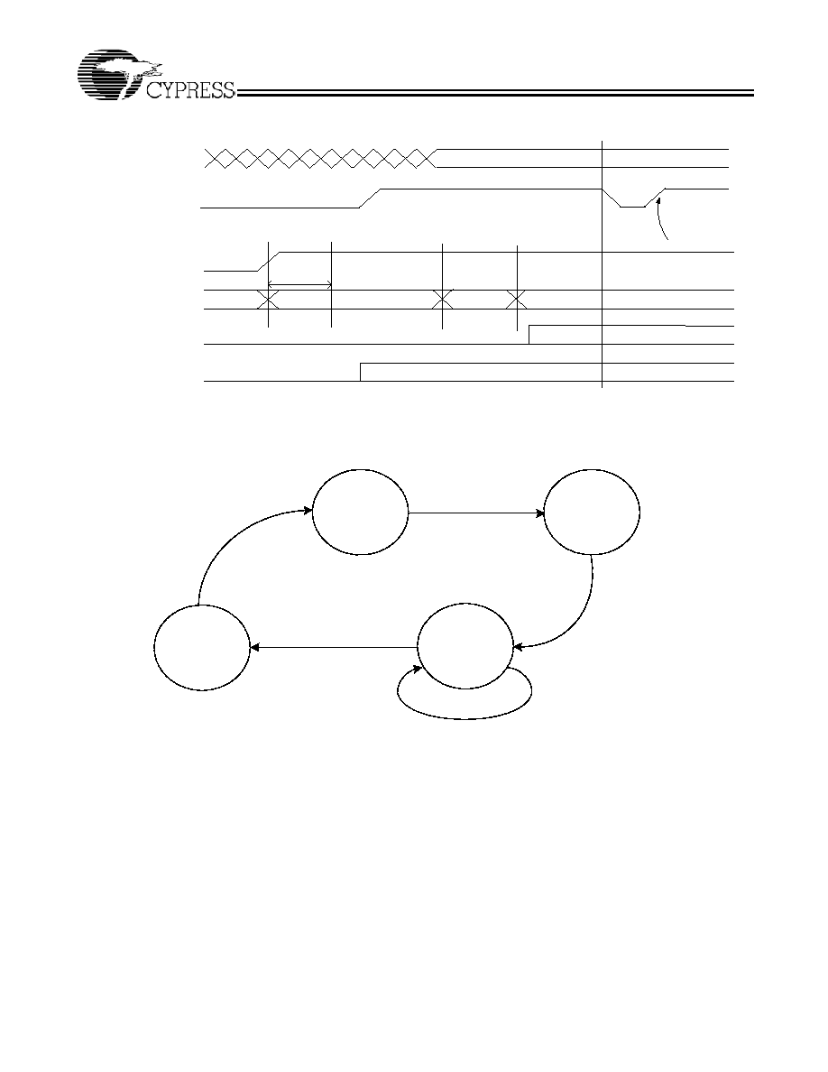
PD# (Power-down) Clarification
The PD# (Power Down) pin is used to shut off ALL clocks prior
to shutting off power to the device. PD# is an asynchronous
active LOW input. This signal is synchronized internally to the
device powering down the clock synthesizer. PD# is an
asynchronous function. When PD# is low, all clocks are driven
to a LOW value and held there and the VCO and PLLs are also
powered down. All clocks are shut down in a synchronous
manner so as not to cause glitches while transitioning to the
low `stopped' state.
PD# ≠ Assertion
When PD# is sampled low by two consecutive rising edges of
CPUC clock then all clock outputs (except CPU) clocks must
be held low on their next high to low transition. CPU clocks
must be driven high with a value of 2x Iref and CPUC undriven.
Due to the state of internal logic, stopping and holding the REF
clock outputs in the LOW state may require more than one
clock cycle to complete
Load Capacitance (each side)
Total Capacitance (as seen by the crystal)
Ce = 2 * CL - (Cs + Ci)
Ce1 + Cs1 + Ci1
1
+
Ce2 + Cs2 + Ci2
1
(
)
1
=
CLe
PD#
AGP, 66MHz
48MHz
PCI, 33MHz
REF, 14.31818
SRC, 25MHz
CPUC,
133MHz
CPUT, 133MHz
Figure 3. Power-down Assertion Timing Waveforms
CY28326
Document #: 38-07616 Rev. *A
Page 12 of 23
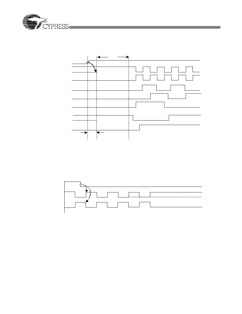
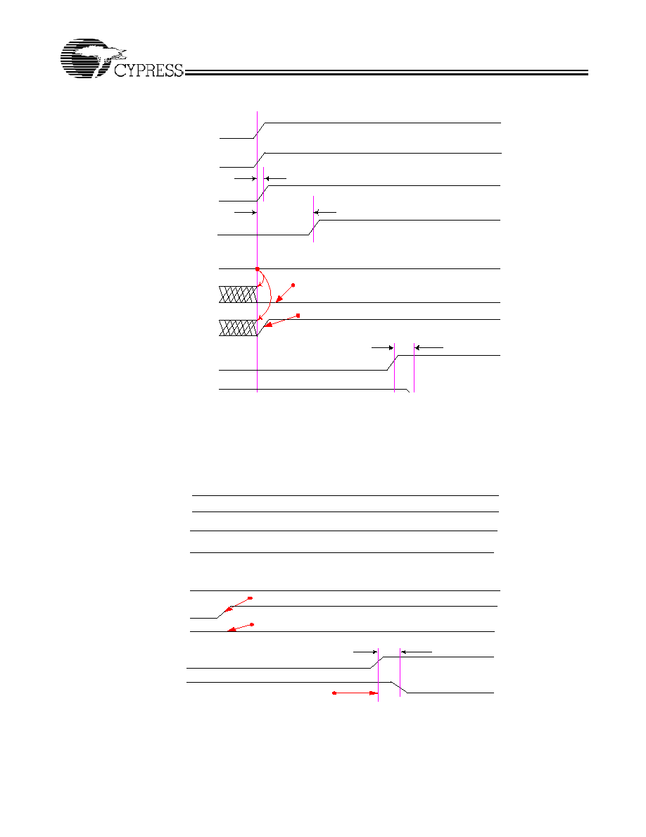
PD# De-assertion
The power-up latency between PD# rising to a valid logic `1'
level and the starting of all clocks is less than 3.0 ms.
CPU_STP# Assertion
The CPU_STP# signal is an active low input used for
synchronous stopping and starting the CPU output clocks
while the rest of the clock generator continues to function.
When the CPU_STP# pin is asserted, all CPU outputs that are
set with the SMBus configuration to be stoppable via assertion
of CPU_STP# will be stopped after being sampled by three
rising edges of the internal CPUT clock. The final states of the
stopped CPU signals are CPUT = HIGH and CPUC = LOW.
There is no change to the output drive current values during
the stopped state. The CPUT is driven HIGH with a current
value equal to (Mult 0 `select') x (Iref), and the CPUC signal
will not be driven. Due to the external pull-down circuitry,
CPUC will be LOW during this stopped state.
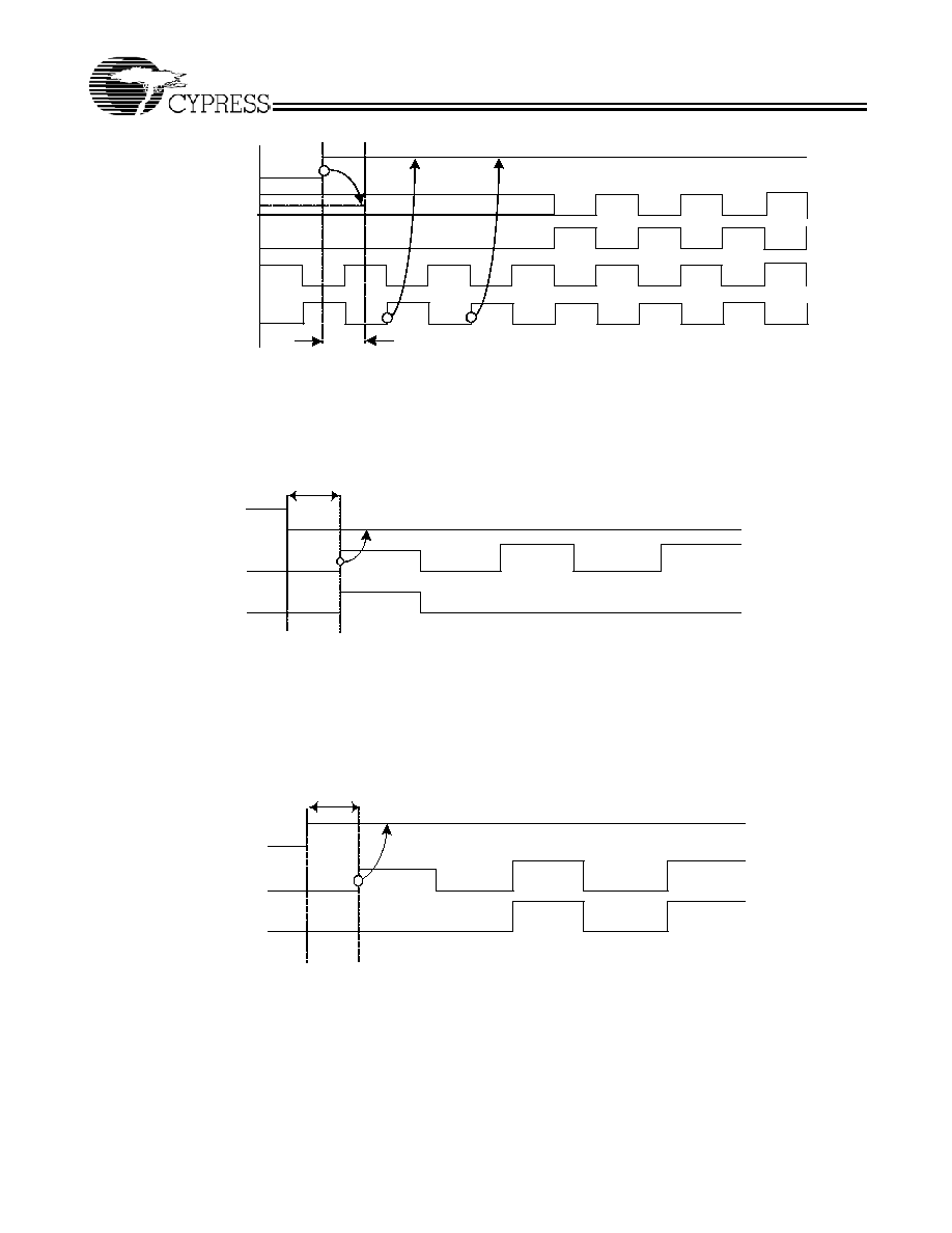
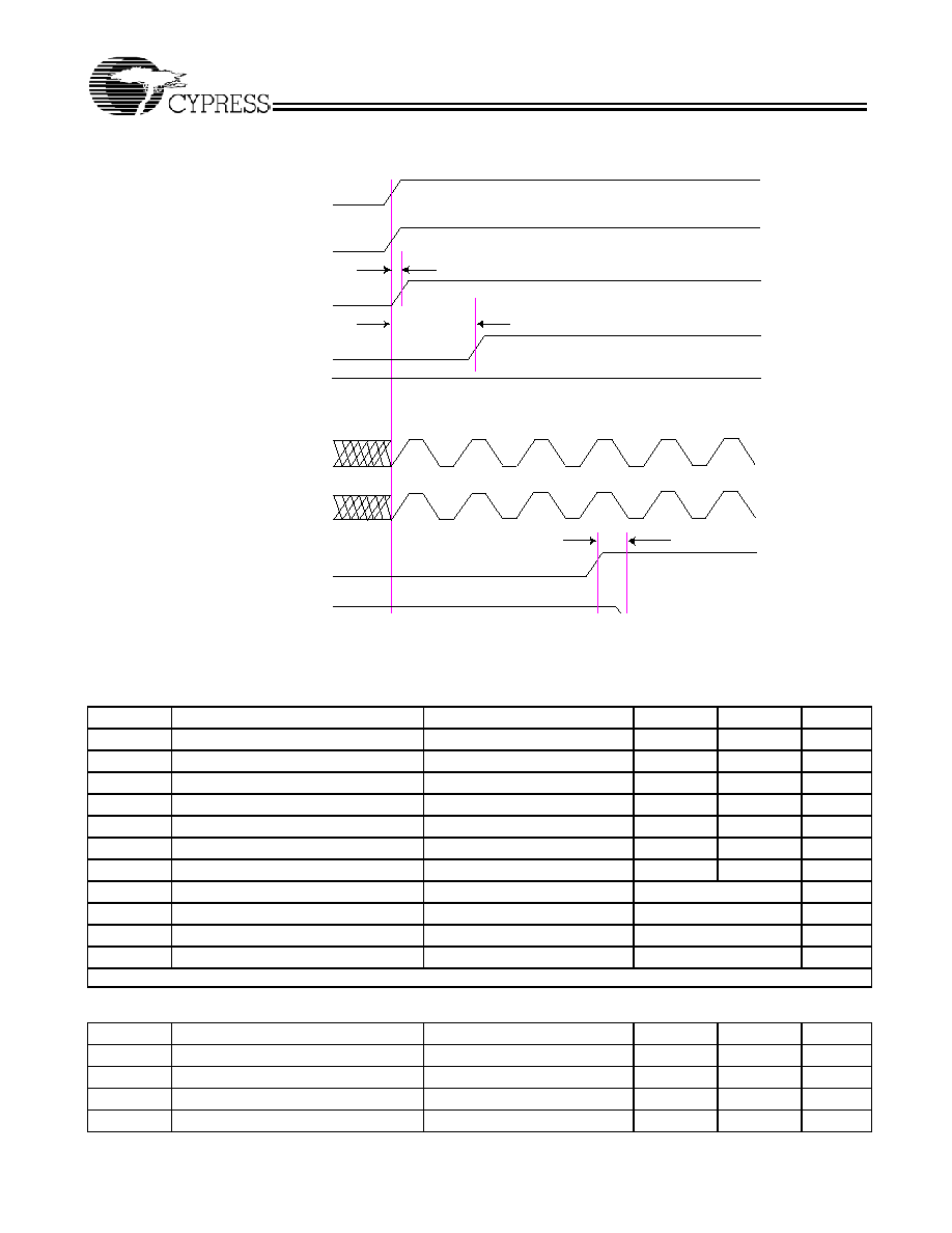
CPU_STP# De-assertion
The de-assertion of the CPU_STP# signal will cause all CPU
outputs that were stopped to resume normal operation in a
synchronous manner.
Synchronous manner meaning that no short or stretched clock
pulses will be produce when the clock resumes. The maximum
latency from the deassertion to active outputs is no more than
three CPU clock cycles.
REF, 14.31818
Tdrive_PD#
<300
µS, >200mV
PD#
CPUC,
133MHz
CPUT, 133MHz
AGP, 66MHz
48MHz
PCI, 33MHz
SRC, 25MHz
Tstable
<1.8ms
Figure 4. Power-down De-assertion Timing Waveforms
CPU_STP#
CPUT
CPUC
Figure 5. CPU_STP# Assertion Waveform
CY28326
Document #: 38-07616 Rev. *A
Page 13 of 23
PCI_STP# Assertion
[2]
The PCI_STP# signal is an active LOW input used for
synchronous stopping and starting the PCI outputs while the
rest of the clock generator continues to function.
The set-up time for capturing PCI_STP# going LOW is 10 ns
(t
SU
). (See Figure 7.)
PCI_STP# Deassertion
The deassertion of the PCI_STP# signal will cause all PCI
clocks to
resume running in a synchronous manner within two PCI clock
periods after PCI_STP# transitions to a high level.
Note:
2.
The PCI STOP function is controlled by PCI_STP# pin number 19.
CPU_STP#
CPUT
CPUC
CPU Internal
Tdrive_CPU_STP#,10nS>200mV
Figure 6. CPU_STP# De-assertion Waveform
Tsu
PCI_STP#
PCI_F
PCI
Figure 7. PCI_STP# Assertion Waveform
PCI_STP#
PCI_F
PCI
Tsu
Figure 8. PCI_STP# Deassertion Waveform
CY28326
Document #: 38-07616 Rev. *A
Page 14 of 23
F S[D:A]
VT T _PWRG D
PW RG D_VRM
VDD Clock Gen
Clock State
Clock Outputs
Clock VCO
0.2-0.3mS
Delay
State 0
State 2
State 3
Wait for
VT T _PWRG D
Sample Sels
Off
Off
On
On
State 1
Device is not affected,
VT T _PWRG D is ignored.
And this pin become PD#
function
Figure 9. VTT_PWRGD Timing Diagram
VTT_PWRGD = High
Delay
>0.25mS
S1
Power Off
S0
VDD_A = 2.0V
Sample
Inputs straps
S2
Normal
Operation
Wait for <1.8ms
Enable Outputs
S3
VTT_PWRGD = toggle
VDD_A = off
Figure 10. Clock Generator Power-up/Run State Diagram
CY28326
Document #: 38-07616 Rev. *A
Page 15 of 23
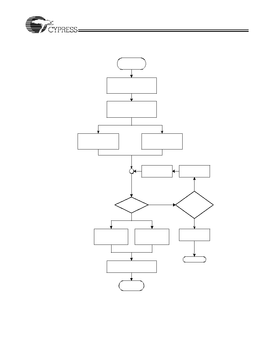
Figure 11. Watch Dog timer flowchart for BIOS programming
RESET WATCHDOG TIMER
Set WD Timer Bits = 0
Clear WD Alarm bit = 0
INITIALIZE WATCHDOG TIMER
Set Frequency Revert Bit
Set WD Timer Bits
CHANGE FREQ BY
SET SOFTWARE FSEL
Set SW Freq_Sel bits
Set FS override bit
CHANGE FREQ BY SET DIAL-A-
FREQUENCY
Load M and N Registers
Set Pro_Freq_EN = 1
NO
Reset & Revert
Frequency back
Frequency Revert Bit = 0
Set Frequency to
FS_HW_Latched
Frequency Revert Bit = 1
Set Frequency to
FS_SW Setting
SRESET# = 0 for 3 msec
WATCHDOG TIMER
PROGRAMMING
System need Extend
Time for next count
WD Alarm bit = 1
Exit WD Timer
CLEAR WD TIMER
Set WD timer Bits = 0
WD timer Reload bit
setting from 0 to 1
Set WD Timer Bits to
Extend Time
YES
NO
YES
CY28326
Document #: 38-07616 Rev. *A
Page 16 of 23
280us
VTT_PWRGD
POR(Power On
Reset)
Situation 1 : Power on & Ratio initial by HW strapping
VCC3
Lo
Ratio Select PIN
Lo
(PIN20)Ratio1/
PCI6
Hi
(PIN19)Ratio0/
PCI5
When Power up Ratio Select PIN = "Lo" then
PIN19,PIN20 become Ratio Function PIN
Power up PIN19 default = Ratio 0 follow HW FSA
Strapping
1ms
System Power
OK
PCI RESET
20us
Power up PIN20 default = Ratio 1 follow HW FSB
Strapping
MODE
Figure 12. Situation 1: Power on & Ratio initial by HW strapping
P o w e r s e q u e n c e f o r R a t io P IN
S it u a t io n 2 : B IO S p r o g r a m m in g S W F S E L t a b le a n d S y s t e m r e s e t
b y W a t c h d o g t im e r r e s e t fu n c t io n ( N O F r e q u e c n y r e c o v e r y ) .
V T T _ P W R G D
P O R ( P o w e r O n
R e s e t )
V C C 3
L o
R a t io S e le c t P IN
( P IN 2 0 ) R a t io 1 /
P C I6
H i
( P IN 1 9 ) R a t io 0 /
P C I5
1 m s
S y s t e m P o w e r
O K
P C I R E S E T
S y s t e m S t r a p p in g F r e q R a t io in t h is
p o in t
A f t e r B IO S p r o g r a m m in g S W F S E L R a t io 1 s w it c h t o n e w S W
F S 1 v a lu e
H i
H i
H i
H i
A f t e r B IO S p r o g r a m m in g S W F S E L R a t io 0 s w it c h t o n e w S W
F S 0 v a lu e
M O D E
H i
Figure 13. BIOS programming SW FSEL table and System reset by
Watch timer reset function (NO Frequency recovery).
CY28326
Document #: 38-07616 Rev. *A
Page 17 of 23
280us
VTT_PWRGD
Situation 3 : Power on & Ratio PIN switch to PCI clock
VCC3
1
Ratio Select PIN
When Power up Ratio Select PIN ="Hi" then
PIN19,PIN20 become PCI clock PIN
1ms
System Power
OK
PCI RESET
20us
POR(Power On
Reset)
(PIN20)Ratio1/
PCI6
(PIN19)Ratio0/
PCI5
MODE
Figure 14. Power on & Ratio PIN switch to PCI clock
Absolute Maximum Conditions
Parameter
Description
Condition
Min.
Max.
Unit
V
DD
Core Supply Voltage
≠0.5
4.6
V
V
DDA
Analog Supply Voltage
≠0.5
4.6
V
V
IN
Input Voltage
Relative to V
SS
≠0.5
V
DD
+ 0.5
VDC
T
S
Temperature, Storage
Non Functional
≠65
+150
∞C
T
A
Temperature, Operating Ambient
Functional
0
70
∞C
T
J
Temperature, Junction
Functional
≠
150
∞C
ESD
HBM
ESD Protection (Human Body Model)
MIL-STD-883, Method 3015
2000
≠
V
ÿ
JC
Dissipation, Junction to Case
Mil-Spec 883E Method 1012.1
36.92
∞C/W
ÿ
JA
Dissipation, Junction to Ambient
JEDEC (JESD 51)
83.52
∞C/W
UL≠94
Flammability Rating
At 1/8 in.
V≠0
MSL
Moisture Sensitivity Level
1
Multiple Supplies: The Voltage on any input or I/O pin cannot exceed the power pin during power-up. Power supply sequencing is NOT required.
DC Electrical Specifications
Parameter
Description
Condition
Min.
Max.
Unit
V
DD
, V
DDA
3.3 Operating Voltage
3.3V ± 5%
3.135
3.465
V
V
ILI2C
Input Low Voltage
SDATA, SCLK
≠
1.0
V
V
IHI2C
Input High Voltage
SDATA, SCLK
2.2
≠
V
V
IL
Input Low Voltage
V
SS
≠0.5
0.8
V
CY28326
Document #: 38-07616 Rev. *A
Page 18 of 23
V
IH
Input High Voltage
2.0
V
DD
+0. 5
V
I
IL
Input Leakage Current
except Pull-ups or Pull downs
0 < V
IN
< V
DD
≠5
5
µA
V
OL
Output Low Voltage
I
OL
= 1 mA
≠
0.4
V
V
OH
Output High Voltage
I
OH
= ≠1 mA
2.4
≠
V
I
OZ
High-Impedance Output Current
≠10
10
µA
C
IN
Input Pin Capacitance
2
5
pF
C
OUT
Output Pin Capacitance
3
6
pF
L
IN
Pin Inductance
≠
7
nH
V
XIH
Xin High Voltage
0.7V
DD
V
DD
V
V
XIL
Xin Low Voltage
0
0.3V
DD
V
I
DD
Dynamic Supply Current
At 200 MHz and all outputs
loaded per Table 8 and Figure 15
≠
350
mA
AC Electrical Specifications
Parameter
Description
Condition
Min.
Max.
Unit
Crystal
T
DC
XIN Duty Cycle
The device will operate
reliably with input duty cycles
up to 30/70 but the REF clock
duty cycle will not be within
specification
47.5
52.5
%
T
PERIOD
XIN period
When Xin is driven from an
external clock source
69.841
71.0
ns
T
R
/ T
F
XIN Rise and Fall Times
Measured between 0.3V
DD
and 0.7V
DD
≠
10.0
ns
T
CCJ
XIN Cycle to Cycle Jitter
As an average over 1
µs
duration
≠
500
ps
L
ACC
Long Term Accuracy
Over 150 ms
300
ppm
CPU at 0.7V
T
DC
CPUT and CPUC Duty Cycle
Measured at crossing point V
OX
38
62
%
T
PERIOD
100 MHz CPUT and CPUC Period
Measured at crossing point V
OX
9.9970
10.003
ns
T
PERIOD
133 MHz CPUT and CPUC Period
Measured at crossing point V
OX
7.4978
7.5023
ns
T
PERIOD
166 MHz CPUT and CPUC Period
Measured at crossing point V
OX
5.9982
6.0018
ns
T
PERIOD
200 MHz CPUT and CPUC Period
Measured at crossing point V
OX
4.9985
5.0015
ns
T
SKEW
Any CPUT/C to CPUT/C Clock Skew
Measured at crossing point V
OX
≠
±110
ps
T
CCJ
CPUT/C Cycle to Cycle Jitter
Measured at crossing point V
OX
≠
250
ps
T
R
/ T
F
CPUT and CPUC Rise and Fall Times
Measured from Vol = 0.175 to
Voh = 0.525V
175
1300
ps
T
R
Rise Time Variation
≠
550
ps
T
F
Fall Time Variation
≠
550
ps
V
HIGH
Voltage High
Math averages Figure 15
660
850
mv
V
LOW
Voltage Low
Math averages Figure 15
≠150
≠
mv
V
OX
Crossing Point Voltage at 0.7V Swing
200
550
mv
V
OVS
Maximum Overshoot Voltage
≠
V
HIGH
+ 0.3
V
V
UDS
Minimum Undershoot Voltage
≠0.3
≠
V
V
RB
Ring Back Voltage
See Figure 15. Measure SE
≠
0.2
V
AGP
DC Electrical Specifications
Parameter
Description
Condition
Min.
Max.
Unit
CY28326
Document #: 38-07616 Rev. *A
Page 19 of 23
T
DC
AGP Duty Cycle
Measurement at 1.5V
44
56
%
T
PERIOD
Spread Disabled AGP Period
Measurement at 1.5V
14.9955
15.0045
ns
T
PERIOD
Spread Enabled AGP Period
Measurement at 1.5V
14.9955
15.0799
ns
T
HIGH
AGP High Time
Measurement at 2.0V
4.5000
8.0
ns
T
LOW
AGP Low Time
Measurement at 0.8V
4.5000
8.0
ns
T
R
/ T
F
AGP Rise and Fall Times
Measured between 0.8V and
2.0V
0.5
2.0
ns
T
SKEW
Any AGP to Any AGP Clock Skew
Measurement at 1.5V
≠
±550
ps
T
CCJ
AGP Cycle to Cycle Jitter
Measurement at 1.5V
≠
500
ps
PCI/PCIF
T
DC
PCI Duty Cycle
Measurement at 1.5V
45
55
%
T
PERIOD
Spread Disabled PCIF/PCI Period
Measurement at 1.5V
29.9910
30.0009
ns
T
PERIOD
Spread Enabled PCIF/PCI Period
Measurement at 1.5V
29.9910
30.1598
ns
T
HIGH
PCIF and PCI High Time
Measurement at 2.0V
11.0
15.0
ns
T
LOW
PCIF and PCI Low Time
Measurement at 0.8V
11.0
15.0
ns
T
R
/ T
F
PCIF and PCI Rise and Fall Times
Measured between 0.8V and
2.0V
0.5
2.0
ns
T
SKEW
Any PCI clock to Any PCI Clock Skew Measurement at 1.5V
≠
±700
ps
T
CCJ
PCIF and PCI Cycle to Cycle Jitter
Measurement at 1.5V
≠
550
ps
48M
T
DC
Duty Cycle
Measurement at 1.5V
45
55
%
T
PERIOD
Period Measurement
at 1.5V
20.8271
20.8396
ns
T
HIGH
48 MHz High Time
Measurement at 2.0V
8.000
10.386
ns
T
LOW
48 MHz Low Time
Measurement at 0.8V
8.000
10.386
ns
T
R
/ T
F
Rise and Fall Times
Measured between 0.8V and
2.0V
0.5
1.6
ns
T
CCJ
Cycle to Cycle Jitter
Measurement at 1.5V
≠
800
ps
T
SKEW
Any 48 MHz to 48 MHz clock skew
Measurement @1.5V
≠
±100
ps
25M
T
DC
Duty Cycle
Measurement at 1.5V
45
55
%
T
PERIOD
Period Measurement
at 1.5V
39.998
40.002
ns
T
HIGH
25 MHz High Time
Measurement at 1.5V
17.9999
20.000
ns
T
LOW
25 MHz Low Time
Measurement at 1.5V
17.9999
20.000
ns
T
R
/ T
F
Rise and Fall Times
Measured between 0.8V and
2.0V
0.4
2.0
ns
T
CCJ
Cycle to Cycle Jitter
Measurement at 1.5V
≠
350
ps
T
SKEW
Any 25 MHz to 25 MHz Clock Skew
Measurement @1.5V
≠
±100
ps
L
ACC
25MHz Long Term Accuracy
Measurement @1.5V
≠
50
ppm
REF
T
DC
REF Duty Cycle
Measurement at 1.5V
45
55
%
T
PERIOD
REF Period
Measurement at 1.5V
69.827
69.855
ns
T
R
/ T
F
REF Rise and Fall Times
Measured between 0.8V and
2.0V
0.45
1.8
ns
T
CCJ
REF Cycle to Cycle Jitter
Measurement at 1.5V
≠
1600
ps
T
SKEW
Any REF to REF clock skew
Measurement @1.5V
≠
500
ps
AC Electrical Specifications
(continued)
Parameter
Description
Condition
Min.
Max.
Unit
CY28326
Document #: 38-07616 Rev. *A
Page 20 of 23
ENABLE/DISABLE and SET-UP
T
STABLE
Clock Stabilization from Power-up
≠
1.8
ms
T
SS
Stopclock Set-up Time
10.0
≠
ns
T
SH
Stopclock Hold Time
0
≠
ns
Special Skew & Jitter Specification Requirement
CPU to CPU pin
to pin Skew
CPU group skew
Measured at crossing point V
OX
-100
100
ps
AGP to PCI pin to
pin Skew
AGP group to PCI group skew
AGP must leading PCI
Measurement at 1.5V
1
3
ns
Table 8. Maximum Lumped Capacitive Output Loads
Clock
Max Load
Unit
PCI Clocks
30
pF
AGP Clocks
30
pF
48M Clock
30
pF
25M Clock
30
pF
REF Clock
30
pF
AC Electrical Specifications
(continued)
Parameter
Description
Condition
Min.
Max.
Unit
CY28326
Document #: 38-07616 Rev. *A
Page 21 of 23
Test and Measurement Set-up
For Differential CPU and SRC Output Signals
The following diagram shows lumped test load configurations
for the differential Host Clock Outputs.
C P U T
T
P C B
T
P C B
C P U C
3 3
3 3
4 9 .9
4 9 .9
M e a s u re m e n t
P o in t
2 p F
4 7 5
IR E F
M e a s u re m e n t
P o in t
2 p F
Figure 15. 0.7V Load Configuration
Table 9. CPU Clock Current Select Function
Board Target Trace/Term Z
Reference R, I
REF
≠ V
DD
(3*R
REF
)
Output Current
V
OH
@ Z
50 Ohms
R
REF
= 475 1%, I
REF
= 2.32mA
I
OH
= 6*I
REF
0.7V @ 50
Figure 16. Lumped Load For Single-ended Output Signals (for AC Parameters Measurement)
0 V
3 .3 V
2 .4 V
0 .4 V
1 .5 V
tD C
T f
T r
O u tp u t u n d e r T e st
P ro b e
L o a s
C a p
Ordering Information
Part Number
Package Type
Product Flow
CY28326OC
48-pin SSOP
Commercial, 0
∞ to 70∞C
CY28326OCT
48-pin SSOP ≠ Tape and Reel
Commercial, 0
∞ to 70∞C
Lead Free (Planned)
CY28326OXC
48-pin SSOP
Commercial, 0
∞ to 70∞C
CY28326OXCT
48-pin SSOP ≠ Tape and Reel
Commercial, 0
∞ to 70∞C
CY28326
Document #: 38-07616 Rev. *A
Page 22 of 23
© Cypress Semiconductor Corporation, 2004. The information contained herein is subject to change without notice. Cypress Semiconductor Corporation assumes no responsibility for the use
of any circuitry other than circuitry embodied in a Cypress Semiconductor product. Nor does it convey or imply any license under patent or other rights. Cypress Semiconductor does not authorize
its products for use as critical components in life-support systems where a malfunction or failure may reasonably be expected to result in significant injury to the user. The inclusion of Cypress
Semiconductor products in life-support systems application implies that the manufacturer assumes all risk of such use and in doing so indemnifies Cypress Semiconductor against all charges.
Cypress products are not warranted nor intended to be used for medical, life-support, life-saving, critical control or safety applications, unless pursuant to an express written agreement with Cypress.
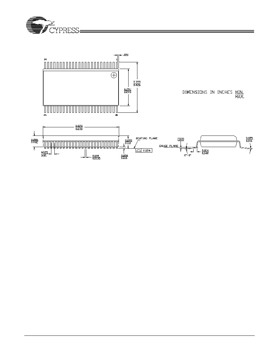
Package Drawing and Dimensions
Dial-A-Frequency is a registered trademark of Cypress Semiconductor Corporation. Dial-A-Ratio is a trademark of Cypress
Semiconductor Corporation.
Intel and Pentium are registered trademarks of Intel Corporation. All product and company names mentioned in this document
are the trademarks of their respective holders.
48-lead Shrunk Small Outline Package O48
51-85061-*C

CY28326
Document #: 38-07616 Rev. *A
Page 23 of 23
Document History Page
Document Title: CY28326 FTG for VIA PT880 Serial Chipset
Document #: 38-07616 Rev. *A
REV.
ECN NO. Issue Date
Orig. of
Change
Description of Change
**
224103
See ECN
RGL
New Data Sheet
*A
237729
See ECN
RGL
Updated the AC Electrical Specs based on the characterization result