 | –≠–ª–µ–∫—Ç—Ä–æ–Ω–Ω—ã–π –∫–æ–º–ø–æ–Ω–µ–Ω—Ç: CY28331OC | –°–∫–∞—á–∞—Ç—å:  PDF PDF  ZIP ZIP |
Clock Generator for AMDTM Hammer
CY28331
Cypress Semiconductor Corporation
∑
3901 North First Street
∑
San Jose
,
CA 95134
∑
408-943-2600
Document #: 38-07491 Rev. *B
Revised April 17, 2003
Features
∑ Supports AMD
Hammer CPU
∑ Two differential pairs of CPU clocks
∑ Eight low-skew/low-jitter PCI clocks
∑ One free-running PCI clock
∑ Four low-skew/low-jitter PCI/HyperTransport
clocks
∑ One 48M output for USB
∑ One programmable 24M or 48M for FDC
∑ Three REF 14.318-MHz clocks
∑ Dial-a-Frequency
programmability
∑ Lexmark Spread Spectrum for optimal electromagnetic
interference (EMI) reduction
∑ SMBus register-programmable options
∑ 5V-tolerance SCLK and SDATA lines
∑ 3.3V operation
∑ Power management control pins
∑ 48-pin SSOP package
Note:
1.
HCLK, 66 MHz, and 33 MHz are in phase and synchronous at power-up.
Table 1. Frequency Table (MHz)
[1]
FS
(3:0)
PCI_HT
SEL
CPU
HT66
PCI
0000
X
High-Z
(All outputs except XOUT are three-stated)
0001
0/1
133.9
67.0/33.5
33.5
0010
0/1
166.9
66.8/33.4
33.4
0011
0/1
200.9
67.0/33.5
33.5
0100
0/1
100.0
66.7/33.3
33.3
0101
0/1
133.3
66.7/33.3
33.3
0110
0/1
166.7
66.7/33.3
33.3
0111
(default)
0/1
200.0
66.7/33.3
33.3
1000
0/1
105.0
70.0/35.0
35.0
1001
0/1
110.0
73.3/36.7
36.7
1010
0/1
210.0
70.0/35.0
35.0
1011
0/1
240.0
60.0/30.0
30.0
1100
0/1
270.0
67.5/33.8
33.8
1101
0/1
233.3
58.3/29.2
29.2
1110
0/1
266.7
66.7/33.3
33.3
1111
0/1
300.0
75.0/37.5
37.5
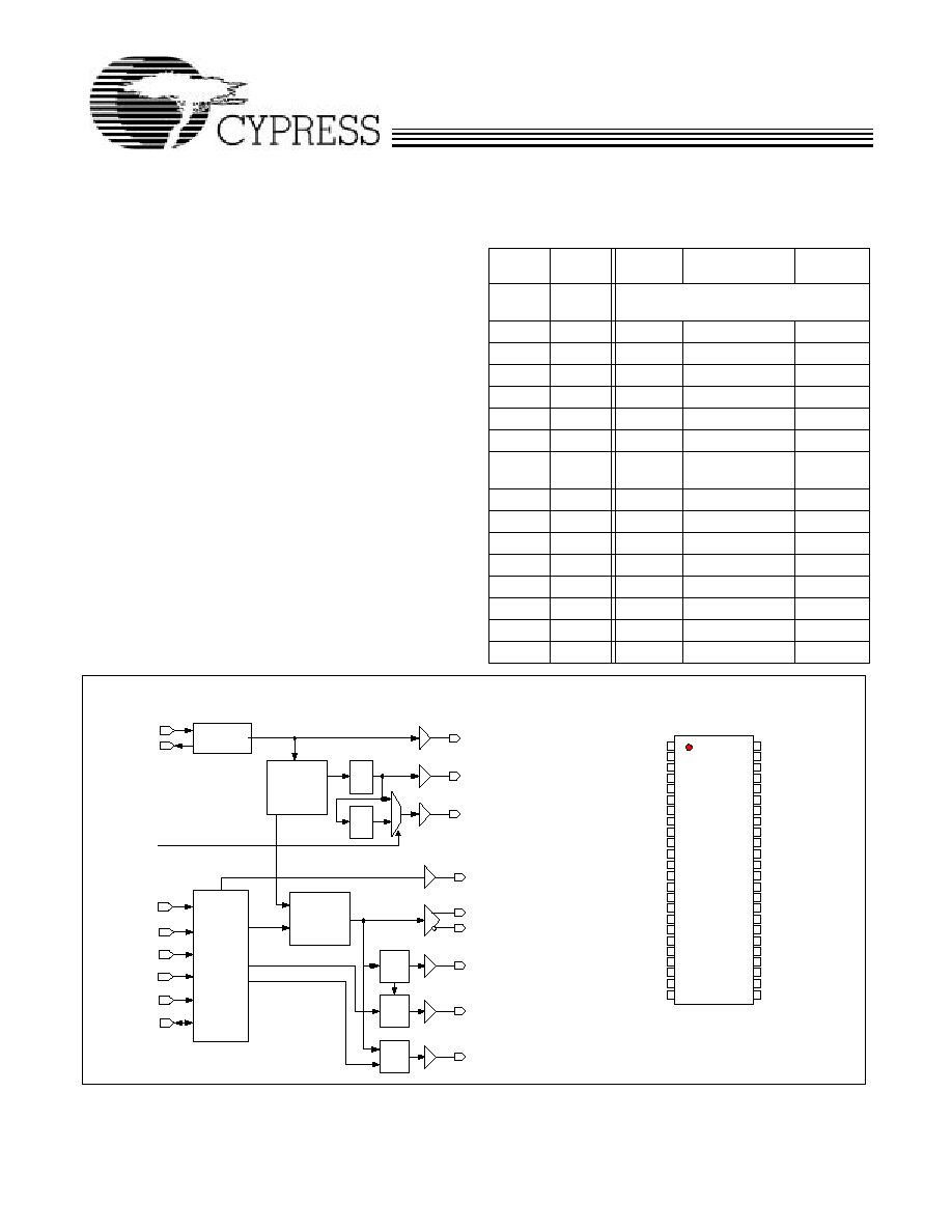
Block Diagram
Pin Configuration
XIN
XOUT
REF(0:2)
USB
24_48MHz
CPUT(0:1)
CPUC(0:1)
PCI33_F
PCI33_(0:7)
PCI33_HT66_(0:3)
SEL#
FS(0:3)
PCISTOP#
SPREAD
SCLK
14.31818MHz
XTAL
PLL1
/4
/2
PLL2
/N
STOP
CNTL
Control
Logic
SDATA
PD#
SRESET#
1
2
3
4
5
6
7
8
9
10
11
12
13
14
15
16
17
18
19
20
21
22
23
24
48
47
46
45
44
43
42
41
40
39
38
37
36
35
34
33
32
31
30
29
28
27
26
25
*FS0/REF0
VDD
XIN
XOUT
VSS
PCI33HT66_0/*PCI33HT66SEL0#
PCI33HT66_1/*PCI33HT66SEL1#
PCI33_HT66_2
VDD
VSS
PCI33_HT66_3
PCI33_7
PCI33_0
PCI33_1
VSS
VDD
PCI33_2
PCI33_3
VDD
VSS
PCI33_4
PCI33_5
PCISel/PCI33_F
*PCI33_6/PCISTOP#
**FS1/REF1
VSS
VDD
*FS2/REF2
SRESET#/PD#
VDDA
VSSA
CPUT0
CPUC0
VSS
VDD
CPUT1
CPUC1
VDD
VSS
VSSF
VDDF
**USB/FS3
VSS
VDD
24_48MHz/**SEL#
VSS
SDATA
SCLK
*100K Internal Pull-up
**100K Internal Pull-down
C
Y
2
833
1
CY28331
Document #: 38-07491 Rev. *B
Page 2 of 17
Pin Description
Pin
Name
PWR
I/O
Description
3
XIN
V
DD
I
Oscillator Buffer Input. Connect to a crystal or to an external clock.
4
XOUT
V
DD
O
Oscillator Buffer Output. Connect to a crystal. Do not connect when an
external clock is applied at XIN.
41, 37
CPUT(0:1)
V
DDC
O
CPU clock outputs 0 and 1: push-pull "true" output of differential pair.
40, 36
CPUC(0:1)
V
DDC
O
CPU clock outputs 0 and 1: push-pull "compliment" output of differential
pair.
13, 14, 17,
18, 21, 22
PCI33(0:5)
O
3.3V PCI clock outputs controlled by PCISTOP#.
23
PCISel /
PCI33_F
I/O
PCISel is a strap option during power-up to select Pin 24 functionality:
0: Configure Pin 24 as PCI33_6
1: Configure Pin 24 as PCISTOP# (default 100k internal pull-up)
After power-up, this pin reverts to standard PCI33_F output.
8, 11
PCI33_HT66(2:3)
V
DDD
O
3.3V PCI 33-MHz or HyperTransport
66 clock outputs. This group is
selectable between 33 MHz and 66 MHz, based on the state of
PCI33HT66SEL[0:1]#.
6, 7
PCI33_HT66_[0:1]/
PCI33_HT66SEL[0:1]#
V
DDD
I/O
PCI33 or HT66 select. This input strap selects the output frequency of
PCI33_HT66 outputs to either 33MHz or 66MHz. There is an internal
100Kohm pull-up resistor. After power-up, this pin becomes
PCI33_HT66_[0:1] output.
SEL1 SEL0
PIN6
PIN7
PIN8
PIN11
0
0
HT66_0
HT66_1
HT66_2
HT66_3
0
1
HT66_0
HT66_1
HT66_2
PCI33_3
1
0
HT66_0
HT66_1
PCI33_2 PCI33_3
1
1
HT66_0
PCI33_1
PCI33_2 PCI33_3
31
USB/FS3
I/O
3.3V USB clock output at 48 MHz. At power-up this pin is sensed to
determine the CPU output frequency. There is an internal 100K ohm
pull-down resistor.
28
24_48MHz/SEL#
I/O
3.3V super I/O clock output. At power-up this pin is sensed to determine
whether the output is 24 MHz or 48 MHz. There is an internal 100K ohm
pull-down resistor. This pin will be externally strapped high using a 10K
ohm resistor to V
SS
. 0 = 48 MHz, 1 = 24 MHz.
1, 48, 45
REF(0:2)/FS(0:2)
I/O
3.3V reference clock output. At power-up this pin is sensed to determine
the CPU output frequency. There is an internal 100K ohm pull-up resistor
for FS0, while FS(1:2) includes 100K ohm pull-up resistors.
44
SRESET#/PD#
I/O
Watchdog Time-out Reset Output. Power-down input (100Kinternal
pull-up).
24
PCI33_6/
PCISTOP#
I/O
When configured through pin 23 as PCI_STOP#, this pin controls the
PCI33(0:5,7) and PCI33_HT66(1:3) outputs. Active LOW control input to
halt all 33-MHz PCI clocks except PCI33_F. Only the PCI33_HT66 outputs
that are running at 33 MHz will be stopped. The outputs will be glitch-free
when turning off and turning on (100K internal pull-up). When configured
through pin 23 as PCI33_6, PCI_STOP# is unavailable.
12
PCI33_7
O
3.3V PCI clock outputs controlled by PCISTOP#.
26
SDATA
I/O
Data pin for SMBus (rev2.0). There is an internal 100K ohm pull-up
resistor.
25
SCLK
I
Clock pin for SMBus (rev2.0). There is an internal 100K ohm pull-up
resistor.
2, 9, 16,
19, 29, 35,
38, 46
V
DD
PWR Power connection to 3.3V for the core.
5, 10, 15,
20, 27, 30,
34, 39, 47
V
SS
GND Power connection to GROUND for the CORE section of the chip.
43
V
DDA
PWR Power connection to 3.3V for the ANALOG section of the chip.

CY28331
Document #: 38-07491 Rev. *B
Page 3 of 17
Serial Data Interface
To enhance the flexibility and function of the clock synthesizer,
a two-signal serial interface is provided. Through the Serial
Data Interface (SDI), various device functions, such as
individual clock output buffers, can be individually enabled or
disabled. The registers associated with the SDI initializes to
their default setting upon power-up, and therefore use of this
interface is optional. Clock device register changes are
normally made upon system initialization, if any are required.
The interface can also be used during system operation for
power management functions.
Data Protocol
The clock driver serial protocol accepts byte write, byte read,
block write, and block read operations from the controller. For
block write/read operation, the bytes must be accessed in
sequential order from lowest to highest byte (most significant
bit first) with the ability to stop after any complete byte has
been transferred. For byte write and byte read operations, the
system controller can access individually indexed bytes. The
offset of the indexed byte is encoded in the command code,
as described in Table 2.
The block write and block read protocol is outlined in Table 3
while Table 4 outlines the corresponding byte write and byte
read protocol. The slave receiver address is 11010010 (D2h).
42
V
SSA
GND Power connection to GROUND for the analog section of the chip.
32
V
DDF
PWR Power connection to 3.3V for the 48-MHz PLL section of the chip.
33
V
SSF
GND Power connection to GROUND for the 48-MHz PLL section of the chip.
Pin Description
(continued)
Pin
Name
PWR
I/O
Description
Table 2. Command Code Definition
Bit
Description
7
0 = Block read or block write operation, 1 = Byte read or byte write operation.
(6:0)
Byte offset for byte read or byte write operation. For block read or block write operations, these bits
should be '0000000.'
Table 3. Block Read and Block Write Protocol
Block Write Protocol
Block Read Protocol
Bit
Description
Bit
Description
1
Start
1
Start
2:8
Slave address ≠ 7 bits
2:8
Slave address ≠ 7 bits
9
Write = 0
9
Write = 0
10
Acknowledge from slave
10
Acknowledge from slave
11:18
Command Code ≠ 8 bits
'00000000' stands for block operation
11:18
Command Code ≠ 8 bits
'00000000' stands for block operation
19
Acknowledge from slave
19
Acknowledge from slave
20:27
Byte Count ≠ 8 bits
20
Repeat start
28
Acknowledge from slave
21:27
Slave address ≠ 7 bits
29:36
Data byte 1 ≠ 8 bits
28
Read = 1
37
Acknowledge from slave
29
Acknowledge from slave
38:45
Data byte 2 ≠ 8 bits
30:37
Byte count from slave ≠ 8 bits
46
Acknowledge from slave
38
Acknowledge
....
......................
39:46
Data byte from slave ≠ 8 bits
....
Data Byte (N≠1) ≠ 8 bits
47
Acknowledge
....
Acknowledge from slave
48:55
Data byte from slave ≠ 8 bits
....
Data Byte N ≠ 8 bits
56
Acknowledge
....
Acknowledge from slave
....
Data bytes from slave/Acknowledge
....
Stop
....
Data byte N from slave ≠ 8 bits
....
Not Acknowledge
....
Stop

CY28331
Document #: 38-07491 Rev. *B
Page 4 of 17
Serial Control Registers
Table 4. Byte Read and Byte Write Protocol
Byte Write Protocol
Byte Read Protocol
Bit
Description
Bit
Description
1
Start
1
Start
2:8
Slave address ≠ 7 bits
2:8
Slave address ≠ 7 bits
9
Write = 0
9
Write = 0
10
Acknowledge from slave
10
Acknowledge from slave
11:18
Command Code ≠ 8 bits
'1xxxxxxx' stands for byte operation, bits[6:0] of the
command code represents the offset of the byte to be
accessed
11:18
Command Code ≠ 8 bits
'1xxxxxxx' stands for byte operation, bits[6:0] of the
command code represents the offset of the byte to
be accessed
19
Acknowledge from slave
19
Acknowledge from slave
20:27
Data byte from master ≠ 8 bits
20
Repeat start
28
Acknowledge from slave
21:27
Slave address ≠ 7 bits
29
Stop
28
Read = 1
29
Acknowledge from slave
30:37
Data byte from slave ≠ 8 bits
38
Not Acknowledge
39
Stop
Byte 0: Frequency and Spread Spectrum Control Register
Bit
@Pup
Pin#
Name
Description
7
Inactive = 0
Write Disable (write once). A 1 written to this bit after a 1 has been written to Byte0
bit0 will permanently disable modification of all configuration registers until the part
has been powered off. Once the clock generator has been Write Disabled, the
SMBus controller should still accept and acknowledge subsequent write cycles but
it should not modify any of the registers.
6
0
For Test, always program to `0'
5
1
12
PCI33_7
enable (1 = Enabled, 0 = Disabled)
4
FS3 pin
31
FS3
corresponds to Frequency Selection. See Table 1.
3
FS2 pin
45
FS2
corresponds to Frequency Selection. See Table 1.
2
FS1 pin
48
FS1
corresponds to Frequency Selection. See Table 1.
1
FS0 pin
1
FS0
corresponds to Frequency Selection. See Table 1.
0
Inactive = 0
Write Enable. A 1 written to this bit after power-up will enable modification of all
configuration registers and subsequent 0's written to this bit will disable modification
of all configuration except this single bit. Note that block write transactions to the
interface will complete, however unless the interface has been previously unlocked,
the writes will have no effect. The effect of writing this bit doe not take effect until
the subsequent block write command.
Byte 1: PCI Clock Control Register
Bit
@Pup
Pin#
Name
Description
7
1
23
PCI33_F
enable (1 = Enabled, 0 = Disabled)
6
1
24
PCI33_6
enable (1 = Enabled, 0 = Disabled)
5
1
22
PCI33_5
enable (1 = Enabled, 0 = Disabled)
4
1
21
PCI33_4
enable (1 = Enabled, 0 = Disabled)
3
1
18
PCI33_3
enable (1 = Enabled, 0 = Disabled)
2
1
17
PCI33_2
enable (1 = Enabled, 0 = Disabled)
1
1
14
PCI33_1
enable (1 = Enabled, 0 = Disabled)
0
1
13
PCI33_0
enable (1 = Enabled, 0 = Disabled)
CY28331
Document #: 38-07491 Rev. *B
Page 5 of 17
Byte 2: USB, 24≠48MHz, REF(0:2) Control Register
Bit
@Pup
Pin #
Name
Description
7
active = 1
37, 36
CPUT/C(1) CPUT/C(1) shutdown. This bit can be optionally used to disable the CPUT/C(1)
clock pair. During shutdown, CPUT = low and CPUC = high
6
active = 1
41, 40
CPUT/C(0) CPUT/C(0) shutdown. This bit can be optionally used to disable the CPUT/C(0)
clock pair. During shutdown, CPUT = low and CPUC = high
5
active = 1
45
REF2
enable (1 = Enabled, 0 = Disabled)
4
active = 1
48
REF1
enable (1 = Enabled, 0 = Disabled)
3
active = 1
1
REF0
enable (1 = Enabled, 0 = Disabled)
2
active = 1
28
24_48MHz enable (1 = Enabled, 0 = Disabled)
1
active = 1
31
USB
enable (1 = Enabled, 0 = Disabled)
0
0
For Test, always program to `0'
Byte 3: PCI Clock Free Running Select Control Register
Bit
@Pup
Pin #
Name
Description
7
Inactive = 0
PCI_DRV
0 = Low Strength
1 = High Strength
6
Inactive = 0
PCI33_HT66 Drive Strength
0 = Low Strength
1 = High Strength
5
Inactive = 0
22
PCI5
free running enable (10 = Free running, 0 = Disabled)
4
Inactive = 0
21
PCI4
free running enable (1 = Free running, 0 = Disabled)
3
Inactive = 0
18
PCI3
free running enable (1 = Free running, 0 = Disabled)
2
1
11
PCI33_HT66_3 enable (1 = Enabled, 0 = Disabled)
1
1
8
PCI33_HT66_2 enable (1 = Enabled, 0 = Disabled)
0
1
7
PCI33_HT66_1 enable (1 = Enabled, 0 = Disabled)
Byte 4: Pin Latched/Real-time State
Bit
@Pup
Pin#
Name
Description
7
1
6
PCI33_HT66_0
enable (1 = Enabled, 0 = Disabled)
6
HW
24_48MHz/SEL#
pin power-up latched state
5
0
Reserved
For Test, always program to `0'
4
1
SSEN
Spread Spectrum enable (0 = disable, 1 = enable).
This bit provides a SW programmable control for spread spectrum clocking.
3
FS3 pin
31
FS3
power-up latched state
2
FS2 pin
45
FS2
power-up latched state
1
FS1 pin
48
FS1
power-up latched state
0
FS0 pin
1
FS0
power-up latched state
Byte 5: SSCG, Dial-a-SkewTM, and Dial-a-RatioTM Register
Bit
@Pup
Description
7
0
Spread Spectrum Selection:
bit7
bit6
bit5
% Spread
0
0
0
≠1.5
0
0
1
≠1.0
0
1
0
≠0.7
0
1
1
≠0.5 (default)
1
0
0
±0.75
1
0
1
±0.50
1
1
0
±0.35
1
1
1
±0.25
6
1
5
1