 | –≠–ª–µ–∫—Ç—Ä–æ–Ω–Ω—ã–π –∫–æ–º–ø–æ–Ω–µ–Ω—Ç: CY28341-2 | –°–∫–∞—á–∞—Ç—å:  PDF PDF  ZIP ZIP |
Universal Clock Chip for VIATMP4M/KT/KM400
DDR Systems
CY28341-2
Cypress Semiconductor Corporation
∑
3901 North First Street
∑
San Jose
,
CA 95134
∑
408-943-2600
Document #: 38-07471 Rev. *B
Revised April 22, 2003
Features
∑ Supports VIA
P4M/KM/KT/266/333/400 chipsets
∑ Supports Pentium
Æ
4, AthlonTM processors
∑ Supports two DDR DIMMS
∑ Supports three SDRAM DIMMS at 100 MHz
∑ Provides:
-- two different programmable CPU clock pairs
-- six differential SDRAM DDR pairs
-- three low-skew/-jitter AGP clocks
-- seven low-skew/-jitter PCI clocks
-- one 48M output for USB
-- one programmable 24M or 48M for SIO
∑ Dial-a-Frequency
and Dial-a-dB
features
∑ Spread Spectrum for best electromagnetic interference
(EMI) reduction
∑ Watchdog feature for system recovery
∑ SMBus-compatible for programmability
∑ 56-pin SSOP and TSSOP packages
Note:
1.
Pins marked with [*] have internal pull-up resistors. Pins marked with [**] have internal pull-down resistors.
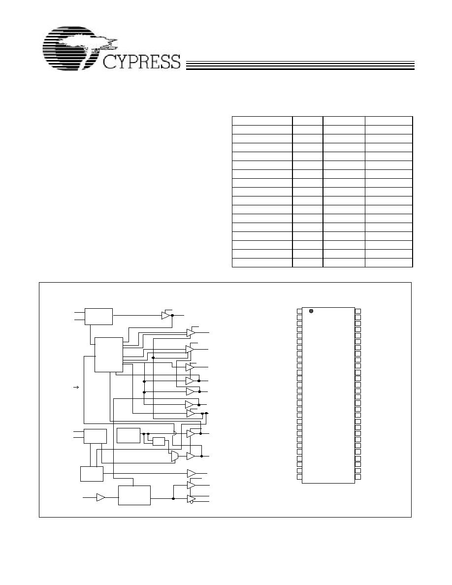
Table 1. Frequency Selection Table
FS(3:0)
CPU
AGP
PCI
0000
66.80
66.80
33.40
0001
100.00
66.80
33.40
0010
120.00
60.00
30.00
0011
133.33
66.67
33.33
0100
72.00
72.00
36.00
0101
105.00
70.00
35.00
0110
160.00
64.00
32.00
0111
140.00
70.00
35.00
1000
77.00
77.00
38.50
1001
110.00
73.33
36.67
1010
180.00
60.00
30.00
1011
166.6
66.6
33.3
1100
90.00
60.00
30.00
1101
100.00
66.67
33.33
1110
200.00
66.67
33.33
1111
133.33
66.67
33.33
Block Diagram
Pin Configuration
[1]
PLL1
S2D
CONVERT
SMBus
WD
CPUCS_T/C
VDDC
VDDI
CPU(0:1)/CPU0D_T/C
SELP4_K7#
PCI(3:6)
PCI_F
FS1
REF(0:1)
VDDR
FS0
48M
24_48M
FBOUT
DDRT(0:5)/SDRAM(0,2,4,6,8,10)
SCLK
SDATA
PD#
AGP(0:2)
VDDAGP
VDD48M
VDDD
XTAL
XOUT
XIN
FS2
PCI2
PCI1
VDDPCI
PLL2
SRESET#
/ 2
Buf_IN
REF0
FS3
MULTSEL
SELSDR_DDR
DDRC(0:5)/SDRAM(1,3,5,7,9,11)
WDEN
56 pin SSOP
VSSR
*FS0/REF0
XIN
XOUT
VDDAGP
AGP0
*SELP4_K7/AGP1
VSSAGP
AGP2
**SELSDR_DDR/PCI1
*MULTSEL/PCI2
VSSPCI
PCI3
PCI4
VDDPCI
PCI5
PCI6
VSS48M
**FS3/48M
**FS2/24_48M
VDD48M
VDD
VSS
IREF
*PD#/SRESET#
SCLK
SDATA
**FS1/PCI_F
VDDR
VTTPWRGD#/REF1
VSSC
CPUT/CPUOD_T
CPUC/CPUOD_C
VDDC
VDDI
CPUCS_T
CPUCS_C
FBOUT
BUF_IN
DDRT0/SDRAM0
DDRC0/SDRAM1
DDRT1/SDRAM2
DDRC1/SDRAM3
VDDD
VSSD
DDRT2/SDRAM4
DDRC2/SDRAM5
DDRT3/SDRAM6
DDRC3/SDRAM7
VDDD
VSSD
DDRT4/SDRAM8
DDRC4/SDRAM9
DDRT5/SDRAM10
DDRC5/SDRAM11
VSSI
CY28
341-2
8
9
10
11
12
13
14
15
16
17
18
19
20
21
22
23
24
25
26
27
28
1
2
3
4
5
6
7
56
55
54
53
52
51
50
49
48
47
46
45
44
43
42
41
40
39
38
37
36
35
34
33
32
31
30
29
CY28341-2
Document #: 38-07471 Rev. *B
Page 2 of 19
Pin Description
[2]
Pin Number
Pin Name
PWR
I/O
Pin Description
3
XIN
I
Oscillator Buffer Input. Connect to a crystal or to an external clock.
4
XOUT
VDD
O
Oscillator Buffer Output. Connect to a crystal. Do not connect when an
external clock is applied at XIN.
1
FS0/REF0
VDDR
I/O
PU
Power-on Bidirectional Input/Output. At power-up, FS0 is the input. When
the power supply voltage crosses the input threshold voltage, FS0 state is
latched and this pin becomes REF0, buffered copy of signal applied at XIN.
(1-2 x strength, selectable by SMBus. Default value is 1 x strength.)
56
VTTPWRGD#
VDDR
I
If SELP4_K7 = 1, with a P4 processor set up as CPUT/C. At power-up,
VTT_PWRGD# is an input. When this input transitions to a logic low, the FS
(3:0) and MULTSEL are latched and all output clocks are enabled. After the
first high to low transition on VTT_PWRGD#, this pin is ignored and will not
effect the behavior of the device thereafter. When the VTT_PWRGD# feature
is not used, please connect this signal to ground through a 10K
resistor.
REF1
VDDR
O
If SELP4_K7 = 0, with an Athlon (K7) processor as CPU_OD(T:C).
VTT_PWRGD# function is disabled, and the feature is ignored. This pin
becomes REF1 and is a buffered copy of the signal applied at XIN.
44,42,38,
36,32,30
DDRT
(0:5)/SDRAM
(0,2,4,6,8,10)
VDDD
O
These pins are programmable through strapping pin11, SELSDR_DDR#.
If SELSDR_DDR#.= 0, these pins are configured for DDR clock outputs. They
are "True" copies of signal applied at Pin45, BUF_IN. In this mode, VDDD must
be 2.5VIf SelSDR_DDR#.= 1, these pins are configured for
SDRAM(0,2,4,6,8,10) single ended clock outputs, copies of (and in phase
with) signal applied at Pin45, BUF_IN. In this mode, VDDD must be 3.3V
43,41,37
35,31,29
DDRC
(0:5)/SDRAM
(1,3,5,7,9,11)
VDDD
O
These pins are programmable through strapping pin11, SELSDR_DDR#.
If SelSDR_DDR#.= 0, these pins are configured for DDR clock outputs. They
are "Complementary" copies of signal applied at Pin45, BUF_IN. In this mode,
VDDD must be 2.5VIf SelSDR_DDR#.= 1, these pins are configured for
SDRAM(1,3,5,7,9,11) single ended clock outputs, copies of (and in phase with)
signal applied at Pin45, BUF_IN. In this mode, VDDD must be 3.3V.
7
SELP4_K7 /
AGP1
VDDAGP
I/O
PU
Power-on Bidirectional Input/Output. At power-up, SELP4_K7 is the input.
When the power supply voltage crosses the input threshold voltage,
SELP4_K7 state is latched and this pin becomes AGP1 clock output.
SELP4_K7 = 1, P4 mode. SELP4_K7 = 0, K7 mode.
12
MULTSEL/PCI2
VDDPCI
I/O
PU
Power-on Bidirectional Input/Output. At power-up, MULTSEL is the input.
When the power supply voltage crosses the input threshold voltage, MULTSEL
state is latched and this pin becomes PCI2 clock output. MULTSEL = 0, Ioh is
4 x IREFMULTSEL = 1, Ioh is 6 x IREF
53
CPUT/CPUOD_T
VDDC
O
3.3V CPU Clock Outputs. This pin is programmable through strapping pin7,
SELP4_K7. If SELP4_K7 = 1, this pin is configured as the CPUT Clock Output.
If SELP4_K7 = 0, this pin is configured as the CPUOD_T Open Drain Clock
Output. See Table 1
52
CPUC/CPUOD_C
VDDC
O
3.3V CPU Clock Outputs. This pin is programmable through strapping pin7,
SELP4_K7. If SELP4_K7 = 1, this pin is configured as the CPUC Clock Output.
If SELP4_K7 = 0, this pin is configured as the CPUOD_C Open Drain Clock
Output. See Table 1
48,49
CPUCS_T/C
VDDI
O
2.5V CPU Clock Outputs for Chipset. See Table 1.
14,15,17,18 PCI (3:6)
VDDPCI
O
PCI Clock Outputs. Are synchronous to CPU clocks. See Table 1
10
FS1/PCI_F
VDDPCI
I/O
PD
Power-on Bidirectional Input/Output. At power-up, FS0 is the input. When
the power supply voltage crosses the input threshold voltage, FS1 state is
latched and this pin becomes PCI_F clock output.
20
FS3/48M
VDD48M
I/O
PD
Power-on Bidirectional Input/Output. At power-up, FS3 is the input. When
the power supply voltage crosses the input threshold voltage, FS3 state is
latched and this pin becomes 48M, a USB clock output.
Note:
2.
PU = internal pull-up. PD = internal pull-down. Typically =250 kW (range 200 k
to 500 k
).
CY28341-2
Document #: 38-07471 Rev. *B
Page 3 of 19
11
SELSDR_DDR#/
PCI1
VDDPCI
I/O
PD
Power-on Bidirectional Input/Output. At power-up, SELSDR_DDR is the
input. When the power supply voltage crosses the input threshold voltage,
SELSDR_DDR state is latched and this pin becomes PCI clock output.
SelSDR_DDR#.= 0, DDR Mode. SelSDR_DDR#.= 1, SDR Mode.
21
FS2/24_48M
VDD48M
I/O
PD
Power-on Bidirectional Input/Output. At power-up, FS2 is the input. When
the power supply voltage crosses the input threshold voltage, FS2 state is
latched and this pin becomes 24_48M, a SIO programmable clock output.
6
AGP0
VDDAGP
O
AGP Clock Output. Is synchronous to CPU clocks. See Table 1
8
AGP2
VDDAGP
O
AGP Clock Output. Is synchronous to CPU clocks. See Table 1
25
IREF
I
Current reference programming input for CPU buffers. A precise resistor
is attached to this pin, which is connected to the internal current reference.
28
SDATA
I/O
Serial Data Input. Conforms to the Phillips I2C specification of a Slave
Receive/Transmit device. It is an input when receiving data. It is an open drain
output when acknowledging or transmitting data.
27
SCLK
I
Serial Clock Input. Conforms to the Philips I2C specification.
26
PD#/SRESET#
I/O
PU
Power-down Input/System Reset Control Output. If Byte6 Bit7 = 0(default),
this pin becomes a SRESET# open drain output. See system reset description.
If Byte6Bit7 = 1, this pin becomes PD# input with an internal pull-up. When
PD# is asserted low, the device enters power down mode. See power
management function.
45
BUF_IN
If SelSDR_DDR#.= 0, 2.5V CMOS type input to the DDR differential
buffers. If SelSDR_DDR#.= 1, 3.3V CMOS type input to the SDR buffer.
46
FBOUT
If SelSDR_DDR#.= 0, 2.5V single ended SDRAM buffered output of the
signal applied at BUF_IN. It is in phase with the DDRT(0:5) signals.If
SelSDR_DDR#.= 1, 3.3V single ended SDRAM buffered output of the signal
applied at BUF_IN. It is in phase with the SDRAM(0:11) signals
5
VDDAGP
3.3V power supply for AGP clocks
51
VDDC
3.3V power supply for CPUT/C clocks
16
VDDPCI
3.3V power supply for PCI clocks
55
VDDR
3.3V power supply for REF clock
50
VDDI
2.5V power supply for CPUCS_T/C clocks
22
VDD_48M
3.3V power supply for 48M
23
VDD
3.3V Common power supply
34,40
VDDD
If SelSDR_DDR#.= 0, 2.5V power supply for DDR clocksIf
SelSDR_DDR#.= 1, 3.3V power supply for SDR clocks.
9
VSSAGP
Ground for AGP clocks
13
VSSPCI
Ground for PCI clocks
54
VSSC
Ground for CPUT/C clocks
33,39
VSSD
Ground for DDR clocks
19
VSS_48M
Ground for 48M clock
47
VSSI
Ground for ICPUCS_T/C clocks
2
VSSR
Ground for REF
24
VSS
Common Ground
Pin Description
[2]
(continued)
Pin Number
Pin Name
PWR
I/O
Pin Description
CY28341-2
Document #: 38-07471 Rev. *B
Page 4 of 19
Power Management Functions
All clocks can be individually enabled or stopped via the
two-wire control interface. All clocks are stopped in the low
state. All clocks maintain a valid high period on transitions from
running to stop and on transitions from stopped to running
when the chip was not powered down. On power up, the VCOs
will stabilize to the correct pulse widths within about 0.5 mS.
Serial Data Interface
To enhance the flexibility and function of the clock synthesizer,
a two-signal serial interface is provided. Through the Serial
Data Interface, various device functions such as individual
clock output buffers, etc., can be individually enabled or
disabled.
The registers associated with the Serial Data Interface
initializes to their default setting upon power-up, and therefore
use of this interface is optional. Clock device register changes
are normally made upon system initialization, if any are
required. The interface can also be used during system
operation for power management functions.
Data Protocol
The clock driver serial protocol accepts byte write, byte read,
block write, and block read operation from the controller. For
block write/read operation, the bytes must be accessed in
sequential order from lowest to highest byte (most significant
bit first) with the ability to stop after any complete byte has
been transferred. For byte write and byte read operations, the
system controller can access individual indexed bytes. The
offset of the indexed byte is encoded in the command code,
as described in Table 2.
The block write and block read protocol is outlined in Table 3
while Table 4 outlines the corresponding byte write and byte
read protocol.The slave receiver address is 11010010 (D2h).
Table 2. Command Code Definition
Bit
Description
7
0 = Block read or block write operation.
1 = Byte read or byte write operation
(6:0)
Byte offset for byte read or byte write operation.
For block read or block write operations, these bits
should be `0000000'
Table 3. Block Read and Block Write Protocol
Block Write Protocol
Block Read Protocol
Bit
Description
Bit
Description
1
Start
1
Start
2:8
Slave address ≠ 7 bits
2:8
Slave address ≠ 7 bits
9
Write
9
Write
10
Acknowledge from slave
10
Acknowledge from slave
11:18
Command Code ≠ 8-bit `00000000' stands for
block operation
11:18
Command Code ≠ 8-bit `00000000' stands for
block operation
19
Acknowledge from slave
19
Acknowledge from slave
20:27
Byte Count ≠ 8 bits
20
Repeat start
28
Acknowledge from slave
21:27
Slave address ≠ 7 bits
29:36
Data byte 0 ≠ 8 bits
28
Read
37
Acknowledge from slave
29
Acknowledge from slave
38:45
Data byte 1 ≠ 8 bits
30:37
Byte count from slave ≠ 8 bits
46
Acknowledge from slave
38
Acknowledge
....
Data Byte N/Slave Acknowledge...
39:46
Data byte from slave ≠ 8 bits
....
Data Byte N ≠ 8 bits
47
Acknowledge
....
Acknowledge from slave
48:55
Data byte from slave ≠ 8 bits
....
Stop
56
Acknowledge
....
Data bytes from slave/Acknowledge
....
Data byte N from slave ≠ 8 bits
....
Not Acknowledge
....
Stop
CY28341-2
Document #: 38-07471 Rev. *B
Page 5 of 19
Serial Control Registers
Table 4. Byte Read and Byte Write Protocol
Byte Write Protocol
Byte Read Protocol
Bit
Description
Bit
Description
1
Start
1
Start
2:8
Slave address ≠ 7 bits
2:8
Slave address ≠ 7 bits
9
Write
9
Write
10
Acknowledge from slave
10
Acknowledge from slave
11:18
Command Code ≠ 8-bit `1xxxxxxx' stands for byte
operationbit[6:0] of the command code repre-
sents the offset of the byte to be accessed
11:18
Command Code ≠ 8-bit `1xxxxxxx' stands for byte
operationbit[6:0] of the command code repre-
sents the offset of the byte to be accessed
19
Acknowledge from slave
19
Acknowledge from slave
20:27
Byte Count ≠ 8 bits
20
Repeat start
28
Acknowledge from slave
21:27
Slave address ≠ 7 bits
29
stop
28
Read
29
Acknowledge from slave
30:37
Data byte from slave ≠ 8 bits
38
Not Acknowledge
39
stop
Byte 0: Frequency Select Register
Bit
@Pup
Pin#
Name
Description
7
0
Reserved
Reserved
6
H/W Setting
21
FS2
For Selecting Frequencies in Frequency Selection Table on page 1
5
H/W Setting
10
FS1
For Selecting Frequencies in Frequency Selection Table on page 1
4
H/W Setting
1
FS0
For Selecting Frequencies in Frequency Selection Table on page 1
3
0
If this bit is programmed to "1", it enables WRITE to bits (6:4,1) for
selecting the frequency via software (SMBus)
If this bit is programmed to a "0" it enable only READ of bits (6:4,1),
which reflect the hardware setting of FS(0:3).
2
H/W Setting
11
SELSDR_DDR Only for reading the hardware setting of the SDRAM interface mode,
status of SELSDR_DDR# strapping.
1
H/W Setting
20
FS3
For Selecting frequencies in Frequency Selection Table on page 1
0
H/W Setting
7
SELP4_K7
Only for reading the hardware setting of the CPU interface mode,
status of SELP4_K7# strapping.
Byte 1: CPU Clocks Register
Bit
@Pup
Pin#
Name
Description
7
0
MODE
0 = Down Spread. 1 = Center Spread. See Table 9 on page 9
6
1
SSCG
1 = Enable (default). 0 = Disable
5
1
SST1
Select spread bandwidth. See Table 9 on page 9
4
1
SST0
Select spread bandwidth. See Table 9 on page 9
3
1
48,49 CPUCS_T, CPUCS_C
1 = output enabled (running). 0 = output disabled asynchronously in a low
state.
2
1
53,52 CPUT/CPUOD_T
CPUC/CPUOD_C
1 = output enabled (running). 0 = output disable.
1
1
53,52 CPUT/C
In K7 mode, this bit is ignored.In P4 mode, 0 = when PD# asserted LOW,
CPUT stops in a high state, CPUC stops in a low state. In P4 mode, 1 = when
PD# asserted LOW, CPUT and CPUC stop in High-Z.
0
1
11
MULT0
Only for reading the hardware setting of the Pin11 MULT0 value.