Universal Single-Chip Clock Solution for VIA P4M266/KM266
DDR Systems
CY28341
Cypress Semiconductor Corporation
∑
3901 North First Street
∑
San Jose
∑
CA 95134
∑
408-943-2600
Document #: 38-07367 Rev. *A
Revised December 26, 2002
Features
∑ Supports VIA
P4M266/KM266 chipsets
∑ Supports Pentiumģ 4, AthlonTM processors
∑ Supports two DDR DIMMS
∑ Supports three SDRAMS DIMMS at 100 MHz
∑ Provides:
-- Two different programmable CPU clock pairs
-- Six differential SDRAM DDR pairs
-- Three low-skew/low-jitter AGP clocks
-- Seven low-skew/low-jitter PCI clocks
-- One 48M output for USB
-- One programmable 24M or 48M for SIO
∑ Dial-a-FrequencyTM and Dial-a-dB
features
∑ Spread Spectrum for best electromagnetic interference
(EMI) reduction
∑ Watchdog feature for systems recovery
∑ SMBus-compatible for programmability
∑ 56-pin SSOP and TSSOP packages
Note:
1.
Pins marked with [*] have internal pull-up resistors. Pins marked with [**] have internal pull-down resistors.
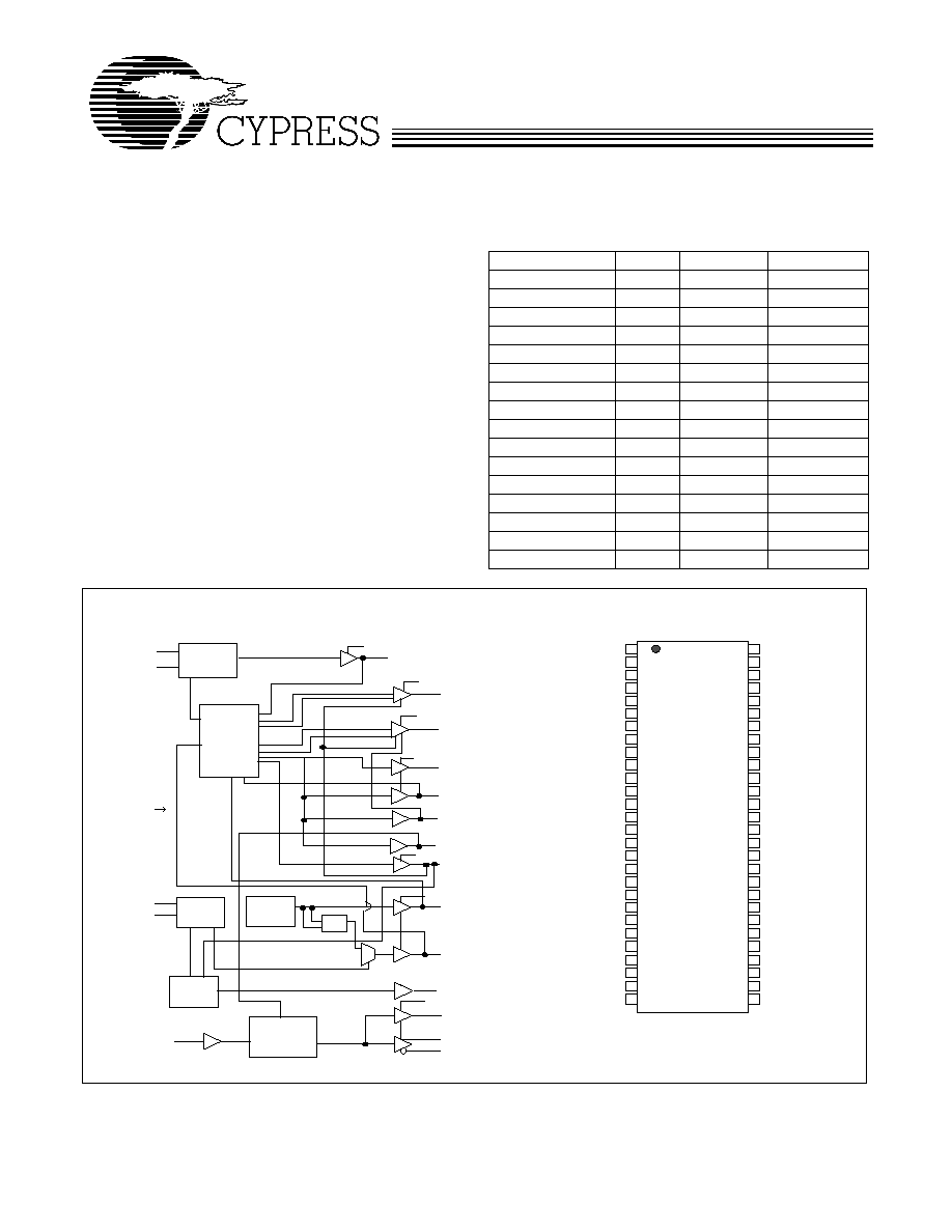
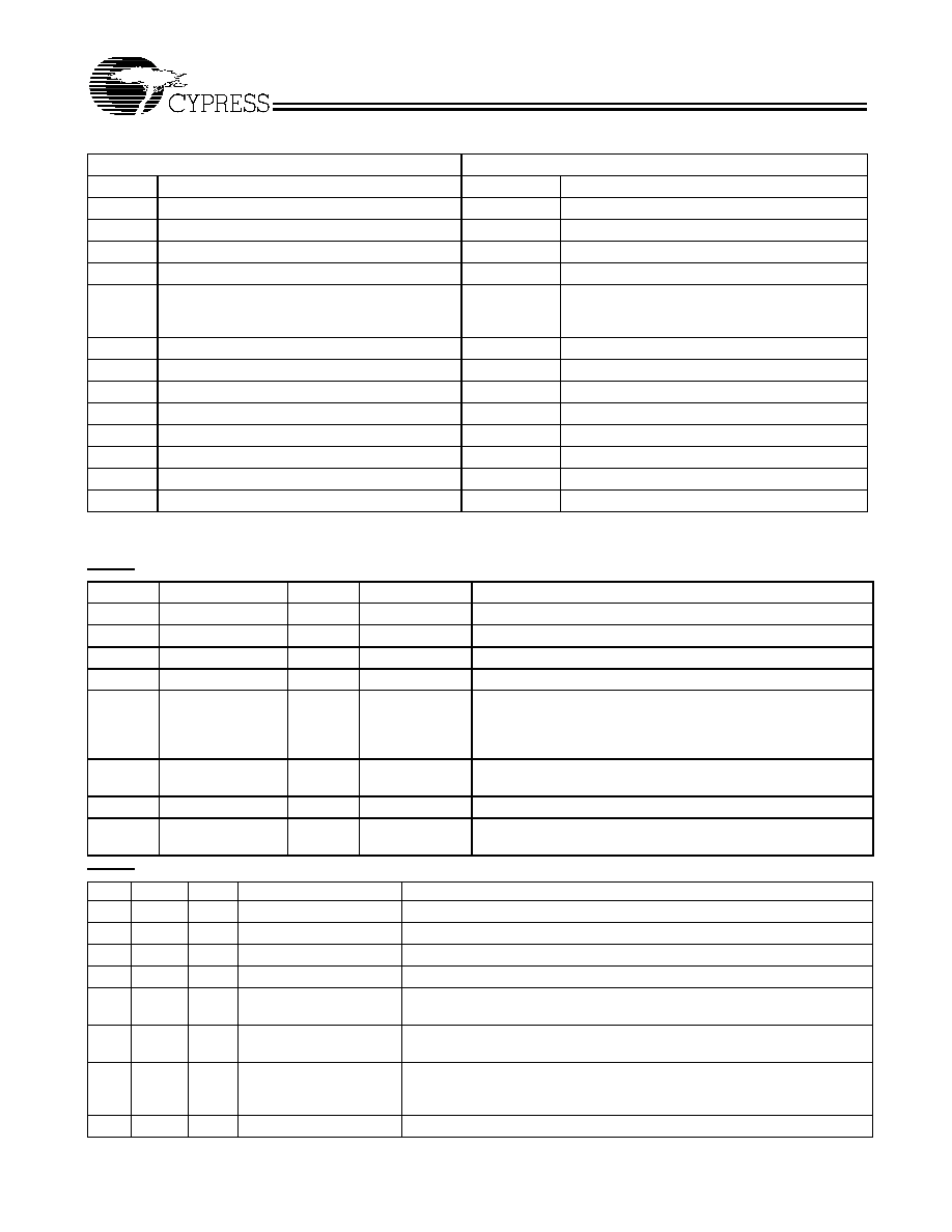
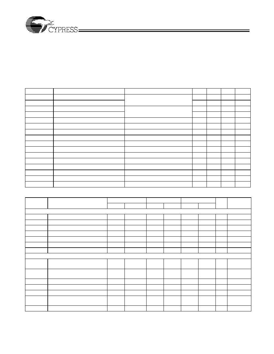
Table 1. Frequency Selection Table
FS(3:0)
CPU
AGP
PCI
0000
66.80
66.80
33.40
0001
100.00
66.80
33.40
0010
120.00
60.00
30.00
0011
133.33
66.67
33.33
0100
72.00
72.00
36.00
0101
105.00
70.00
35.00
0110
160.00
64.00
32.00
0111
140.00
70.00
35.00
1000
77.00
77.00
38.50
1001
110.00
73.33
36.67
1010
180.00
60.00
30.00
1011
150.00
60.00
30.00
1100
90.00
60.00
30.00
1101
100.00
66.67
33.33
1100
200.00
66.67
33.33
1111
133.33
66.67
33.33
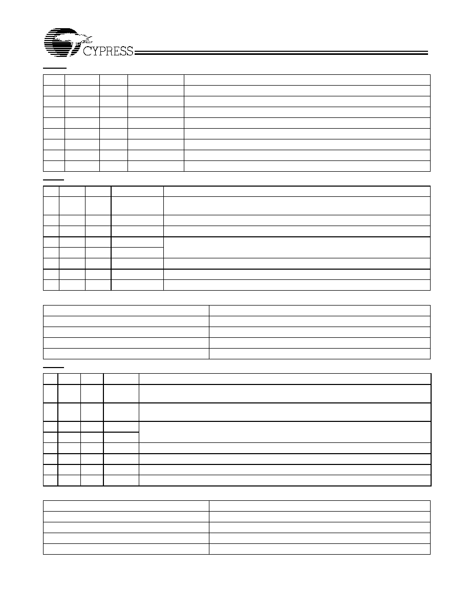
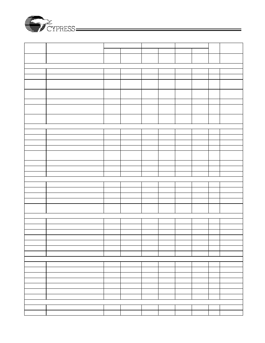
Block Diagram
Pin Configuration
[
1]
PLL1
S2D
CONVERT
SMBus
WD
CPUCS_T/C
VDDC
VDDI
CPU(0:1)/CPU0D_T/C
SELP4_K7#
PCI(3:6)
PCI_F
FS1
REF(0:1)
VDDR
FS0
48M
24_48M
FBOUT
DDRT(0:5)/SDRAM(0,2,4,6,8,10)
SCLK
SDATA
PD#
AGP(0:2)
VDDAGP
VDD48M
VDDD
XTAL
XOUT
XIN
FS2
PCI2
PCI1
VDDPCI
PLL2
SRESET#
/ 2
Buf_IN
REF0
FS3
MULTSEL
SELSDR_DDR
DDRC(0:5)/SDRAM(1,3,5,7,9,11)
WDEN
56 pin SSOP
VSSR
*FS0/REF0
XIN
XOUT
VDDAGP
AGP0
*SELP4_K7/AGP1
VSSAGP
AGP2
**SELSDR_DDR/PCI1
*MULTSEL/PCI2
VSSPCI
PCI3
PCI4
VDDPCI
PCI5
PCI6
VSS48M
**FS3/48M
**FS2/24_48M
VDD48M
VDD
VSS
IREF
*PD#/SRESET#
SCLK
SDATA
**FS1/PCI_F
VDDR
VTTPW RGD#/REF1
VSSC
CPUT/CPUOD_T
CPUC/CPUOD_C
VDDC
VDDI
CPUCS_T
CPUCS_C
FBOUT
BUF_IN
DDRT0/SDRAM0
DDRC0/SDRAM1
DDRT1/SDRAM2
DDRC1/SDRAM3
VDDD
VSSD
DDRT2/SDRAM4
DDRC2/SDRAM5
DDRT3/SDRAM6
DDRC3/SDRAM7
VDDD
VSSD
DDRT4/SDRAM8
DDRC4/SDRAM9
DDRT5/SDRAM10
DDRC5/SDRAM11
VSSI
C
Y
283
41
8
9
10
11
12
13
14
15
16
17
18
19
20
21
22
23
24
25
26
27
28
1
2
3
4
5
6
7
56
55
54
53
52
51
50
49
48
47
46
45
44
43
42
41
40
39
38
37
36
35
34
33
32
31
30
29
CY28341
Document #: 38-07367 Rev. *A
Page 2 of 21
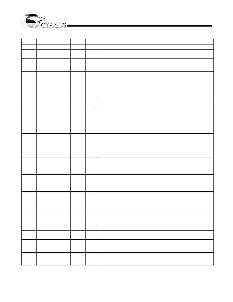
Pin Description
[2]
Pin
Name
PWR
I/O
Description
3
XIN
I
Oscillator Buffer Input. Connect to a crystal or to an external clock.
4
XOUT
VDD
O
Oscillator Buffer Output. Connect to a crystal. Do not connect when an
external clock is applied at X
IN
.
1
FS0/REF0
VDD
I/O
PU
Power-on Bidirectional Input/Output. At power-up, FS0 is the input. When
the power supply voltage crosses the input threshold voltage, FS0 state is
latched and this pin becomes REF0, buffered copy of signal applied at XIN.
56
VTTPWRGD#
VDDR
I
If SELP4_K7 = 1, with a P4 processor setup as CPUT/C. At power-up,
VTT_PWRGD# is an input. When this input transitions to a logic LOW, the FS
(3:0) and MULTSEL are latched and all output clocks are enabled. After the
first HIGH to LOW transition on VTT_PWRGD#, this pin is ignored and will not
effect the behavior of the device thereafter. When the VTT_PWRGD# feature
is not used, please connect this signal to ground through a 10K
resistor.
REF1
VDDR
O
If SELP4_K7 = 0, with an Athlon (K7) processor as CPU_OD(T:C).
VTT_PWRGD# function is disabled, and the feature is ignored. This pin
becomes REF1 and is a buffered copy of the signal applied at X
IN
.
44,42,38,
36,32,30
DDRT
(0:5)/SDRAM(0,2,4,6,
8,10)
VDDD
O
These pins are programmable through strapping pin11, SELSDR_DDR#.If
SELSDR_DDR#.= 0, these pins are configured for DDR clock outputs. They
are "True" copies of signal applied at Pin45, BUF_IN. In this mode, VDDD must
be 2.5VIf SelSDR_DDR#.= 1, these pins are configured for
SDRAM(0,2,4,6,8,10) single ended clock outputs, copies of (and in phase with)
signal applied at Pin45, BUF_IN. In this mode, VDDD must be 3.3V
43,41,37
35,31,29
DDRC
(0:5)/SDRAM(1,3,5,7,
9,11)
VDDD
O
These pins are programmable through strapping pin11, SELSDR_DDR#.If
SelSDR_DDR#.= 0, these pins are configured for DDR clock outputs. They are
"Complementary" copies of signal applied at Pin45, BUF_IN. In this mode,
VDDD must be 2.5VIf SelSDR_DDR#.= 1, these pins are configured for
SDRAM(1,3,5,7,9,11) single-ended clock outputs, copies of (and in phase with)
signal applied at Pin45, BUF_IN. In this mode, VDDD must be 3.3V.
7
SELP4_K7 / AGP1
VDDAG
P
I/O
PU
Power-on Bidirectional Input/Output. At power-up, SELP4_K7 is the input.
When the power supply voltage crosses the input threshold voltage, SELP4_K7
state is latched and this pin becomes AGP1 clock output. SELP4_K7 = 1, P4
mode. SELP4_K7 = 0, K7 mode.
12
MULTSEL / PCI2
VDDPCI
I/O
PU
Power-on Bidirectional Input/Output. At power-up, MULTSEL is the input.
When the power supply voltage crosses the input threshold voltage, MULTSEL
state is latched and this pin becomes PCI2 clock output. MULTSEL = 0, Ioh is
4 x IREFMULTSEL = 1, Ioh is 6 x IREF.
53
CPUT/CPUOD_T
VDDC
O
3.3V CPU Clock outputs. This pin is programmable through strapping pin7,
SELP4_K7. If SELP4_K7 = 1, this pin is configured as the CPUT Clock Output.
If SELP4_K7 = 0, this pin is configured as the CPUOD_T Open Drain Clock
Output. See Table 1.
52
CPUC/CPUOD_C
VDDC
O
3.3V CPU Clock outputs. This pin is programmable through strapping pin7,
SELP4_K7. If SELP4_K7 = 1, this pin is configured as the CPUC Clock Output.
If SELP4_K7 = 0, this pin is configured as the CPUOD_C Open Drain Clock
Output. See Table 1.
48,49
CPUCS_T/C
VDDI
O
2.5V CPU Clock Outputs for Chipset. See Table 1.
14,15,17,
18
PCI (3:6)
VDDPCI
O
PCI Clock Outputs. Are synchronous to CPU clocks. See Table 1.
10
FS1/PCI_F
VDDPCI
I/O
PD
Power-on Bidirectional Input/Output. At power-up, FS0 is the input. When
the power supply voltage crosses the input threshold voltage, FS1 state is
latched and this pin becomes PCI_F clock output.
20
FS3/48M
VDD48M
I/O
PD
Power-on Bidirectional Input/Output. At power-up, FS3 is the input. When
the power supply voltage crosses the input threshold voltage, FS3 state is
latched and this pin becomes 48M, a USB clock output.
CY28341
Document #: 38-07367 Rev. *A
Page 3 of 21
Note:
2.
PU = internal Pull-up. PD = internal Pull-down. Typically = 250 kW (range 200 kW to 500 kW).
11
SELSDR_DDR#/PCI
1
VDDPCI
I/O
PD
Power-on Bidirectional Input/Output. At power-up, SELSDR_DDR is the
input. When the power supply voltage crosses the input threshold voltage,
SELSDR_DDR state is latched and this pin becomes PCI clock
output.SelSDR_DDR#. = 0, DDR Mode. SelSDR_DDR#. = 1, SDR Mode.
21
FS2/24_48M
VDD48M
I/O
PD
Power-on Bidirectional Input/Output. At power-up, FS2 is the input. When
the power supply voltage crosses the input threshold voltage, FS2 state is
latched and this pin becomes 24_48M, a SIO programmable clock output.
6
AGP0
VDDAG
P
O
AGP Clock Output. Is synchronous to CPU clocks. See Table 1.
8
AGP2
VDDAG
P
O
AGP Clock Output. Is synchronous to CPU clocks. See Table 1.
25
IREF
I
Current reference programming input for CPU buffers. A precise resistor is
attached to this pin, which is connected to the internal current reference.
28
SDATA
I/O
Serial Data Input. Conforms to the Philips I2C specification of a Slave
Receive/Transmit device. It is an input when receiving data. It is an open drain
output when acknowledging or transmitting data.
27
SCLK
I
Serial Clock Input. Conforms to the Philips I2C specification.
26
PD#/SRESET#
I/O
PU
Power-down Input/System Reset Control Output. If Byte6 Bit7 = 0, this pin
becomes a SRESET# open drain output, and the internal pulled up is not active.
See system reset description. If Byte6 Bit7 = 1 (default), this pin becomes PD#
input with an internal pull-up. When PD# is asserted LOW, the device enters
power-down mode. See power management function.
45
BUF_IN
If SelSDR_DDR#.= 0, 2.5V CMOS type input to the DDR differential buffers.If
SelSDR_DDR#.= 1, 3.3V CMOS type input to the SDR buffer.
46
FBOUT
If SelSDR_DDR#.= 0, 2.5V single ended SDRAM buffered output of the signal
applied at BUF_IN. It is in phase with the DDRT(0:5) signals.If
SelSDR_DDR#.= 1, 3.3V single ended SDRAM buffered output of the signal
applied at BUF_IN. It is in phase with the SDRAM(0:11) signals
5
VDDAGP
3.3V Power Supply for AGP clocks
51
VDDC
3.3V Power Supply for CPUT/C clocks
16
VDDPCI
3.3V Power Supply for PCI clocks
55
VDDR
3.3V Power Supply for REF clock
50
VDDI
2.5V Power Supply for CPUCS_T/C clocks
22
VDD48M
3.3V Power Supply for 48M
23
VDD
3.3V Common Power Supply
34,40
VDDD
If SelSDR_DDR#.= 0, 2.5V Power Supply for DDR clocksIf SelSDR_DDR#.=
1, 3.3V Power Supply for SDR clocks.
9
VSSAGP
Ground for AGP clocks
13
VSSPCI
Ground for PCI clocks
54
VSSC
Ground for CPUT/C clocks
33,39
VSSD
Ground for DDR clocks
19
VSS48M
Ground for 48M clock
47
VSSI
Ground for ICPUCS_T/C clocks
24
VSS
Common Ground
Pin Description
[2]
(continued)
Pin
Name
PWR
I/O
Description
CY28341
Document #: 38-07367 Rev. *A
Page 4 of 21
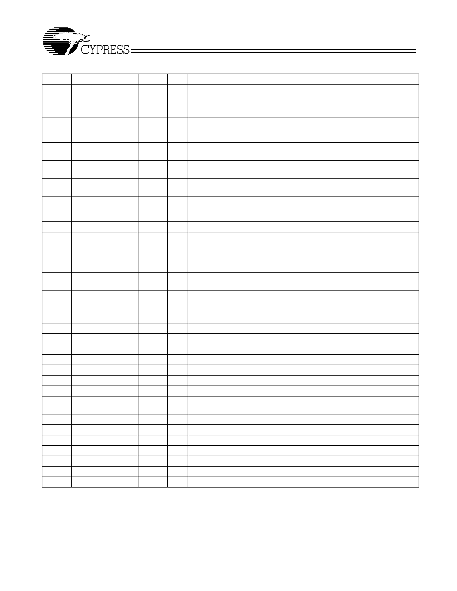
Serial Data Interface
To enhance the flexibility and function of the clock synthesizer,
a two-signal serial interface is provided. Through the Serial
Data Interface, various device functions such as individual
clock output buffers, etc., can be individually enabled or
disabled.
The registers associated with the Serial Data Interface
initializes to their default setting upon power-up, and therefore
use of this interface is optional. Clock device register changes
are normally made upon system initialization, if any are
required. The interface can also be used during system
operation for power management functions.
Data Protocol
The clock driver serial protocol accepts Byte Write, Byte Read,
Block Write, and Block Read operation from the controller. For
Block Write/Read operation, the bytes must be accessed in
sequential order from lowest to highest byte (most significant
bit first) with the ability to stop after any complete byte has
been transferred. For Byte Write and Byte Read operations,
the system controller can access individual indexed bytes. The
offset of the indexed byte is encoded in the command code,
as described in Table 2.
The Block Write and Block Read protocol is outlined in Table 3,
while Table 4 outlines the corresponding Byte Write and Byte
Read protocol. The slave receiver address is 11010010 (D2h).
Table 2. Command Code Definition
Bit
Description
7
0 = Block Read or Block Write operation
1 = Byte Read or Byte Write operation
(6:0)
Byte offset for Byte Read or Byte Write operation. For Block Read or Block Write operations, these bits
should be "0000000"
Table 3. Block Read and Block Write Protocol
Block Write Protocol
Block Read Protocol
Bit
Description
Bit
Description
1
Start
1
Start
2:8
Slave address ≠ 7 bits
2:8
Slave address ≠ 7 bits
9
Write
9
Write
10
Acknowledge from slave
10
Acknowledge from slave
11:18
Command Code ≠ 8-bit "00000000" stands for
Block operation
11:18
Command Code ≠ 8-bit "00000000" stands for
Block operation
19
Acknowledge from slave
19
Acknowledge from slave
20:27
Byte Count ≠ 8 bits
20
Repeat start
28
Acknowledge from slave
21:27
Slave address ≠ 7 bits
29:36
Data byte 0 ≠ 8 bits
28
Read
37
Acknowledge from slave
29
Acknowledge from slave
38:45
Data byte 1 ≠ 8 bits
30:37
Byte count from slave ≠ 8 bits
46
Acknowledge from slave
38
Acknowledge
....
Data Byte N/Slave acknowledge...
39:46
Data byte from slave ≠ 8 bits
....
Data Byte N ≠ 8 bits
47
Acknowledge
....
Acknowledge from slave
48:55
Data byte from slave ≠ 8 bits
....
Stop
56
Acknowledge
....
Data bytes from slave/Acknowledge
....
Data byte N from slave ≠ 8 bits
....
Not Acknowledge
....
Stop
CY28341
Document #: 38-07367 Rev. *A
Page 5 of 21
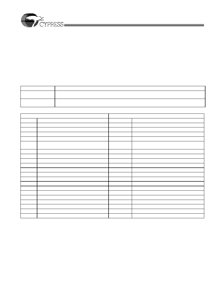
Serial Control Registers
Table 4. Byte Read and Byte Write Protocol
Byte Write Protocol
Byte Read Protocol
Bit
Description
Bit
Description
1
Start
1
Start
2:8
Slave address ≠ 7 bits
2:8
Slave address ≠ 7 bits
9
Write
9
Write
10
Acknowledge from slave
10
Acknowledge from slave
11:18
Command Code ≠ 8 bits "1xxxxxxx" stands for
byte operationbit[6:0] of the command code
represents the offset of the byte to be accessed
11:18
Command Code ≠ 8 bits "1xxxxxxx" stands for
byte operationbit[6:0] of the command code
represents the offset of the byte to be accessed
19
Acknowledge from slave
19
Acknowledge from slave
20:27
Byte Count ≠ 8 bits
20
Repeat start
28
Acknowledge from slave
21:27
Slave address ≠ 7 bits
29
Stop
28
Read
29
Acknowledge from slave
30:37
Data byte from slave ≠ 8 bits
38
Not Acknowledge
39
Stop
Byte 0: Frequency Select Register
Bit
@Pup
Pin#
Name
Description
7
0
Reserved
Reserved
6
H/W Setting
21
FS2
For Selecting Frequencies see Table 1.
5
H/W Setting
10
FS1
For Selecting Frequencies see Table 1.
4
H/W Setting
1
FS0
For Selecting Frequencies see Table 1.
3
0
If this bit is programmed to "1," it enables Write to bits (6:4,1) for
selecting the frequency via software (SMBus). If this bit is
programmed to a "0," it enables only Read of bits (6:4,1), which
reflects the hardware setting of FS(0:3).
2
H/W Setting
11
SELSDR_DDR Only for reading the hardware setting of the SDRAM interface
mode, status of SELSDR_DDR# strapping.
1
H/W Setting
20
FS3
For Selecting frequencies see Table 1
.
0
H/W Setting
7
SELP4_K7
Only for reading the hardware setting of the CPU interface mode,
status of SELP4_K7# strapping.
Byte 1: CPU Clocks Register
Bit
@Pup
Pin#
Name
Description
7
0
MODE
0 = Down Spread. 1 = Center Spread. See Table 9.
6
1
SSCG
1 = Enable (default). 0 = Disable
5
1
SST1
Select spread bandwidth. See Table 9.
4
1
SST0
Select spread bandwidth. See Table 9.
3
1
48,49
CPUCS_T, CPUCS_C
1 = output enabled (running). 0 = output disabled asynchronously in a LOW
state.
2
1
53,52
CPUT/CPUOD_T
CPUC/CPUOD_C
1 = output enabled (running). 0 = output disable.
1
1
53,52
CPUT/C
In K7 mode, this bit is ignored.In P4 mode, 0 = when PD# asserted LOW,
CPUT stops in a HIGH state, CPUC stops in a LOW state. In P4 mode, 1 =
when PD# asserted LOW, CPUT and CPUC stop in High-Z.
0
1
11
MULT0
Only For reading the hardware setting of the Pin11 MULT0 value.
CY28341
Document #: 38-07367 Rev. *A
Page 6 of 21
Byte 2: PCI Clock Register
Bit
@Pup
Pin#
Name
Description
7
0
PCI_DRV
PCI clock output drive strength 0 = Normal, 1 = increase the drive strength 20%.
6
1
10
PCI_F
1 = output enabled (running). 0 = output disabled asynchronously in a LOW state.
5
1
18
PCI6
1 = output enabled (running). 0 = output disabled asynchronously in a LOW state.
4
1
17
PCI5
1 = output enabled (running). 0 = output disabled asynchronously in a LOW state.
3
1
15
PCI4
1 = output enabled (running). 0 = output disabled asynchronously in a LOW state.
2
1
14
PCI3
1 = output enabled (running). 0 = output disabled asynchronously in a LOW state.
1
1
12
PCI2
1 = output enabled (running). 0 = output disabled asynchronously in a LOW state.
0
1
11
PCI1
1 = output enabled (running). 0 = output disabled asynchronously in a LOW state.
Byte 3: AGP/Peripheral Clocks Register
Bit
@Pup
Pin#
Name
Description
7
0
21
24_48M
"0" = pin21 output is 24MHz. Writing a "1" into this register asynchronously changes the
frequency at pin21 to 48 MHz.
6
1
20
48MHz
1 = output enabled (running). 0 = output disabled asynchronously in a LOW state.
5
1
21
24_48M
1 = output enabled (running). 0 = output disabled asynchronously in a LOW state.
4
0
6,7,8
DASAG1
Programming these bits allow shifting skew of the AGP(0:2) signals relative to their
default value. See Table 5.
3
0
6,7,8
DASAG0
2
1
8
AGP2
1 = output enabled (running). 0 = output disabled asynchronously in a LOW state.
1
1
7
AGP1
1 = output enabled (running). 0 = output disabled asynchronously in a LOW state.
0
1
6
AGP0
1 = output enabled (running). 0 = output disabled asynchronously in a LOW state.
Table 5. Dial-a-SkewTM AGP(0:2)
DASAG (1:0)
AGP(0:2) Skew Shift
00
Default
01
≠280 ps
10
+280 ps
11
+480 ps
Byte 4: Peripheral Clocks Register
Bit @Pup Pin#
Name
Description
7
1
20
48M
1 = normal strength, 0 = high strength
1 = normal strength, 0 = high strength
6
1
21
24_48M
1 = normal strength, 0 = high strength
1 = normal strength, 0 = high strength
5
0
6,7,8
DARAG1 Programming these bits allow modifying the frequency ratio of the AGP(2:0), PCI(6:1, F) clocks
relative to the CPU clocks. See Table 6.
4
0
6,7,8
DARAG0
3
1
1
REF0
1 = output enabled (running). 0 = output disabled asynchronously in a LOW state.
2
1
56
REF1
1 = output enabled (running). 0 = output disabled asynchronously in a LOW state. (K7 Mode only.)
1
1
1
REF0
1 = normal strength, 0 = high strength
0
1
56
REF1
1 = normal strength, 0 = high strength (K7 Mode only.)
Table 6. Dial-A-RatioTM AGP(0:2)
DARAG (1:0)
CU/AGP Ratio
00
Frequency Selection Default
01
2/1
10
2.5/1
11
3/1
CY28341
Document #: 38-07367 Rev. *A
Page 7 of 21
Byte 5: SDR/DDR Clock Register
Bit
@Pup
Pin#
Name
Description
7
0
45
BUF_IN
threshold
voltage
DDR Mode, BUF_IN threshold setting. 0 = 1.15V, 1 = 1.05VSDR Mode, BUF_IN
threshold setting. 0 = 1.35V, 1 = 1.25V
6
1
46
FBOUT
1 = output enabled (running). 0 = output disabled asynchronously in a LOW state.
5
1
29,30
DDRT/C5/SD
RAM(10,11)
1 = output enabled (running). 0 = output disabled asynchronously in a LOW state.
4
1
31,32
DDRT/C4/SD
RAM(8,9)
1 = output enabled (running). 0 = output disabled asynchronously in a LOW state.
3
1
35,36
DDRT/C3/SD
RAM(6,7)
1 = output enabled (running). 0 = output disabled asynchronously in a LOW state.
2
1
37,38
DDRT/C2/SD
RAM(4,5)
1 = output enabled (running). 0 = output disabled asynchronously in a LOW state.
1
1
41,42
DDRT/C1/SD
RAM(2,3)
1 = output enabled (running). 0 = output disabled asynchronously in a LOW state.
0
1
43,44
DDRT/C0/SD
RAM(0,1)
1 = output enabled (running). 0 = output disabled asynchronously in a LOW state.
Byte 6: Watchdog Register
Bit @Pup Pin#
Name
Description
7
1
26
SRESET# 1 = Pin 26 is the input pin as PD# signal. 0 = Pin 26 is the output pin as SRESET# signal.
6
0
Frequency
Revert
This bit allows setting the Revert Frequency once the system is rebooted due to Watchdog time
out only.0 = selects frequency of existing H/W setting1 = selects frequency of the second to
last S/W setting (the software setting prior to the one that caused a system reboot).
5
0
WDTEST
WD-Test, ALWAYS program to "0."
4
0
WD Alarm This bit is set to "1" when the Watchdog times out. It is reset to "0" when the system clears the
WD time stamps (WD3:0).
3
0
WD3
This bit allows the selection of the time stamp for the Watchdog timer. See Table 7.
2
0
WD2
This bit allows the selection of the time stamp for the Watchdog timer. See Table 7.
1
0
WD1
This bit allows the selection of the time stamp for the Watchdog timer. See Table 7.
0
0
WD0
This bit allows the selection of the time stamp for the Watchdog timer. See Table 7.
Table 7. Watchdog Time Stamp
WD3
WD2
WD1
WD0
FUNCTION
0
0
0
0
Off
0
0
0
1
1 second
0
0
1
0
2 seconds
0
0
1
1
3 seconds
0
1
0
0
4 seconds
0
1
0
1
5 seconds
0
1
1
0
6 seconds
0
1
1
1
7 seconds
1
0
0
0
8 seconds
1
0
0
1
9 seconds
1
0
1
0
10 seconds
1
0
1
1
11 seconds
1
1
0
0
12 seconds
1
1
0
1
13 seconds
1
1
1
0
14 seconds
1
1
1
1
15 seconds
CY28341
Document #: 38-07367 Rev. *A
Page 8 of 21
Dial-a-Frequency Feature
SMBus Dial-a-Frequency feature is available in this device via
Byte7 and Byte9. P is a PLL constant that depends on the
frequency selection prior to accessing the Dial-a-Frequency
feature.
Spread Spectrum Clock Generation (SSCG)
Spread Spectrum is enabled/disabled via SMBus register
Byte 1, Bit 7.
Byte 7: Dial-a-Frequency Control Register N
Bit
@Pup
Pin#
Name
Description
7
0
Reserved
Reserved for device function test.
6
0
N6, MSB
These bits are for programming the PLL's internal N register. This access
allows the user to modify the CPU frequency at very high resolution
(accuracy). All other synchronous clocks (clocks that are generated from
the same PLL, such as PCI) remain at their existing ratios relative to the
CPU clock.
5
0
N5
4
0
N4
3
0
N3
2
0
N2
1
0
N3
0
0
N0, LSB
Byte 8: Silicon Signature Register (All bits are Read-only)
Bit
@Pup
Pin#
Name
Description
7
0
Revision_ID3
Revision ID bit [3]
6
0
Revision_ID2
Revision ID bit [2]
5
0
Revision_ID1
Revision ID bit [1]
4
0
Revision_ID0
Revision ID bit [0]
3
1
Vender_ID3
Cypress Vender ID bit [3].
2
0
Vender_ID2
Cypress Vender ID bit [2].
1
0
Vender_ID1
Cypress Vender ID bit [1].
0
0
Vender_ID0
Cypress Vender ID bit [0].
Byte9: Dial-A-Frequency Control Register R
Bit @Pup
Pin#
Name
Description
7
0
Reserved
6
0
R5, MSB
These bits are for programming the PLL's internal R register. This access allows the user to
modify the CPU frequency at very high resolution (accuracy). All other synchronous clocks
(clocks that are generated from the same PLL, such as PCI) remain at their existing ratios
relative to the CPU clock.
5
0
R4
4
0
R3
3
0
R2
2
0
R1
1
0
R0
0
0
DAF_ENB This Edge-trigger bit enables the Dial-a-Frequency N and R bits. It is the transition of this bit
from "0" to "1" that latches the N(6:0) and R(5:0) data into the internal N and R registers. The
user must only program a one time "1" into this bit for every new N and R values
Table 8.
FS(4:0)
P
XXXXX
96016000

CY28341
Document #: 38-07367 Rev. *A
Page 9 of 21
System Self-recovery Clock Management
This feature is designed to allow the system designer to
change frequency while the system is running and reboot the
operation of the system in case of a hang-up due to the
frequency change.
When the system sends an SMBus command requesting a
frequency change through Byte 4 or through Bytes 13 and 14,
it must have previously sent a command to Byte 12, for
selecting which time out stamp the Watchdog must perform,
otherwise the System Self Recovery feature will not be appli-
cable. Consequently, this device will change frequency and
then the Watchdog timer starts timing. Meanwhile, the system
BIOS is running its operation with the new frequency. If this
device receives a new SMBus command to clear the bits origi-
nally programmed in Byte 12,Bits (3:0) (reprogram to 0000),
before the Watchdog times out, then this device will keep
operating in its normal condition with the new selected
frequency. If the Watchdog times out the first time before the
new SMBus reprograms Byte12,Bits (3:0) to (0000), then this
device will send a low system reset pulse, on SRESET# (see
Byte12,Bit7), and changes WD alarm (Byte12,Bit4) status to
"1" then restarts the Watchdog timer again. If the Watchdog
times out a second time, then this device will send another low
pulse on SRESET#, will relatch original hardware strapping
frequency (or second to last software selected frequency, see
Byte12,Bit6) selection, set WD alarm bit (Byte12,Bit4) to "1,"
then start WD timer again. The above-described sequence will
keep repeating until the BIOS clears the SMBus
Byte12,Bits(3:0). Once the BIOS sets Byte12,Bits(3:0) = 0000,
then the Watchdog timer is turned off and the WD alarm bit
(Byte12,Bit4) is reset to"0."
Power Management Functions
All clocks can be individually enabled or stopped via the 2-wire
control interface. All clocks are stopped in the LOW state. All
clocks maintain a valid HIGH period on transitions from
running to stop and on transitions from stopped to running
when the chip was not powered down. On power-up, the
VCOs will stabilize to the correct pulse widths within about 0.5
mS.
Table 9. Spread Spectrum Table
Mode
SST1
SST0
% Spread
0
0
0
≠1.5%
0
0
1
≠1.0%
0
1
0
≠0.7%
0
1
1
≠0.5%
1
0
0
Ī0.75%
1
0
1
Ī0.5%
1
1
0
Ī0.35%
1
1
1
Ī0.25%
Swing Select Functions Through Hardware
MULT-
SEL
Board Target
Trace/Term Z
Reference R,
IREF = VDD/(3*Rr)
Output
Current VOH@Z
0
50 Ohm
Rr = 221 1%,
IREF = 5.00 mA
IOH = 4 *
Iref
1.0V@50
1
50 Ohm
Rr = 475 1%,
IREF = 2.32 mA
IOH = 6 *
Iref
0.7V@50
S y s t e m r u n n i n g w i t h
o r i g i n a l l y s e l e c t e d
f r e q u e n c y v i a
h a r d w a r e s t r a p p i n g .
R e c e i v e F r e q u e n c y
C h a n g e R e q u e s t v i a
S M B u s B y t e 4 o r V i a D i a l -
a - f r e q u e n c y ?
S t a r t i n t e r n a l w a t c h d o g t i m e r .
W a t c h D o g t i m e o u t ?
T u r n o f f w a t c h d o g t i m e r .
K e e p n e w f r e q u e n c y s e t t i n g . S e t W D a l a r m
b i t ( b y t e 1 2 , b i t 4 ) t o ' ' 0 '
1 ) S e n d a n o t h e r 3 m S l o w p u l s e o n S R E S E T
2 ) R e l a t c h o r i g i n a l h a r d w a r e s t r a p p i n g s e l e c t i o n
f o r r e t u r n t o o r i g i n a l f r e q u e n c y s e t t i n g s .
3 ) S e t W D A l a r m b i t ( b y t e 1 2 , B i t 4 ) t o " 1 "
4 ) S t a r t W D t i m e r
F r e q u e n c y w i l l c h a n g e b u t S y s t e m S e l f
R e c o v e r y n o t a p p l i c a b l e ( n o t i m e s t a m p
s e l e c t e d a n d b y t e 1 2 , b i t ( 3 : 0 ) i s s t i l l =
" 0 0 0 0 "
N o
N o
Y e s
N o
N o
Y e s
S M B u s b y t e 1 2 t i m e
o u t s t a m p d i s a b l e d ?
I s S M B u s B y t e 9 , t i m e o u t
s t a m p e n a b l e d - ( b y t e 1 2 , b i t
( 3 : 0 ) 0 0 0 0 ) ?
C h a n g e t o a n e w
f r e q u e n c y
Y e s
1 ) S e n d S R E S E T
p u l s e
2 ) S e t W D b i t
( b y t e 1 2 , b i t 4 ) t o ' 1 '
3 ) S t a r t W D t i m e r
Y e s
W a t c h D o g t i m e o u t ?
N o
Y e s
S M B u s b y t e 9 t i m e o u t
s t a m p d i s a b l e d , B y t e
1 2 , b i t ( 3 : 0 ) = ( 0 0 0 0 ) ?
Y e s
N o
Figure 1.
CY28341
Document #: 38-07367 Rev. *A
Page 10 of 21
Maximum Ratings
[3]
Input Voltage Relative to V
SS
:.............................. V
SS
≠ 0.3V
Input Voltage Relative to V
DDQ
or AV
DD
: ............. V
DD
+ 0.3V
Storage Temperature: ................................ ≠65
į
C to + 150
į
C
Operating Temperature: .................................... 0
į
C to +70
į
C
Maximum ESD .............................................................2000V
Maximum Power Supply: ................................................5.5V
This device contains circuitry to protect inputs against damage
due to high-static voltages or electric field. However, precau-
tions should be take to avoid application of any voltage higher
than the maximum-rated voltages to this circuit. For proper
operation, V
IN
and V
OUT
should be constrained to the range:
V
SS
< (V
IN
or V
OUT
) < V
DD
.
Unused inputs must always be tied to an appropriate logic
voltage level (either V
SS
or V
DD
).
DC Parameters
V
DD
= V
DDPCI
= V
DDAGP
= V
DDR
= V
DD48M
= V
DDC
= 3.3V Ī 5%, V
DDI
= V
DD
= 2.5V Ī 5%, T
A
= 0įC to +70įC
Parameter
Description
Conditions
Min.
Typ.
Max.
Unit
VIL1
Input Low Voltage
Applicable to PD#, F S(0:4)
0.8
Vdc
VIH1
Input High Voltage
2.0
Vdc
VIL2
Input Low Voltage
Applicable to SDATA and SCLK
1.0
Vdc
VIH2
Input High Voltage
2.2
Vdc
Vol
Output Low Voltage for SRESET#
I
OL
0.4
V
Iol
Pull-down Current for SRESET#
V
OL
= 0.4V
24
35
mA
Ioz
Three-state Leakage Current
10
Ķ
A
Idd3.3V
Dynamic Supply Current
CPU Frequency Set at 133.3 MHz
[5]
150
190
mA
Idd2.5V
Dynamic Supply Current
CPU Frequency Set at 133.3 MHz
[5]
175
195
mA
Ipd
Power-down Supply Current
PD# = 0
95
600
Ķ
A
Ipup
Internal Pull-up Device Current
Input @ V
SS
≠25
Ķ
A
Ipdwn
Internal Pull-down Device Current
Input @ V
DD
10
Ķ
A
Cin
Input Pin Capacitance
5
pF
Cout
Output Pin Capacitance
6
pF
Lpin
Pin Inductance
7
pF
Cxtal
Crystal Pin Capacitance
Measured from the X
IN
or X
OUT
to V
SS
27
36
45
pF
AC Parameters
Parameter
Description
100 MHz
133MHz
200 MHz
Unit
Notes
[4]
Min.
Max.
Min.
Max
Min.
Max
XTAL
TDC
X
IN
Duty Cycle
45
55
45
55
45
55
%
7,8
TPeriod
X
IN
Period
69.841
71.0
69.84
71.0
69.84
71.0
ns
7,8
VHIGH
X
IN
High Voltage
0.7V
DD
V
DD
0.7V
DD
V
DD
0.7V
DD
V
DD
V
9
VLOW
X
IN
Low Voltage
0
0.3V
DD
0
0.3V
DD
0
0.3V
DD
V
10
Tr/Tf
X
IN
Rise and Fall Times
10.0
10
10
ns
10
TCCJ
X
IN
Cycle to Cycle Jitter
500
500
500
ps
11,12
Txs
Crystal Start-up Time
30
30
30
ms
12,9
P4 Mode CPU at 0.7V
TDC
CPUT/C Duty Cycle
45
55
45
55
45
55
%
7,11,14,21,
22
TPeriod
CPUT/C Period
9.85
10.2
7.35
7.65
4.85
5.1
ns
7,11,14,21,
22
Tr/Tf
CPUT/C Rise and Fall Times
175
700
175
700
175
700
ps
23,24
Rise/Fall Matching
20%
20%
20%
23,26,24
Delta Tr/Tf Rise/Fall Time Variation
125
125
125
ps
11,23,22
TSKEW
CPUCS_T/C to CPUT/C Clock
Skew
0
200
0
150
0
200
ps
11,15,21,22
TCCJ
CPUT/C Cycle to Cycle Jitter
≠150
+150
≠150
+150
≠200
+200
ps
11,15,21,22
Notes:
3.
Multiple Supplies: The Voltage on any input or I/O pin cannot exceed the power pin during power-up. Power supply sequencing is NOT required.
4.
All notes for this table may be found at the end of the table, on page 12.
CY28341
Document #: 38-07367 Rev. *A
Page 11 of 21
Vcross
Crossing Point Voltage at 0.7V
Swing
280
430
280
430
280
430
mV
22
P4 Mode CPU at 1.0V
TDC
CPUT/C Duty Cycle
45
55
45
55
45
55
%
11,14,21
TPeriod
CPUT/C Period
9.85
10.2
7.35
7.65
4.85
5.1
nS
11,14,21
Differential
Tr/Tf
CPUT/C Rise and Fall Times
175
467
175
467
175
467
ps
13,15,25
TSKEW
CPUCS_T/C to CPUT/C Clock
Skew
0
200
0
150
0
200
0
11,15,21
TCCJ
CPUT/C Cycle to Cycle Jitter
≠150
+150
≠150
+150
≠200
+200
ps
11,15,21
Vcross
Crossing Point Voltage at 1V
Swing
510
760
510
760
510
760
mV
26
SE-
DeltaSlew
Absolute Single-ended Rise/Fall
Waveform Symmetry
325
325
325
ps
24,31
K7 Mode
TDC
CPUOD_T/C Duty Cycle
45
55
45
55
45
55
%
11,14
TPeriod
CPUOD_T/C Period
9.98
10.5
7.5
8.0
5
5.5
ns
11,14
TLOW
CPUOD_T/C LOW Time
2.8
1.67
2.8
ns
11,14
Tf
CPUOD_T/C Fall Time
0.4
1.6
0.4
1.6
0.4
1.6
ns
11,13
TSKEW
CPUCS_T/C to CPUT/C Clock
Skew
0
200
0
150
0
200
0
11,15,21
TCCJ
CPUOD_T/C Cycle to Cycle Jitter
≠150
+150
≠150
+150
≠200
+200
ps
11,14
VD
Differential Voltage AC
0.4
Vp+.6V
0.4
Vp+.6V
0.4
Vp+.6V
V
20
VX
Differential Crossover Voltage
500
1100
500
1100
500
1100
mV
19
CHIPSET CLOCK
TDC
CPUCS_T/C Duty Cycle
45
55
45
55
45
55
%
7,11,14
TPeriod
CPUCS_T/C Period
10.0
10.5
15
15.5
10.0
10.5
ns
7,11,14
Tr / Tf
CPUCS_T/C Rise and Fall Times
0.4
1.6
0.4
1.6
0.4
1.6
ns
7,11,13
VD
Differential Voltage AC
0.4
Vp+.6V
0.4
Vp+.6V
0.4
Vp+.6V
V
27
VX
Differential Crossover Voltage
0.5*V
DDI
≠ 0.2
0.5*V
DDI
+
0.2
0.5*V
DDI
≠ 0.2
0.5*V
DDI
+ 0.2
0.5*V
DDI
≠ 0.2
0.5*V
DDI
+ 0.2
V
21
AGP
TDC
AGP(0:2) Duty Cycle
45
55
45
55
45
55
%
7,11,14
TPeriod
AGP(0:2) Period
15
16
15
16
15
16
ns
7,11,14
THIGH
AGP(0:2) HIGH Time
5.25
5.25
5.25
ns
11,16
TLOW
AGP(0:2) LOW Time
5.05
5.05
5.05
ns
11,17
Tr / Tf
AGP(0:2) Rise and Fall Times
0.4
1.6
0.4
1.6
0.4
1.6
ns
11,13
TSKEW
Any AGP to Any AGP clock Skew
250
250
250
ps
11,15
TCCJ
AGP(0:2) Cycle to Cycle Jitter
500
500
500
ps
11,14,15
PCI
TDC
PCI(_F,1:6) Duty Cycle
45
55
45
55
45
55
%
7,11,14
TPeriod
PCI(_F,1:6) Period
30.0
30.0
30.0
ns
7,11,14
THIGH
PCI(_F,1:6) HIGH Time
12.0
12.0
12.0
ns
11,16
TLOW
PCI(_F,1:6) LOW Time
12.0
12.0
12.0
ns
11,17
Tr / Tf
PCI(_F,1:6) Rise and Fall Times
0.5
2.5
0.5
2.5
0.5
2.5
ns
11,13
TSKEW
Any PCI to Any PCI Clock Skew
500
500
500
ps
11,15
TCCJ
PCI(_F,1:6) Cycle to Cycle Jitter
500
500
500
ps
11,14,15
48MHz
TDC
48MHz Duty Cycle
45
55
45
55
45
55
%
7,11,14
TPeriod
48MHz Period
20.8299
20.8333
20.8299 20.8333 20.8299 20.8333
ns
7,11,14
AC Parameters
(continued)
Parameter
Description
100 MHz
133MHz
200 MHz
Unit
Notes
[4]
Min.
Max.
Min.
Max
Min.
Max
CY28341
Document #: 38-07367 Rev. *A
Page 12 of 21
Tr / Tf
48MHz Rise and Fall Times
1.0
4.0
1.0
4.0
1.0
4.0
ns
11,13
TCCJ
48MHz Cycle to Cycle Jitter
500
500
500
ps
11,14,15
24MHz
TDC
24MHz Duty Cycle
45
55
45
55
45
55
%
7,11,14
TPeriod
24MHz Period
41.660
41.667
41.660
41.667
41.660
41.667
ns
7,11,14
Tr / Tf
24MHz Rise and Fall Times
1.0
4.0
1.0
4.0
1.0
4.0
ns
11,13
TCCJ
24MHz Cycle to Cycle Jitter
500
500
500
ps
11,14,15
REF
TDC
REF Duty Cycle
45
55
45
55
45
55
%
7,11,14
TPeriod
REF Period
69.8413
71.0
69.8413
71.0
69.8413
71.0
ns
7,11,14
Tr / Tf
REF Rise and Fall Times
1.0
4.0
1.0
4.0
1.0
4.0
ns
11,13
TCCJ
REF Cycle to Cycle Jitter
1000
1000
1000
ps
11,14,15
DDR
VX
Crossing Point Voltage of
DDRT/C
0.5*V
DD
≠
0.2
0.5*V
DDD
+
0.2
0.5*V
DDD
≠ 0.2
0.5*V
DDD
+ 0.2
0.5*V
DDD
≠0.2
0.5*V
DDD
+0.2
V
19
VD
Differential Voltage Swing
0.7
V
DDD
+ 0.6
0.7
V
DDD
+
0.6
0.7
V
DDD
+
0.6
V
20
TDC
DDRT/C(0:5) Duty Cycle
45
55
45
55
45
55
%
21
TPeriod
DDRT/C(0:5) Period
9.85
10.2
14.85
15.3
9.85
10.2
ns
21
Tr / Tf
DDRT/C(0:5) Rise/Fall Slew Rate
1
3
1
3
1
3
V/ns
13
TSKEW
DDRT/C to Any DDRT/C Clock
Skew
100
100
100
ps
11,15,21
TCCJ
DDRT/C(0:5) Cycle to Cycle Jitter
Ī75
Ī75
Ī75
ps
11,15,21
THPJ
DDRT/C(0:5) Half-period Jitter
Ī100
Ī100
Ī100
ps
11,15,21
TDelay
BUF_IN to Any DDRT/C Delay
1
4
1
4
1
4
ns
11,14
TSKEW
FBOUT to Any DDRT/CSkew
100
100
100
ps
11,14
tstable
All Clock Stabilization from
Power-up
3
3
3
ms
18
Notes:
5.
All outputs loaded as per maximum capacitive load table.
6.
All outputs are not loaded.
7.
This parameter is measured as an average over a 1-
Ķ
s duration, with a crystal center frequency of 14.31818 MHz.
8.
This is required for the duty cycle on the REF clock out to be as specified. The device will operate reliably with input duty cycles up to 30/70 but the REF clock
duty cycle will not be within data sheet specifications.
9.
When crystal meets minimum 40-ohm device series resistance specification.
10. Measured between 0.2V
DD
and 0.7V
DD
.
11. All outputs loaded as per loading specified in the Table 11.
12. When X
IN
is driven from an external clock source (3.3V parameters apply).
13. Probes are placed on the pins, and measurements are acquired between 0.4V and 2.4V for 3.3V signals and between 0.4V and 2.0V for 2.5V signals, and
between 20% and 80% for differential signals.
14. Probes are placed on the pins, and measurements are acquired at 1.5V for 3.3V signals and at 1.25V for 2.5V, and 50% point for differential signals.
15. This measurement is applicable with Spread ON or spread OFF.
16. Probes are placed on the pins, and measurements are acquired at 2.4V for 3.3V signals and at 2.0V for 2.5V signals)
17. Probes are placed on the pins, and measurements are acquired at 0.4V.
18. The time specified is measured from when all VDD's reach their respective supply rail (3.3V and 2.5V) till the frequency output is stable and operating within
the specifications.
19. The typical value of VX is expected to be 0.5*VDDD (or 0.5*VDDC for CPUCS signals) and will track the variations in the DC level of the same.
20. VD is the magnitude of the difference between the measured voltage level on a DDRT (and CPUCS_T) clock and the measured voltage level on its complementary
DDRC (and CPUCS_C) one.
21. Measured at VX, or where subtraction of CLK-CLK# crosses 0 volts.
22. See Figure 10. for 0.7V loading specification.
23. Measured from Vol=0.175V to Voh=0.525V.
24. Measurements taken from common mode waveforms, measure rise/fall time from 0.41V to 0.86V. Rise/fall time matching is defined as "the instantaneous
difference between maximum clk rise (fall) and minimum clk# fall (rise) time, or minimum clk rise (fall) and maximum clk# fall (rise) time". This parameter is
designed for waveform symmetry.
25. Measurement taken from differential waveform, from -0.35V to +0.35V.
26. Measured in absolute voltage, i.e. single-ended measurement.
27. Measured at VX between the rising edge and the following falling edge of the signal.
28. Measured at VX between the falling edge and the following rising edge of the signal.
29. This parameter is intended to be 0.45*Tperiod(min) for minimum spec. and 0.55*Tperiod(min) for maximum spec.
30. Determined as a fraction of 2*(Trise-Tfall)/(Trise+Tfall).
AC Parameters
(continued)
Parameter
Description
100 MHz
133MHz
200 MHz
Unit
Notes
[4]
Min.
Max.
Min.
Max
Min.
Max

CY28341
Document #: 38-07367 Rev. *A
Page 13 of 21
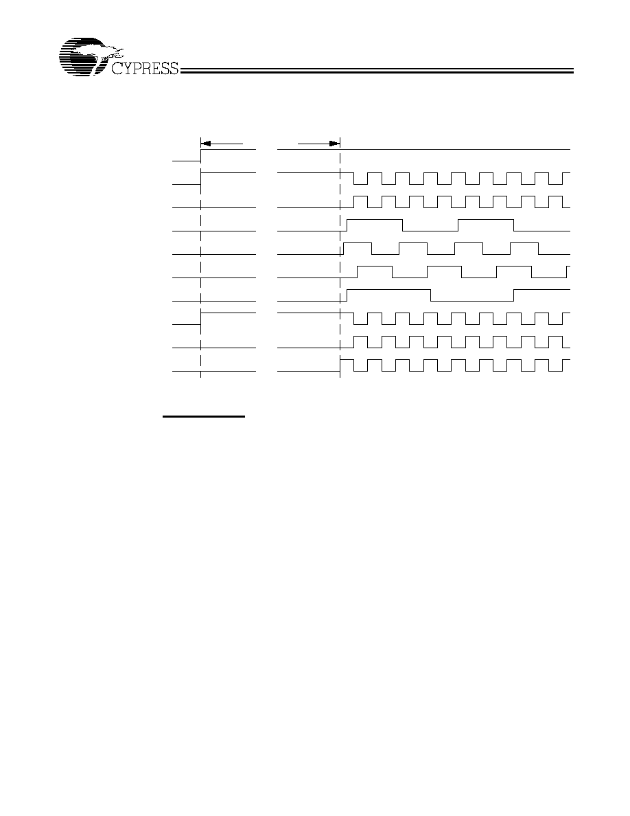
P4 Processor SELP4_K7# = 1
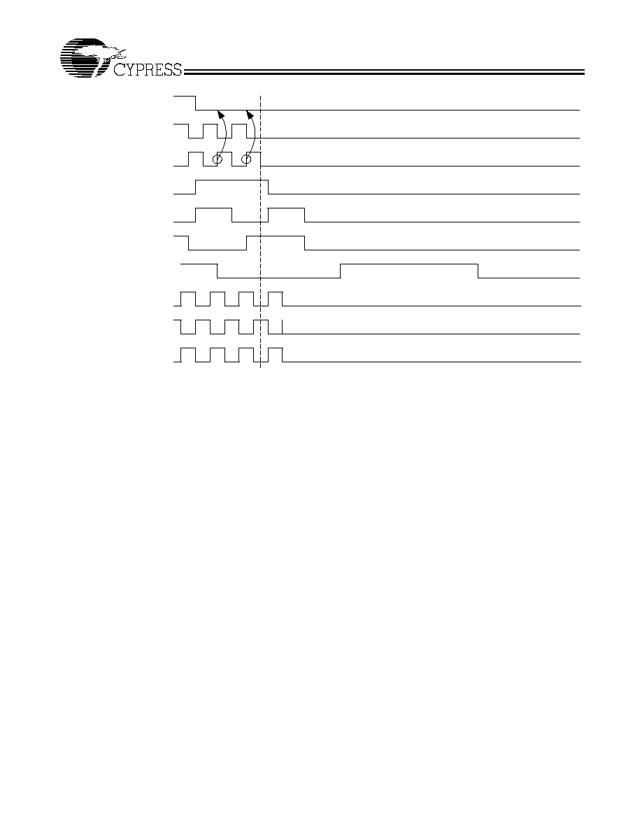
Power-down Assertion (P4 Mode)
When PD# is sampled LOW by two consecutive rising edges
of CPU# clock then all clock outputs except CPU clocks must
be held LOW on their next HIGH to LOW transition. CPU
clocks must be held with the CPU clock pin driven HIGH with
a value of 2 x Iref, and CPU# undriven. Note that Figure 4
shows CPU = 133 MHz, this diagram and description is appli-
cable for all valid CPU frequencies 66, 100, 133, 200MHz.Due
to the state of internal logic, stopping and holding the REF
clock outputs in the LOW state may require more than one
clock cycle to complete.
P C I 3 3 M H z
P W R D W N #
C P U T 1 3 3 M H z
C P U T # 1 3 3 M H z
R E F 1 4 .3 1 8 M H z
U S B 4 8 M H z
S D R A M 1 3 3 M H z
D D R T 1 3 3 M H z
D D R C 1 3 3 M H z
A G P 6 6 M H z
Figure 2. Power-down Assertion Timing Waveform (in P4 Mode)
CY28341
Document #: 38-07367 Rev. *A
Page 14 of 21
Rise and Fall Times
Power-down Deassertion (P4 Mode)
The power-up latency needs to be less than 3 mS.
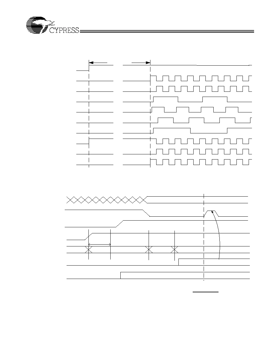
AMD K7 Processor SELP4_K7# = 0
Power-down Assertion (K7 Mode)
When the PD# signal is asserted LOW, all clocks are disabled
to a LOW level in an orderly fashion prior to removing power
from the part. When PD# is asserted (forced) LOW, the device
transitions to a shutdown (power-down) mode and all power
supplies may then be removed. When PD# is sampled LOW
by two consecutive rising edges of CPU clock, then all affected
clocks are stopped in a LOW state as soon as possible. When
in power-down (and before power is removed), all outputs are
synchronously stopped in a LOW state (see figure3 below), all
PLL's are shut off, and the crystal oscillator is disabled. When
the device is shutdown, the I2C function is also disabled.
P C I 3 3 M H z
P W R D W N #
C P U 1 3 3 M H z
C P U # 1 3 3 M H z
A G P 6 6 M H z
R E F 1 4 .3 1 8 M H z
U S B 4 8 M H z
< 1 .5 m s e c
S D R A M 1 3 3 M H z
D D R T 1 3 3 M H z
D D R C 1 3 3 M H z
Figure 3. Power-down Deassertion Timing Waveform (in P4 Mode)
CY28341
Document #: 38-07367 Rev. *A
Page 15 of 21
P C I 3 3M H z
P W R D W N #
R E F 1 4.31 8M H z
U S B 4 8M H z
S D R A M 13 3M H z
D D R T 1 33 M H z
D D R C 13 3M H z
A G P 6 6M H z
C P U O D _ C 1 33M H z
C P U C S _C 1 33M H z
C P U O D _ T 1 33 M H z
C P U C S _T 1 33 M H z
Figure 4. Power-down Assertion Timing Waveform (in K7 Mode)
CY28341
Document #: 38-07367 Rev. *A
Page 16 of 21
Power-down Deassertion (K7 Mode)
When de-asserted PD# to HIGH level, all clocks are enabled
and start running on the rising edge of the next full period in
order to guarantee a glitch-free operation, no partial clock
pulses.
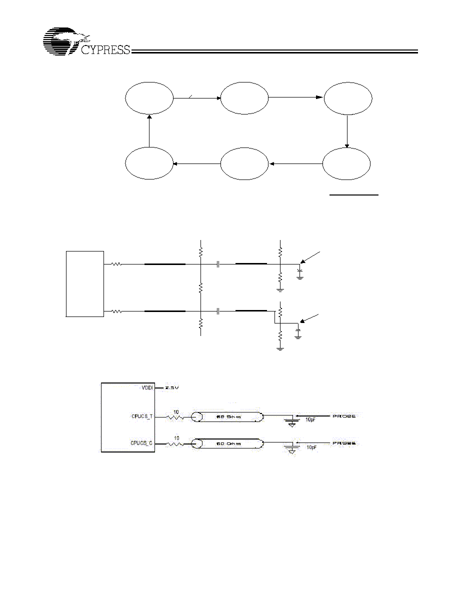
Note:
31. This time diagram shows that VTT_PWRGD# transits to a logic LOW in the first time at power-up. After the first HIGH to LOW transition of VTT_PWRGD#,
device is not affected, VTT_PWRGD# is ignored.
P C I 3 3 M H z
P W R D W N #
C P U 1 3 3 M H z
C P U # 1 3 3 M H z
A G P 6 6 M H z
R E F 1 4 .3 1 8 M H z
U S B 4 8 M H z
< 1 .5 m s e c
S D R A M 1 3 3 M H z
D D R T 1 3 3 M H z
D D R C 1 3 3 M H z
Figure 5. Power-down Deassertion Timing Waveform (in K7 mode)
VID (0:3),
SEL (0,1)
VTT_PW RGD#
PW RGD
VDD Clock Gen
Clock State
Clock Outputs
Clock VCO
0.2-0.3m S
Delay
State 0
State 2
State 3
W ait for
VTT _GD#
Sam ple Sels
Off
Off
On
On
State 1
(Note A)
Figure 6. VTT_PWGD# Timing Diagram (With Advanced PIII Processor SelP4_K7 = 1)
[31]
CY28341
Document #: 38-07367 Rev. *A
Page 17 of 21
Connection Circuit DDRT/C Signals
For Open Drain CPU Output Signals (with K7 Processor SELP4_K7# = 0)
V
T
T
P
W
R
G
D
#
=
L
o
w
D e la y 0 .2 5 m S
S 1
P o w e r O f f
S 0
V D D A = 2 . 0 V
S a m p le
I n p u t s
F S ( 3 : 0 )
S 2
V D D 3 .3 = O f f
N o r m a l
O p e r a t io n
S 3
W a it f o r
1 .1 4 6 m s
E n a b le
O u t p u te s
Figure 7. Clock Generator Power-up/ Run State Diagram (with P4 Processor SELP4_K7# = 1)
Measurement Point
Measurement Point
20 pF
20 pF
680 pF
680 pF
47 Ohm
47 Ohm
52
Ohm
5"
52
Ohm
5"
CPUOD_T
CPUOD_C
VDDCPU(1.5V)
500 Ohm
VDDCPU(1.5V)
500 Ohm
60.4 Ohm
60.4 Ohm
301 Ohm
500 Ohm
500 Ohm
3.3V
3.3V
52
Ohm
1
"
52
Ohm
1"
Figure 8.
6"
6"
Figure 9.
CY28341
Document #: 38-07367 Rev. *A
Page 18 of 21
For Differential CPU Output Signals (with P4 Processor SELP4_K7= 1)
The following diagram shows lumped test load configurations
for the differential Host Clock Outputs.
Note:
32. Ideally the probes should be placed on the pins. If there is a transmission line between the test point and the pin for one signal of the pair (e.g., CPU), the same
length transmission line to the other signal of the pair (e.g., AGP) should be added.
Table 10. Signal Loading Table
Clock Name
Max Load (in pF)
REF (0:1), 48MHz (USB), 24_48MHz
20
AGP(0:2), SDRAM (0:11)
30
PCI_F(0:5)
30
DDRT/C (0:5), FBOUT
CPUT/C
See Figure 10
CPUOD_T/C
See Figure 8
CPUCS_T/C
See Figure 9
CLK Measurement Point
R
ref
R
tA1
CPUT
MULTSEL
CLK Measurement Point
R
LA1
R
D
R
LB1
R
LA2
R
LB2
R
tA2
R
tB1
R
tB2
C
LA
C
LB
T
PCB
T
PCB
CPUT#
Figure 10.
Table 11. Lumped Test Load Configuration
Component 0.7V Amplitude Value 1.0V Amplitude Value
R
tA1
, R
tA2
33
0
R
LA1
, R
LA2
49.9
T
PCB
3" 50
Z
3" 50
Z
R
LB1
, R
LB2
63
R
D
470
R
tB1
, R
tB2
0
33
C
LA
, C
LB
2 pF
2 pF
R
ref
475
w/mult0 = 1
221
w/mult0 = 0
Group Timing Relationships and Tolerances
[32]
Offset (ps) Tolerance (ps) Conditions
t
CSAGP
CPUCS to
AGP
750
500
CPUCS
Leads
t
AP
AGP to
PCI
1,250
500
AGP Leads

CY28341
Document #: 38-07367 Rev. *A
Page 19 of 21
0ns
10ns
20ns
30ns
AGP CLOCK 66.6MHz
PCI CLOCK 33.3MHz
CPU CLOCK 66.6MHz
CPU CLOCK 100MHz
CPU CLOCK 133.3MHz
t
AP
t
CSAGP
Ordering Information
Part Number
Package Type
Product Flow
CY28341OC
56-pin Shrunk Small Outline package (SSOP)
Commercial, 0
į
to 70
į
C
CY28341OCT
56-pin Shrunk Small Outline package (SSOP)≠Tape and Reel
Commercial, 0
į
to 70
į
C
CY28341ZC
56-pin Thin Shrunk Small Outline package (TSSOP)
Commercial, 0
į
to 70
į
C
CY28341ZCT
56-pin Thin Shrunk Small Outline package (TSSOP)≠Tape and Reel
Commercial, 0
į
to 70
į
C

CY28341
Document #: 38-07367 Rev. *A
Page 20 of 21
© Cypress Semiconductor Corporation, 2002. The information contained herein is subject to change without notice. Cypress Semiconductor Corporation assumes no responsibility for the use
of any circuitry other than circuitry embodied in a Cypress Semiconductor product. Nor does it convey or imply any license under patent or other rights. Cypress Semiconductor does not authorize
its products for use as critical components in life-support systems where a malfunction or failure may reasonably be expected to result in significant injury to the user. The inclusion of Cypress
Semiconductor products in life-support systems application implies that the manufacturer assumes all risk of such use and in doing so indemnifies Cypress Semiconductor against all charges.
Package Drawing and Dimensions
Purchase of I2C components from Cypress or one of its sublicensed Associated Companies conveys a license under the Philips
I2C Patent Rights to use these components in an I2C system, provided that the system conforms to the I2C Standard Specification
as defined by Philips. VIA is a trademark of VIA Technologies, Inc. Pentium 4 is a registered trademark of Intel Corporation. Athlon
is a trademark of AMD Corporation, Inc. Dial-a-Frequency, Dial-a-dB, Dial-a-Skew, and Dial-a-Ratio are trademarks of Cypress
Semiconductor. All product and computer names mentioned in this document may be the trademarks of their respective holders.
51-85060-B
56-lead Thin Shrunk Small Outline Package, Type II (6 mm ◊ 12 mm) Z56
56-lead Shrunk Small Outline Package O56
51-85062-C

CY28341
Document #: 38-07367 Rev. *A
Page 21 of 21
Document Title: CY28341 Universal Single-Chip Clock Solution for VIA P4M266/KM266 DDR Systems
Document Number: 38-07367
REV.
ECN NO.
Issue
Date
Orig. of
Change
Description of Change
**
112783
05/28/02
DMG
New Data Sheet
*A
122908
12/26/02
RBI
Add power requirements to maximum ratings information