Clock Synthesizer with Differential CPU Outputs
CY28346-2
Cypress Semiconductor Corporation
∑
3901 North First Street
∑
San Jose
,
CA 95134
∑
408-943-2600
Document #: 38-07509 Rev. *A
Revised June 5, 2003
Features
∑ Compliant with Intel
Æ
CK 408 Mobile Clock Synthesizer
specifications
∑ 3.3V power supply
∑ 3 differential CPU clocks
∑ 10 copies of PCI clocks
∑ 5/6 copies of 3V66 clocks
∑ SMBus support with Read Back capabilities
∑ Spread Spectrum electromagnetic interference (EMI)
reduction
∑ Dial-a-Frequency
features
∑ Dial-a-dBTM features
∑ Extended operating temperature range, 0
∞
C to 85
∞
C
∑ 56-pin TSSOP packages
Note:
1.
TCLK is a test clock driven on the XTAL_IN input during test mode. M = driven to a level between 1.0V and 1.8V. If the S2 pin is at a M level during power-up,
a 0 state will be latched into the devices internal state register.
Table 1. Frequency Table
[1]
S2 S1
S0
CPU
(0:2)
3V66
66BUFF(0:2)/
3V66(0:4)
66IN/
3V66-5
PCIF/PCI
REF
USB/
DOT
1
0
0
66M
66M
66IN
66-MHz clock input
66IN/2
14.318M
48M
1
0
1
100M
66M
66IN
66-MHz clock input
66IN/2
14.318M
48M
1
1
0
200M
66M
66IN
66-MHz clock input
66IN/2
14.318M
48M
1
1
1
133M
66M
66IN
66-MHz clock input
66IN/2
14.318M
48M
0
0
0
66M
66M
66M
66M
33 M
14.318M
48M
0
0
1
100M
66M
66M
66M
33 M
14.318M
48M
0
1
0
200M
66M
66M
66M
33 M
14.318M
48M
0
1
1
133M
66M
66M
66M
33 M
14.318M
48M
M
0
0
Hi-Z
Hi-Z
Hi-Z
Hi-Z
Hi-Z
Hi-Z
Hi-Z
M
0
1
TCLK/2
TCLK/4
TCLK/4
TCLK/4
TCLK/8
TCLK
TCLK/2
PLL1
PLL2
/2
WD
Logic
Power
Up Logic
XIN
XOUT
CPU_STP#
IREF
VSSIREF
S(0:2)
MULT0
VTT_PWRGD#
PCI_STP#
PD#
SDATA
SCLK
VDDA
66B[0:2]/3V66[2:4]
48M_DOT
48M_USB
PCI_F(0:2)
PCI(0:6)
3V66_1/VCH
3V66_0
CPUC(0:2)
CPUT(0:2)
REF
66IN/3V66-5
I2C
Logic
VDD
XIN
XOUT
VSS
PCIF0
PCIF1
PCIF2
VDD
VSS
PCI0
PCI1
PCI2
PCI3
VDD
VSS
PCI4
PCI5
PCI6
VDD
VSS
66B0/3V66_2
66B1/3V66_3
66B2/3V66_4
66IN/3V66_5
PD#
VDDA
VSSA
VTT_PWRGD#
REF
S1
S0
CPU_STP#
CPUT0
CPUC0
VDD
CPUT1
CPUC1
VSS
VDD
CPUT2
CPUC2
MULT0
IREF
VSSIREF
S2
48M_USB
48M_DOT
VDD
VSS
3V66_1/VCH
PCI_STP#
3V66_0
VDD
VSS
SCLK
SDATA
1
2
3
4
5
6
7
8
9
10
11
12
13
14
15
16
17
18
19
20
21
22
23
24
25
26
27
28
56
55
54
53
52
51
50
49
48
47
46
45
44
43
42
41
40
39
38
37
36
35
34
33
32
31
30
29
C
Y
2
834
6-
2
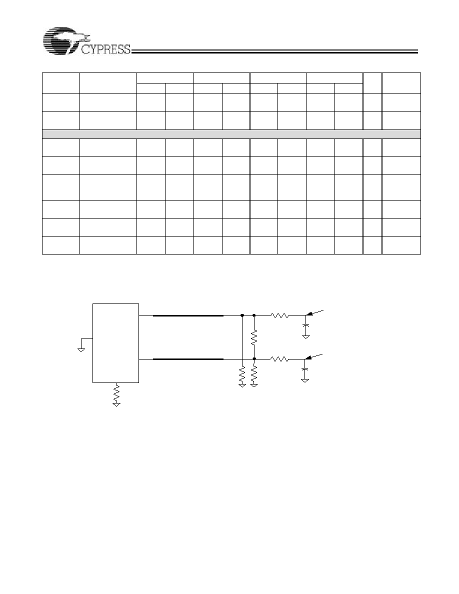
Block Diagram
Pin Configuration
CY28346-2
Document #: 38-07509 Rev. *A
Page 2 of 20
Pin Description
Pin
Name
PWR
I/O
Description
2
XIN
VDD
I
Oscillator Buffer Input. Connect to a crystal or to an external clock.
3
XOUT
VDD
O
Oscillator Buffer Output. Connect to a crystal. Do not connect when an
external clock is applied at XIN.
52, 51, 49, 48,
45, 44
CPUT(0:2),
CPUC(0:2)
VDD
O
Differential host output clock pairs. See Table 1 for frequencies and
functionality.
10, 11, 12, 13,
16, 17, 18
PCI(0:6)
VDDP
O
PCI clock outputs. Are synchronous to 66IN or 3V66 clock. See Table 1.
5, 6, 7
PCIF (0:2)
VDD
O
33-MHz PCI clocks, which are
˜
2 copies of 66IN or 3V66 clocks, may
be free running (not stopped when PCI_STP# is asserted LOW) or
may be stoppable depending on the programming of SMBus
register Byte3, Bits (3:5).
56
REF
VDD
O
Buffered output copy of the device's XIN clock.
42
IREF
VDD
I
Current reference programming input for CPU buffers. A resistor is
connected between this pin and VSSIREF.
28
VTT_PWRGD#
VDD
I
Qualifying input that latches S(0:2) and MULT0. When this input is at
a logic low, the S(0:2) and MULT0 are latched.
39
48M_USB
VDD48
O
Fixed 48-MHz USB clock outputs.
38
48M_DOT
VDD48
O
Fixed 48-MHZ DOT clock outputs.
33
3V66_0
VDD
O
3.3V 66-MHz fixed frequency clock.
35
3V66_1/VCH
VDD
O
3.3V clock selectable with SMBus byte0, Bit5, when Byte5, Bit5.
When Byte 0 Bit 5 is at a logic 1, then this pin is a 48M output clock. When
byte0, Bit5 is a logic 0, then this is a 66M output clock (default).
25
PD#
VDD
I
PU
This pin is a power-down mode pin. A logic LOW level causes the
device to enter a power-down state. All internal logic is turned off except
for the SMBus logic. All output buffers are stopped.
43
MULT0
VDD
I
PU
Programming input selection for CPU clock current multiplier.
55, 54
S(0,1)
I
I
Frequency select inputs. See Table 1
29
SDATA
I
I
Serial data input. Conforms to the SMBus specification of a Slave
Receive/Transmit device. It is an input when receiving data. It is an open
drain output when acknowledging or transmitting data.
30
SCLK
I
I
Serial clock input. Conforms to the SMBus specification.
40
S2
VDD
I
T
Frequency select input. See Table 1. This is a Tri-level input that is
driven HIGH, LOW, or driven to a intermediate level.
34
PCI_STP#
VDD
I
PU
PCI clock disable input. When asserted LOW, PCI (0:6) clocks are
synchronously disabled in a LOW state. This pin does not effect PCIF
(0:2) clocks' outputs if they are programmed to be PCIF clocks via the
device's SMBus interface.
53
CPU_STP#
VDD
I
PU
CPU clock disable input. When asserted LOW, CPUT (0:2) clocks are
synchronously disabled in a HIGH state and CPUC(0:2) clocks are
synchronously disabled in a LOW state.
24
66IN/3V66_5
VDD
I/O
Input connection for 66CLK(0:2) output clock buffers if S2 = 1, or
output clock for fixed 66-MHz clock if S2 = 0. See Table 1.
21, 22, 23
66B(0:2)/
3V66(2:4)
VDD
O
3.3V clock outputs. These clocks are buffered copies of the 66IN clock
or fixed at 66 MHz. See Table 1.
1, 8, 14, 19, 32,
37, 46, 50
VDD
≠
PWR 3.3V power supply.
4, 9, 15, 20, 27,
31, 36, 47
VSS
≠
PWR Common ground.
CY28346-2
Document #: 38-07509 Rev. *A
Page 3 of 20
Serial Data Interface
To enhance the flexibility and function of the clock synthesizer,
a two-signal serial interface is provided. Through the Serial
Data Interface, various device functions, such as individual
clock output buffers, can be individually enabled or disabled.
The registers associated with the Serial Data Interface
initializes to their default setting upon power-up, and therefore
use of this interface is optional. Clock device register changes
are normally made upon system initialization, if any are
required. The interface can also be used during system
operation for power management functions.
Data Protocol
The clock driver serial protocol accepts block write and block
read operations from the controller. For block write/read
operation, the bytes must be accessed in sequential order
from lowest to highest byte (most significant bit first) with the
ability to stop after any complete byte has been transferred.
The block write and block read protocol is outlined in Table 2.
The slave receiver address is 11010010 (D2h).
41
VSSIREF
≠
PWR Current reference programming input for CPU buffers. A resistor is
connected between this pin and IREF. This pin should also be returned
to device VSS.
26
VDDA
≠
PWR Analog power input. Used for PLL and internal analog circuits. It is also
specifically used to detect and determine when power is at an acceptable
level to enable the device to operate.
Pin Description
(continued)
Pin
Name
PWR
I/O
Description
Table 2. Block Read and Block Write Protocol
Block Write Protocol
Block Read Protocol
Bit
Description
Bit
Description
1
Start
1
Start
2:8
Slave address ≠ 7 bits
2:8
Slave address ≠ 7 bits
9
Write = 0
9
Write = 0
10
Acknowledge from slave
10
Acknowledge from slave
11:18
Command Code ≠ 8 bit
`00000000' stands for block operation
11:18
Command Code ≠ 8 bit
`00000000' stands for block operation
19
Acknowledge from slave
19
Acknowledge from slave
20:27
Byte Count ≠ 8 bits
20
Repeat start
28
Acknowledge from slave
21:27
Slave address ≠ 7 bits
29:36
Data byte 1 ≠ 8 bits
28
Read = 1
37
Acknowledge from slave
29
Acknowledge from slave
38:45
Data byte 2 ≠ 8 bits
30:37
Byte count from slave ≠ 8 bits
46
Acknowledge from slave
38
Acknowledge
....
......................
39:46
Data byte from slave ≠ 8 bits
....
Data Byte (N≠1) ≠8 bits
47
Acknowledge
....
Acknowledge from slave
48:55
Data byte from slave ≠ 8 bits
....
Data Byte N ≠8 bits
56
Acknowledge
....
Acknowledge from slave
....
Data bytes from slave/Acknowledge
....
Stop
....
Data byte N from slave ≠ 8 bits
....
Not Acknowledge
....
Stop
CY28346-2
Document #: 38-07509 Rev. *A
Page 4 of 20
Byte 0: CPU Clock Register
Bit @Pup
Name
Description
7
0
Spread Spectrum Enable, 0 = Spread Off, 1 = Spread On. This is a Read and Write control bit.
6
0
CPU clock Power-down Mode Select.
0 = Drive CPUT(0:2) to 4 or 6 IREF and drive CPUC(0:2) to low when PD# is asserted LOW.
1 = Three-state all CPU outputs. This is only applicable when PD# is LOW. It is not applicable to
CPU_STP#.
5
0
3V66_1/VCH
3V66_1/VCH frequency Select, 0 = 66M selected, 1 = 48M selected
This is a Read and Write control bit.
4
Pin 53
CPUT,CPUC
CPU_STP#. Reflects the current value of the external CPU_STP# (pin 53) This bit is Read-only.
3
Pin 34
PCI
Reflects the current value of the internal PCI_STP# function when read. Internally PCI_STP# is
a logical AND function of the internal SMBus register bit and the external PCI_STP# pin.
2
Pin 40
Frequency Select Bit 2. Reflects the value of SEL2 (pin 40). This bit is Read-only.
1
Pin 55
Frequency Select Bit 1. Reflects the value of SEL1 (pin 55). This bit is Read-only.
0
Pin 54
Frequency Select Bit 0. Reflects the value of SEL0 (pin 54). This bit is Read-only.
Byte 1: CPU Clock Register
Bit @Pup
Name
Description
7
Pin 43
MULT0
MULT0 (Pin 43) Value. This bit is Read-only.
6
0
CPU_STP#
Controls functionality of CPUT/C(0:2) outputs when CPU_STP# is asserted. 0 = Drive CPUT(0:2) to
4 or 6 IREF and drive CPUC(0:2) to low when CPU_STP# asserted LOW. 1 = Three-state all CPU
outputs. This bit will override Byte0, Bit6 such that even if it is a 0, when PD# goes low the CPU outputs
will be three-stated.
5
0
CPUT2
CPUC2
Controls CPU2 functionality when CPU_STP# is asserted LOW
1 = Free Running, 0 = Stopped LOW with CPU_STP# asserted LOW
This is a Read and Write control bit.
4
0
CPUT1
CPUC1
Controls CPU1 functionality when CPU_STP# is asserted LOW
1 = Free Running, 0 = Stopped LOW with CPU_STP# asserted LOW
This is a Read and Write control bit.
3
0
CPUT0
CPUC0
Controls CPUT0 functionality when CPU_STP# is asserted LOW
1 = Free Running, 0 = Stopped LOW with CPU_STP# asserted LOW
This is a Read and Write control bit.
2
1
CPUT2
CPUC2
CPUT/C2 Output Control, 1 = enabled, 0 = disable HIGH and CPUC2 disables LOW
This is a Read and Write control bit.
1
1
CPUT1
CPUC1
CPUT/C1 Output Control, 1 = enabled, 0 = disable HIGH and CPUC1 disables LOW
This is a Read and Write control bit.
0
1
CPUT0
CPUC0
CPUT/C0 Output Control, 1 = enabled, 0 = disable HIGH and CPUC0 disables LOW
This is a Read and Write control bit.
Byte 2: PCI Clock Control Register (all bits are read and write functional)
Bit
@Pup
Name
Description
7
0
REF
REF Output Control. 0 = high strength, 1 = low strength
6
1
PCI6
PCI6 Output Control. 1 = enabled, 0 = forced LOW
5
1
PCI5
PCI5 Output Control. 1 = enabled, 0 = forced LOW
4
1
PCI4
PCI4 Output Control. 1 = enabled, 0 = forced LOW
3
1
PCI3
PCI3 Output Control. 1 = enabled, 0 = forced LOW
2
1
PCI2
PCI2 Output Control. 1 = enabled, 0 = forced LOW
1
1
PCI1
PCI1 Output Control. 1 = enabled, 0 = forced LOW
0
1
PCI0
PCI0 Output Control. 1 = enabled, 0 = forced LOW
CY28346-2
Document #: 38-07509 Rev. *A
Page 5 of 20
Byte 3: PCIF Clock and 48M Control Register (all bits are read and write functional)
Bit
@Pup
Name
Description
7
1
48M_DOT
48M_DOT Output Control,1 = enabled, 0 = forced LOW
6
1
48M_USB
48M_USB Output Control,1 = enabled, 0 = forced LOW
5
0
PCIF2
PCI_STP#, control of PCIF2.
0 = Free Running, 1 = Stopped when PCI_STP# is LOW
4
0
PCIF1
PCI_STP#, control of PCIF1.
0 = Free Running, 1 = Stopped when PCI_STP# is LOW
3
0
PCIF0
PCI_STP#, control of PCIF0.
0 = Free Running, 1 = Stopped when PCI_STP# is LOW
2
1
PCIF2
PCIF2 Output Control. 1=running, 0=forced LOW
1
1
PCIF1
PCIF1 Output Control. 1= running, 0=forced LOW
0
1
PCIF0
PCIF0 Output Control. 1= running, 0=forced LOW
Byte 4: DRCG Control Register(all bits are read and write functional)
Bit
@Pup
Name
Description
7
0
SS2 Spread Spectrum control bit (0 = down spread, 1 = center spread)
6
0
Reserved
5
1
3V66_0
3V66_0 Output Enabled. 1 = enabled, 0 = disabled
4
1
3V66_1/VCH
3V66_1/VCH Output Enable. 1 = enabled, 0 = disabled
3
1
3V66_5
3V66_5 Output Enable. 1 = enabled, 0 = disabled
2
1
66B2/3V66_4
66B2/3V66_4 Output Enabled. 1 = enabled, 0 = disabled
1
1
66B1/3V66_3
66B1/3V66_3 Output Enabled. 1 = enabled, 0 = disabled
0
1
66B0/3V66_2
66B0/3V66_2 Output Enabled. 1 = enabled, 0 = disabled
Byte 5: Clock Control Register (all bits are read and write functional)
Bit
@Pup
Name
Description
7
0
SS1 Spread Spectrum control bit
6
1
SS0 Spread Spectrum control bit
5
0
66IN to 66M delay Control MSB
4
0
66IN to 66M delay Control LSB,
3
0
Reserved
2
0
48M_DOT edge rate control. When set to 1, the edge is slowed by 15%.
1
0
Reserved
0
0
USB edge rate control. When set to 1, the edge is slowed by 15%
Byte 6: Silicon Signature Register
[2]
(all bits are read-only)
Bit
@Pup
Name
Description
7
0
6
0
5
0
4
1
3
0
Vendor Code, 011 = IMI
2
0
1
1
0
1
Note:
2.
When writing to this register the device will acknowledge the write operation, but the data itself will be ignored.
CY28346-2
Document #: 38-07509 Rev. *A
Page 6 of 20
Dial-a-Frequency Feature
SMBus Dial-a-Frequency feature is available in this device via
Byte8 and Byte9. See our App Note AN-0025 for details on our
Dial-a-Frequency feature.
P is a large value PLL constant that depends on the frequency
selection achieved through the hardware selectors (S1, S0).
P value may be determined from Table 3.
Dial-a-dB Features
SMBus Dial-a-dB feature is available in this device via Byte8
and Byte9.
Spread Spectrum Clock Generation (SSCG)
Spread Spectrum is a modulation technique used to
minimizing EMI radiation generated by repetitive digital
signals. A clock presents the greatest EMI energy at the center
frequency it is generating. Spread Spectrum distributes this
energy over a specific and controlled frequency bandwidth
therefore causing the average energy at any one point in this
band to decrease in value. This technique is achieved by
modulating the clock away from its resting frequency by a
certain percentage (which also determines the amount of EMI
reduction). In this device, Spread Spectrum is enabled by
setting specific register bits in the SMBus control Bytes.
Table 4 is a listing of the modes and percentages of Spread
Spectrum modulation that this device incorporates.
Byte 7: Watchdog Time Stamp Register
Bit
@Pup
Name
Description
7
0
Reserved
6
0
Reserved
5
0
Reserved
4
0
Reserved
3
0
Reserved
2
0
Reserved
1
0
Reserved
0
0
Reserved
Byte 8: Dial-a-Frequency Control Register N (all bits are read and write functional)
Bit
@Pup
Name
Description
7
0
N7, MSB
6
0
N6
5
0
N5
4
0
N4
3
0
N3
2
0
N2
1
0
N3
0
0
N0, LSB
Byte 9: Dial-a-Frequency Control Register R (all bits are read and write functional)
Bit
@Pup
Name
Description
7
0
R6 MSB
6
0
R5
5
0
R4
4
0
R3
3
0
R2
2
0
R1
1
0
R0, LSB
0
0
R and N register load gate 0 = gate closed (data is latched), 1 = gate open
(data is loading from SMBus registers into R and N)
Table 3. P Value
S(1:0)
P
0 0
32005333
0 1
48008000
1 0
96016000
1 1
64010667

CY28346-2
Document #: 38-07509 Rev. *A
Page 7 of 20
Special Functions
PCIF and IOAPIC Clock Outputs
The PCIF clock outputs are intended to be used, if required,
for systems IOAPIC clock functionality. ANY two of the PCIF
clock outputs can be used as IOAPIC 33-MHz clock outputs.
They are 3.3V outputs will be divided down via a simple
resistive voltage divider to meet specific system IOAPIC clock
voltage requirements. In the event these clocks are not
required, then these clocks can be used as general PCI clocks
or disabled via the assertion of the PCI_STP# pin.
3V66_1/VCH Clock Output
The 3V66_1/VCH pin has a dual functionality that is selectable
via SMBus.
Configured as DRCG (66M), SMBus Byte0, Bit 5 = `0'
The default condition for this pin is to power up in a 66M
operation. In 66M operation this output is SSCG capable and
when spreading is turned on, this clock will be modulated.
Configured as VCH (48M), SMBus Byte0, Bit 5 = `1'
In this mode, the output is configured as a 48-MHz non-spread
spectrum output. This output is phase aligned with the other
48M outputs (USB and DOT), to within 1 ns pin-to-pin skew.
The switching of 3V66_1/VCH into VCH mode occurs at
system power on. When the SMBus Bit 5 of Byte 0 is
programmed from a `0' to a `1', the 3V66_1/VCH output may
glitch while transitioning to 48M output mode.
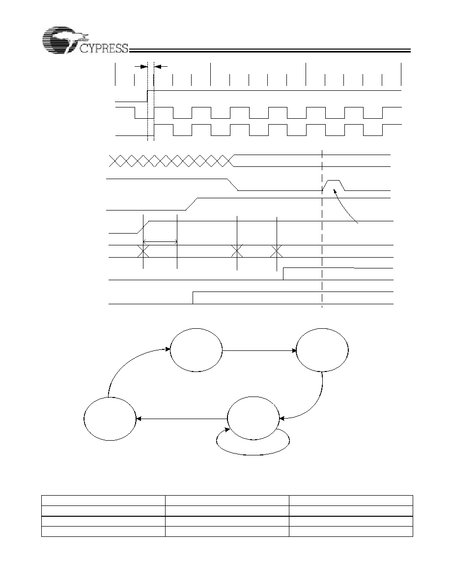
PD# (Power-down) Clarification
The PD# (Power-down) pin is used to shut off ALL clocks prior
to shutting off power to the device. PD# is an asynchronous
active LOW input. This signal is synchronized internally to the
device powering down the clock synthesizer. PD# is an
asynchronous function for powering up the system. When PD#
is low, all clocks are driven to a LOW value and held there and
the VCO and PLLs are also powered down. All clocks are shut
down in a synchronous manner so has not to cause glitches
while transitioning to the low `stopped' state.
PD#≠Assertion
When PD# is sampled LOW by two consecutive rising edges
of the CPUC clock, then on the next HIGH-to-LOW transition
of PCIF, the PCIF clock is stopped LOW. On the next
HIGH-to-LOW transition of 66Buff, the 66Buff clock is stopped
LOW. From this time, each clock will stop LOW on its next
HIGH-to-LOW transition, except the CPUT clock. The CPU
clocks are held with the CPUT clock pin driven HIGH with a
value of 2 x Iref, and CPUC undriven. After the last clock has
stopped, the rest of the generator will be shut down.
Table 4. Spread Spectrum
SS2
SS1
SS0
Spread Mode
Spread%
0
0
0
Down
+0.00, ≠0.25
0
0
1
Down
+0.00, ≠0.50
0
1
0
Down
+0.00, ≠0.75
0
1
1
Down
+0.00, ≠1.00
1
0
0
Center
+0.13, ≠0.13
1
0
1
Center
+0.25, ≠0.25
1
1
0
Center
+0.37, ≠0.37
1
1
1
Center
+0.50, ≠1.50
66Buff
PCIF
PW RDW N#
CPU 133MHz
CPU# 133MHz
3V66
66In
REF 14.318MHz
USB 48MHz
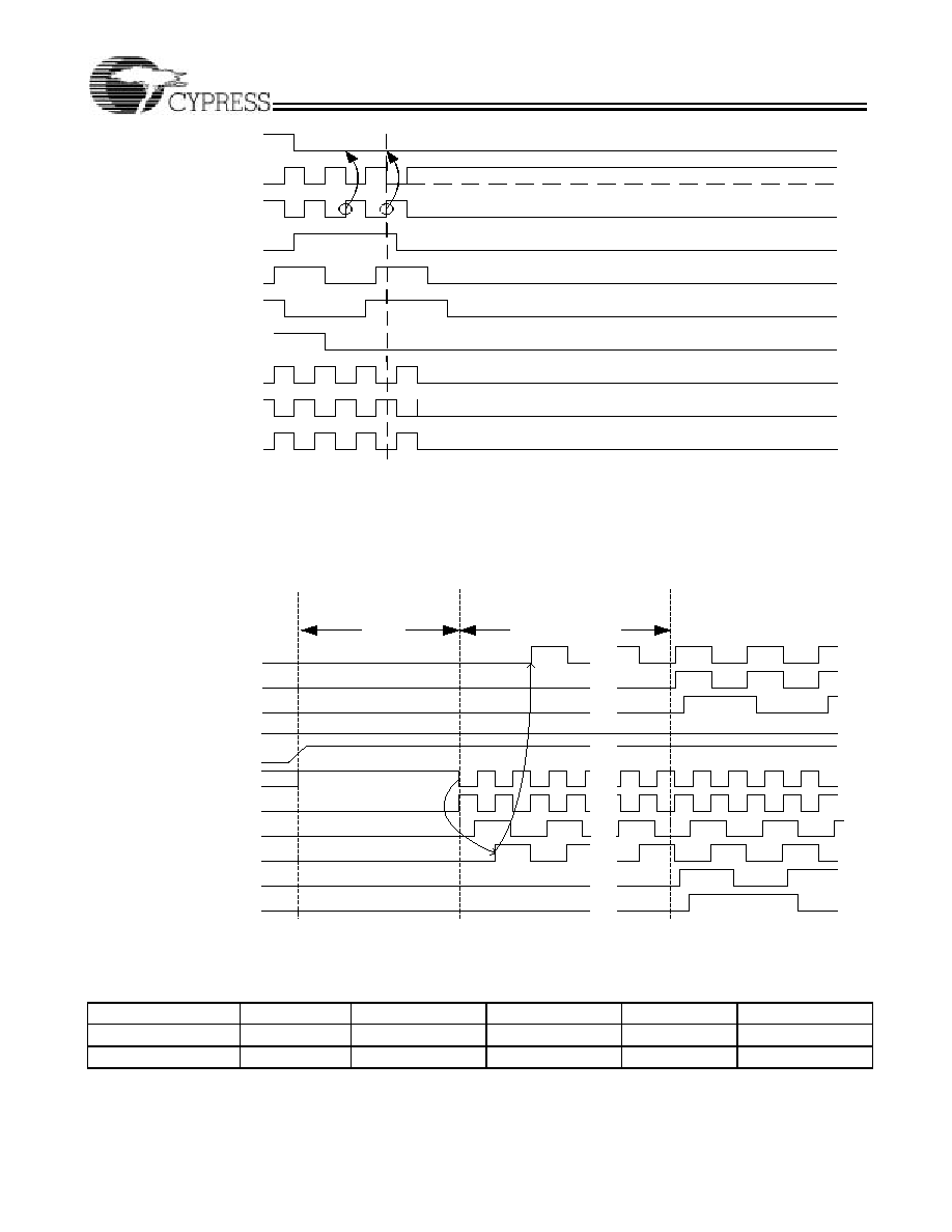
Figure 1. Power-down Assertion Timing Waveforms≠Buffered Mode
CY28346-2
Document #: 38-07509 Rev. *A
Page 8 of 20
PD# Deassertion
The power-up latency between PD# rising to a valid logic `1'
level and the starting of all clocks is less than 3.0 ms.
P C I 3 3 M H z
P W R D W N #
C P U T 1 3 3 M H z
C P U C 1 3 3 M H z
R E F 1 4 .3 1 8 M H z
U S B 4 8 M H z
S D R A M 1 3 3 M H z
D D R T 1 3 3 M H z
D D R C 1 3 3 M H z
A G P 6 6 M H z
Figure 2. Power-down Assertion Timing Waveforms≠Unbuffered Mode
CPU 133MHz
3V66
CPU# 133MHz
REF 14.318MHz
USB 48MHz
PCIF / APIC
33MHz
66In
66Buff
PWRDWN#
66Buff1 / GMCH
400uS max
<1.8mS
PCI 33MHz
30uS min
Figure 3. Power-down Deassertion Timing Waveforms
Table 5. PD# Functionality
PD#
DRCG
66CLK (0:2)
PCIF/PCI
PCI
USB/DOT
1
66M
66Input
66Input/2
66Input/2
48M
0 Low
Low
Low
Low
Low
CY28346-2
Document #: 38-07509 Rev. *A
Page 9 of 20
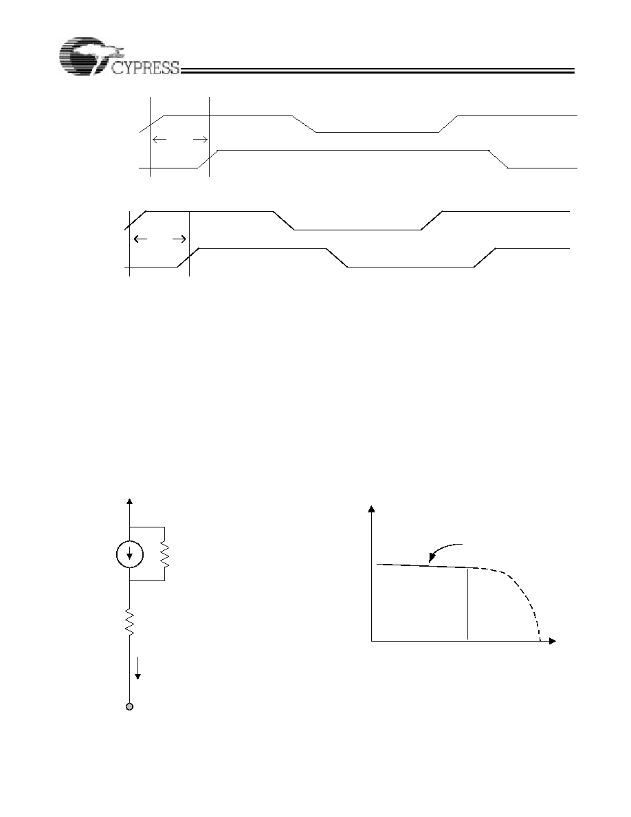
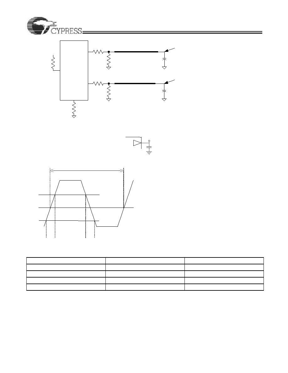
CPU_STP# Clarification
The CPU_STP# signal is an active LOW input used for
synchronous stopping and starting the CPU output clocks
while the rest of the clock generator continues to function.
CPU_STP# Assertion
When CPU_STP# pin is asserted, all CPUT/C outputs that are
set with the SMBus configuration to be stoppable via assertion
of CPU_STP# will be stopped after being sampled by two
falling CPUT/C clock edges. The final state of the stopped
CPU signals is CPUT = HIGH and CPU0C = LOW. There is no
change to the output drive current values during the stopped
state. The CPUT is driven HIGH with a current value equal to
(Mult 0 `select') x (Iref), and the CPUC signal will not be driven.
Due to external pull-down circuitry CPUC will be LOW during
this stopped state.
CPU_STP# Deassertion
The deassertion of the CPU_STP# signal will cause all
CPUT/C outputs that were stopped to resume normal
operation in a synchronous manner. Synchronous manner
meaning that no short or stretched clock pulses will be
produces when the clock resumes. The maximum latency
from the deassertion to active outputs is no more than two
CPUC clock cycles.
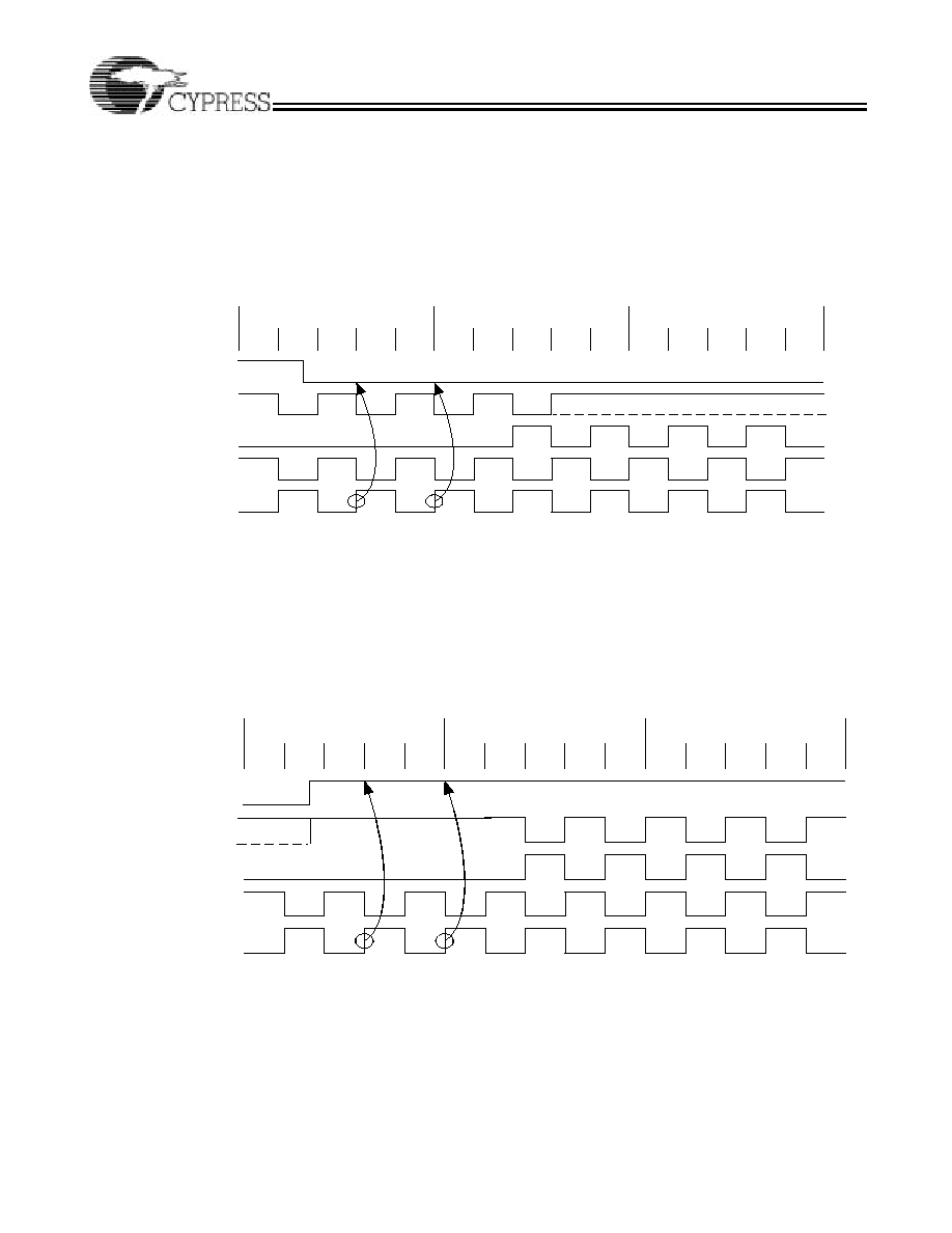
C P U _ S T P #
C P U T
C P U C
C P U T
C P U C
Figure 4. CPU_STP# Assertion Waveforms
CPU_STP#
CPUT
CPUC
CPUT
CPUC
Figure 5. CPU_STP# Deassertion Waveforms
CY28346-2
Document #: 38-07509 Rev. *A
Page 10 of 20
Three-state Control of CPU Clocks Clarification
During CPU_STP# and PD# modes, CPU clock outputs may
be set to driven or undriven (three-state) by setting the corre-
sponding SMBus entry in Bit6 of Byte0 and Bit6 of Byte1.
PCI_STP# Assertion
The PCI_STP# signal is an active LOW input used for
synchronous stopping and starting the PCI outputs while the
rest of the clock generator continues to function. The set-up
time for capturing PCI_STP# going LOW is 10 ns (t
setup
). (See
Figure 2.) The PCIF (0:2) clocks will not be affected by this pin
if their control bits in the SMBus register are set to allow them
to be free running.
PCI_STP# Deassertion
The deassertion of the PCI_STP# signal will cause all PCI and
stoppable PCIF clocks to resume running in a synchronous
manner within two PCI clock periods after PCI_STP# transi-
tions to a high level.
Note that the PCI STOP function is controlled by two inputs.
One is the device PCI_STP# pin number 34 and the other is
SMBus byte 0 bit 3. These two inputs to the function are
logically ANDed. If either the external pin or the internal
SMBus register bit is set low then the stoppable PCI clocks will
be stopped in a logic low state. Reading SMBus Byte 0 Bit 3
will return a 0 value if either of these control bits are set LOW
thereby indicating the devices stoppable PCI clocks are not
running.
Table 6. Cypress Clock Power Management Truth Table
B0b6
B1b6
PD#
CPU_STP#
Stoppable
CPUT
Stoppable
CPUC
Non-Stop CPUT
Non-Stop CPUC
0
0
1
1
Running
Running
Running
Running
0
0
1
0
Iref x6
Iref x6
Running
Running
0
0
0
1
Iref x2
Low
Iref x2
Low
0
0
0
0
Iref x2
Low
Iref x2
Low
0
1
1
1
Running
Running
Running
Running
0
1
1
0
Hi Z
Hi Z
Running
Running
0
1
0
1
Hi Z
Hi Z
Hi Z
Hi Z
0
1
0
0
Hi Z
Hi Z
Hi Z
Hi Z
1
0
1
1
Running
Running
Running
Running
1
0
1
0
Iref x6
Iref x6
Running
Running
1
0
0
1
Hi Z
Hi Z
Hi Z
Hi Z
1
0
0
0
Hi Z
Hi Z
Hi Z
Hi Z
1
1
1
1
Running
Running
Running
Running
1
1
1
0
Hi Z
Hi Z
Running
Running
1
1
0
1
Hi Z
Hi Z
Hi Z
Hi Z
1
1
0
0
Hi Z
Hi Z
Hi Z
Hi Z
P C I_S T P #
P C IF 33M
P C I 33M
setup
t
Figure 6. PCI_STP# Assertion Waveforms
CY28346-2
Document #: 38-07509 Rev. *A
Page 11 of 20
PC I_STP #
PC IF
PC I
setup
t
Figure 7. PCI_STP# Deassertion Waveforms
Figure 8. VTT_PWRGD# Timing Diagram
VID
SEL
VTT_PWRGD#
PWRGD
VDD Clock Gen
Clock State
Clock Outputs
Clock VCO
0.2-0.3mS
Delay
State 0
State 2
State 3
Wait for
VTT_PWRGD#
Sample Sels
Off
Off
On
On
State 1
Device is not affected,
VTT_PWRGD# is ignored.
VTT_PWRGD# = Low
Delay
>0.25mS
S1
Power Off
S0
VDDA = 2.0V
Sample
Inputs straps
S2
Normal
Operation
Wait for <1.8ms
Enable Outputs
S3
VTT_PWRGD# = toggle
VDD3.3= off
Figure 9. Clock Generator Power-up/Run State Program
Table 7. Host Clock (HCSL) Buffer Characteristics
Characteristic
Minimum
Maximum
Ro
3000 Ohms (recommended)
N/A
Ros
Vout
N/A
1.2V

CY28346-2
Document #: 38-07509 Rev. *A
Page 12 of 20
Iout is selectable depending on implementation. The param-
eters above apply to all configurations. Vout is the voltage at
the pin of the device.
The various output current configurations are shown in the
host swing select functions table. For all configurations, the
deviation from the expected output current is ±7% as shown in
the current accuracy table.
USB and DOT 48M Phase Relationship
The 48M_USB and 48M_DOT clocks are in phase. It is under-
stood that the difference in edge rate will introduce some in
inherent offset. When 3V66_1/VCH clock is configured for
VCH (48-MHz) operation it is also in phase with the USB and
DOT outputs. See Figure 10.
66IN to 66B Buffered Prop Delay
The 66IN to 66B(0:2) output delay is shown in Figure 11.
The Tpd is the prop delay from the input pin (66IN) to the
output pins (66B[0:2]). The outputs' variation of Tpd is
described in the AC parameters section of this data sheet. The
measurement is taken at 1.5V.
66B to PCI Buffered Clock Skew
Figure 12
shows the difference (skew) between the 3V33(0:5)
outputs when the 66M clocks are connected to 66IN. This
offset is described in the Group Timing Relationship and Toler-
ances section of this data sheet. The measurements were
taken at 1.5V.
3V66 to PCI Unbuffered Clock Skew
Figure 13
shows the timing relationship between 3V66(0:5)
and PCI(0:6) and PCIF when configured to run in the unbuf-
fered mode.
Table 8. CPU Clock Current Select Function
Mult0
Board Target Trace/Term Z
Reference R, Iref ≠ Vdd (3*Rr)
Output Current
Voh @ Z
0
50 Ohms
Rr = 221 1%, Iref = 5.00mA
Ioh = 4*Iref
1.0V @ 50
1
50 Ohms
Rr = 475 1%, Iref = 2.32mA
Ioh = 6*Iref
0.7V @ 50
Table 9. Group Timing Relationship and Tolerances
Description
Offset
Tolerance
Conditions
3V66 to PCI
2.5 ns
±
1.0 ns
3V66 Leads PCI (unbuffered mode)
48M_USB to 48M_DOT Skew
0.0 ns
±
1.0 ns
0 degrees phase shift
66B to PCI offset
2.5 ns
±
1.0 ns
66B leads PCI (buffered mode)
Table 10. Maximum Lumped Capacitive Output Loads
Clock
Max Load
Unit
PCI Clocks
30
pF
3V66 30
pF
66B
30
pF
48M_USB Clock
20
pF
48M_DOT
10
pF
REF Clock
50
pF
48MUSB
48MDOT
Figure 10. 48M_USB and 48M_DOT Phase Relationship
66IN
66B
Tpd
Figure 11. 66IN to 66B(0:2) Output Delay Figure
CY28346-2
Document #: 38-07509 Rev. *A
Page 13 of 20
Buffer Characteristics
Current Mode CPU Clock Buffer Characteristics
The current mode output buffer detail and current reference
circuit details are contained in the previous table of this data
sheet. The following parameters are used to specify output
buffer characteristics:
1. Output impedance of the current mode buffer circuit ≠ Ro
(see Figure 14).
2. Minimum and maximum required voltage operation range
of the circuit ≠ Vop (see Figure 14).
3. Series resistance in the buffer circuit ≠ Ros (see Figure 14).
4. Current accuracy at given configuration into nominal test
load for given configuration.
66B
P CI
PCIF
1.5-
3.5ns
Figure 12. Buffer Mode ≠ 33V66(0:1); 66BUF(0:2) Phase Relationship
PCI
PCIF
Tpci
3V66
Figure 13. Unbuffered Mode ≠ 3V66(0:5) to PCI (0:6) and PCIF(0:2) Phase Relationship
1.2V
0V
Iout
Iout
Ros
Ro
VDD3 (3.3V +/- 5%)
Vout = 1.2V max
Vout
Slope ~ 1/R
0
CY28346-2
Document #: 38-07509 Rev. *A
Page 14 of 20
Absolute Maximum Conditions
Parameter
Description
Condition
Min.
Max.
Unit
V
DD
Core Supply Voltage
≠0.5
4.6
V
V
DD_A
Analog Supply Voltage
≠0.5
4.6
V
V
IN
Input Voltage
Relative to V
SS
≠0.5
V
DD
+ 0.5
VDC
T
S
Temperature, Storage
Non-functional
≠65
150
∞C
T
A
Temperature, Operating Ambient
Functional
0
85
∞C
T
J
Temperature, Junction
Functional
≠
150
∞C
ÿ
JC
Dissipation, Junction to Case
Mil-Spec 883E Method 1012.1
≠
45
∞C/W
ÿ
JA
Dissipation, Junction to Ambient
JEDEC (JESD 51)
≠
15
∞C/W
ESD
HBM
ESD Protection (Human Body Model)
MIL-STD-883, Method 3015
2000
≠
V
Ul-94
Flammability Rating
V≠0 @1/8 in.
≠
10
ppm
MSL
Moisture Sensitivity Level
1
DC Parameters
(V
DD
= V
DDA
= 3.3V ±5%)
Parameter
Description
Conditions
Min.
Typ.
Max.
Unit
Idd3.3V
Dynamic Supply Current
All frequencies at maximum values
[3]
280
mA
Ipd3.3V
Power-down Supply Current
PD# Asserted
Note 4
mA
Cin
Input Pin Capacitance
5
pF
Cout
Output Pin Capacitance
6
pF
Lpin
Pin Inductance
7
nH
Cxtal
Crystal Pin Capacitance
Measured from the Xin or Xout Pin to Ground.
30
36
42
pF
AC Parameters
(V
DD
= V
DDA
= 3.3V ±5%)
Parameter
Description
66 MHz
100 MHz
133 MHz
200 MHz
Unit
Notes
Min.
Max.
Min.
Max.
Min.
Max.
Min.
Max.
Crystal
Tdc
Xin Duty Cycle
47.5
52.5
47.5
52.5
47.5
52.5
47.5
52.5
%
5, 6, 7
Tperiod
Xin Period
69.84
71.0
69.84
71.0
69.84
71.0
69.84
71.0
ns
5, 8, 9, 6
Vhigh
Xin High Voltage
0.7Vdd
Vdd
0.7Vdd
Vdd
0.7Vdd
Vdd
0.7Vdd
Vdd
V
Vlow
Xin Low Voltage
0
0.3Vdd
0
0.3Vdd
0
0.3Vdd
0
0.3Vdd
V
Tr/Tf
Xin Rise and Fall
Times
10.0
10.0
10.0
10.0
ns
10
Tccj
Xin Cycle to Cycle
Jitter
500
500
500
500
ps
8, 11, 6
CPU at 0.7V Timing
Tdc
CPUT and CPUC
Duty Cycle
45
55
45
55
45
55
45
55
%
11, 12, 13
Tperiod
CPUT and CPUC
Period
14.85
15.3
9.85
10.2
7.35
7.65
4.85
5.1
ns
11, 12, 13
Tskew
Any CPU to CPU
Clock Skew
100
100
100
100
ps
8, 11, 12
Notes:
3.
All outputs loaded as per maximum capacitive load table.
4.
Absolute value = ((Programmed CPU Iref) x (2)) + 10 mA.
5.
This parameter is measured as an average over 1-
µ
s duration, with a crystal center frequency of 14.31818 MHz
6.
When Xin is driven from an external clock source.
7.
This is required for the duty cycle on the REF clock out to be as specified. The device will operate reliably with input duty cycles up to 30/70 but the REF clock
duty cycle will not be within data sheet specifications.
8.
All outputs loaded as perTable 10 below.
9.
Probes are placed on the pins and measurements are acquired at 1.5V for 3.3V signals (see test and measurement set-up section of this data sheet).
10. Measured between 0.2Vdd and 0.7Vdd.
11. This measurement is applicable with Spread ON or Spread OFF.
12. Measured at crossing point (Vx) or where subtraction of CLK-CLK# crosses 0 volts Measured from Vol = 0.175V to Voh = 0.525V.
13. Test load is Rta = 33.2 ohms, Rd = 49.9 ohms.
CY28346-2
Document #: 38-07509 Rev. *A
Page 15 of 20
Tccj
CPU Cycle to
Cycle Jitter
150
150
150
150
ps
11, 12, 13
Tr/Tf
CPUT and CPUC
Rise and Fall
Times
175
700
175
700
175
700
175
700
ps
11, 14, 16
Rise/Fall Matching
20%
20%
20%
20%
14, 15, 13
DeltaTr
Rise Time
Variation
125
125
125
125
ps
14, 13
DeltaTf
Fall Time
Variation
125
125
125
125
ps
14, 13
Vcross
Crossing Point
Voltage at 0.7V
Swing
280
430
280
430
280
430
280
430
mV
11, 13
CPU at 1.0V Timing
Tdc
CPUT and CPUC
Duty Cycle
45
55
45
55
45
55
45
55
%
11, 12
Tperiod
CPUT and CPUC
Period
14.85
15.3
9.85
10.2
7.35
7.65
4.85
5.1
nS
11, 12
Tskew
Any CPU to Any
CPU Clock Skew
100
100
100
100
pS
8, 11, 12
Tccj
CPU Cycle to
Cycle Jitter
150
150
150
150
pS
8, 12
Differential
Tr/Tf
CPUT and CPUC
Rise and Fall Times
175
467
175
467
175
467
175
467
ps
11, 16
SE-
DeltaSlew
Absolute Single-
ended Rise/Fall
Waveform
Symmetry
325
325
325
325
ps
17, 18
Vcross
Cross Point at
1.0V swing
510
760
510
760
510
760
510
760
mV
18
3V66
Tdc
3V66 Duty Cycle
45
55
45
55
45
55
45
55
%
8, 9
Tperiod
3V66 Period
15.0
15.3
15.0
15.3
15.0
15.3
15.0
15.3
ns
5, 8, 9
Thigh
3V66 High Time
4.95
4.95
4.95
4.95
ns
19
Tlow
3V66 Low Time
4.55
4.55
4.55
4.55
ns
20
Tr / Tf
3V66 Rise and
Fall Times
0.5
2.0
0.5
2.0
0.5
2.0
0.5
2.0
ns
21
Tskew
Unbuffered
3V66 to 3V66
Clock Skew
500
500
500
500
ps
8, 9
Tskew
Buffered
3V66 to 3V66
Clock Skew
250
250
250
250
ps
8, 9
Tccj
DRCG Cycle to
Cycle Jitter
250
250
250
250
ps
8, 9
14. Measured from Vol = 0.175V to Voh = 0.525V.
15. Determined as a fraction of 2*(Trise ≠ Tfall)/ (Trise + Tfall).
16. Measurement taken from differential waveform, from ≠0.35V to +0.35V.
17. Measurements taken from common mode waveforms, measure rise/fall time from 0.41 to 0.86V. Rise/fall time matching is defined as "the instantaneous
difference between maximum clk rise (fall) and minimum clk# fall (rise) time or minimum clk rise (fall) and maximum clk# fall (rise) time". This parameter is
designed form waveform symmetry.
18. Measured in absolute voltage, i.e. single-ended measurement.
19. THIGH is measured at 2.4V for non host outputs.
20. TLOW is measured at 0.4V for all outputs.
21. Probes are placed on the pins, and measurements are acquired between 0.4V and 2.4V for 3.3V signals (see test and measurement set-up section of this data
sheet).
AC Parameters
(V
DD
= V
DDA
= 3.3V ±5%) (continued)
Parameter
Description
66 MHz
100 MHz
133 MHz
200 MHz
Unit
Notes
Min.
Max.
Min.
Max.
Min.
Max.
Min.
Max.
CY28346-2
Document #: 38-07509 Rev. *A
Page 16 of 20
66B
Tdc
66B(0:2) Duty Cycle
45
55
45
55
45
55
45
55
%
8, 9
Tr / Tf
66B(0:2) Rise and
Fall Times
0.5
2.0
0.5
2.0
0.5
2.0
0.5
2.0
ns
8, 21
Tskew
Any 66B to Any
66B Skew
175
175
175
175
ps
8, 9
Tpd
66IN to 66B(0:2)
Propagation Delay
2.5
4.5
2.5
4.5
2.5
4.5
2.5
4.5
ns
8, 9
Tccj
66B(0:2) Cycle to
Cycle Jitter
100
100
100
100
ps
8, 9, 22
PCI
Tdc
PCIF(0:2) PCI
(0:6) Duty Cycle
45
55
45
55
45
55
45
55
%
8, 9
Tperiod
PCIF(0:2) PCI
(0:6) period
30.0
30.0
30.0
30
nS
5, 8, 9
Thigh
PCIF(0:2) PCI
(0:6) high time
12.0
12.0
12.0
12.0
nS
19
Tlow
PCIF(0:2) PCI
(0:6) low time
12.0
12.0
12.0
12.0
nS
20
Tr/Tf
PCIF(0:2) PCI
(0:6) rise and fall
times
0.5
2.0
0.5
2.0
0.5
2.0
0.5
2.0
nS
21
Tskew
Any PCI clock to
Any PCI clock
Skew
500
500
500
500
pS
8, 9
Tccj
PCIF(0:2) PCI
(0:6) Cycle to
Cycle Jitter
250
250
250
250
ps
8, 9
48M_USB
Tdc
48M_USB Duty
Cycle
45
55
45
55
45
55
45
55
%
8, 9
Tperiod
48M_USB Period 20.8299 20.8333 20.8299 20.8333 20.8299 20.8333 20.8299 20.8333
ns
8, 9
Tr/Tf
48M_USB Rise
and Fall Times
1.0
2.0
1.0
2.0
1.0
2.0
1.0
2.10
ns
8, 21
Tccj
48M_USB Cycle
to Cycle Jitter
350
350
350
350
ps
5, 8, 9
48M_DOT
Tdc
48M_DOT Duty
Cycle
45
55
45
55
45
55
45
55
%
8, 9
Tperiod
48M_DOT Period 20.837
20.837
20.837
20.837
ns
8, 9
Tr/Tf
48M_DOT Rise
and Fall Times
0.5
1.0
0.5
1.0
0.5
1.0
0.5
1.0
ns
8, 9
Tccj
48M_DOT Cycle
to Cycle Jitter
350
350
350
350
ps
8, 9
REF
Tdc
REF Duty Cycle
45
55
45
55
45
55
45
55
%
8, 9
Tperiod
REF Period
69.84
71.0
69.84
71.0
69.84
71.0
69.84
71.0
ns
8, 9
Note:
22. This figure is additive to any jitter already present when the 66IN pin is being used as an input. Otherwise a 500-ps jitter figure is specified.
AC Parameters
(V
DD
= V
DDA
= 3.3V ±5%) (continued)
Parameter
Description
66 MHz
100 MHz
133 MHz
200 MHz
Unit
Notes
Min.
Max.
Min.
Max.
Min.
Max.
Min.
Max.
CY28346-2
Document #: 38-07509 Rev. *A
Page 17 of 20
Test and Measurement Set-up
For Differential CPU Output Signals
The following diagram shows lumped test load configurations
for the differential Host Clock Outputs.
Notes:
23. CPU_STP# and PCI _STP# setup time with respect to any PCIF clock to guarantee that the effected clock will stop or start at the next PCIF clock's rising edge.
24. When Crystal meets minimum 40-ohm device series resistance specification.
Tr / Tf
REF Rise and Fall
Times
1.0
4.0
1.0
4.0
1.0
4.0
1.0
4.0
ns
8, 21
Tccj
REF Cycle to
Cycle Jitter
1000
1000
1000
1000
ps
8, 9
Tpzl/Tpzh
Output Enable
Delay (all outputs)
1.0
10.0
1.0
10.0
1.0
10.0
1.0
10.0
ns
6
Tplz/Tpzh
Output disable
delay (all outputs)
1.0
10.0
1.0
10.0
1.0
10.0
1.0
10.0
ns
6
Tstable
All Clock Stabili-
zation from
Power-up
3
3
3
3
ms
6
Tss
Stopclock Set-up
Time
10.0
10.0
10.0
10.0
ns
23
Tsh
Stopclock Hold
Time
0
0
0
0
ns
23
Tsu
Oscillator Start-up
Time
1.2
1.2
1.2
1.2
ms
24
AC Parameters
(V
DD
= V
DDA
= 3.3V ±5%) (continued)
Parameter
Description
66 MHz
100 MHz
133 MHz
200 MHz
Unit
Notes
Min.
Max.
Min.
Max.
Min.
Max.
Min.
Max.
M ea surem ent P o in t
2p F
C P U T
M U LT S E L
T
P C B
T
P C B
C P U C
220
63.4
63.4
475
33.2
33.2
M e asu rem en t P oint
2 pF
Figure 15. 1.0V Test Load Termination
CY28346-2
Document #: 38-07509 Rev. *A
Page 18 of 20
For Single-Ended Output Signals
CPUT
MULTSEL
T
PCB
T
PCB
CPUC
33
33
Measurement Point
49.9
49.9
2pF
Measurement Point
2pF
221
VDD
Figure 16. 0.7V Test Load Termination
Ordering Information
Part Number
Package Type
Product Flow
CY28346ZC-2
56-pin TSSOP≠Tube
Commercial, 0
∞
to 70
∞
C
CY28346ZC-2T
56-pin TSSOP≠Tape and Reel
Commercial, 0
∞
to 70
∞
C
CY28346ZI-2
56-pin TSSOP≠Tube
Industrial, 0
∞
to 85
∞
C
CY28346ZI-2T
56-pin TSSOP≠Tape and Reel
Industrial, 0
∞
to 85
∞
C
2.4V
0.4V
3.3V
0V
Tr
Tf
1.5V
3.3V signals
tDC
Probe
Output under Test
Load Cap
-
-
Figure 17.
CY28346-2
Document #: 38-07509 Rev. *A
Page 19 of 20
© Cypress Semiconductor Corporation, 2003. The information contained herein is subject to change without notice. Cypress Semiconductor Corporation assumes no responsibility for the use
of any circuitry other than circuitry embodied in a Cypress Semiconductor product. Nor does it convey or imply any license under patent or other rights. Cypress Semiconductor does not authorize
its products for use as critical components in life-support systems where a malfunction or failure may reasonably be expected to result in significant injury to the user. The inclusion of Cypress
Semiconductor products in life-support systems application implies that the manufacturer assumes all risk of such use and in doing so indemnifies Cypress Semiconductor against all charges.
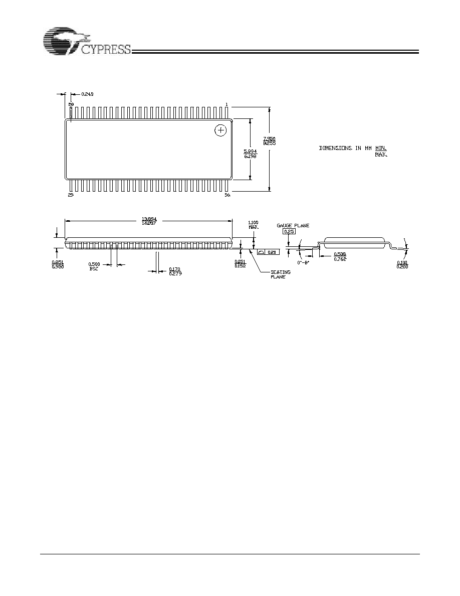
Package Drawings and Dimensions
Intel is a registered trademark of Intel Corporation. Dial-a-Frequency is a registered trademark, and Dial-a-dB is a trademark, of
Cypress Semiconductor. All product and company names mentioned in this document are the trademarks of their respective
holders.
51-85060-*B
56-lead Thin Shrunk Small Outline Package, Type II (6 mm x 14 mm) Z56
CY28346-2
Document #: 38-07509 Rev. *A
Page 20 of 20
Document History Page
Document Title: CY28346-2 Clock Synthesizer with Differential CPU Outputs
Document Number: 38-07509
REV.
ECN NO.
Issue
Date
Orig. of
Change
Description of Change
**
122429
12/11/02
RGL
New Data Sheet
*A
127147
06/10/03
RGL
Corrected the value of T
SU
parameter in the AC parameters table from x to 1.2
Removed "Preliminary" (it is a final data sheet)