 | –≠–ª–µ–∫—Ç—Ä–æ–Ω–Ω—ã–π –∫–æ–º–ø–æ–Ω–µ–Ω—Ç: CY28352OC | –°–∫–∞—á–∞—Ç—å:  PDF PDF  ZIP ZIP |
Differential Clock Buffer/Driver
DDR400- and DDR333 Compliant
CY28352
Cypress Semiconductor Corporation
∑
3901 North First Street
∑
San Jose
,
CA 95134
∑
408-943-2600
Document #: 38-07371 Rev. *B
Revised May 23, 2003
Features
∑ Supports 333-MHz and 400-MHz DDR SDRAM
∑ 60- ≠ 200-MHz operating frequency
∑ Phase-locked loop (PLL) clock distribution for double
data rate synchronous DRAM applications
∑ Distributes one clock input to six differential outputs
∑ External feedback pin FBIN is used to synchronize
output to clock input
∑ Conforms to DDRI specification
∑ Spread Aware
for electromagnetic interference (EMI)
reduction
∑ 28-pin SSOP package
Description
This PLL clock buffer is designed for 2.5-V
DD
and 2.5-AV
DD
operation and differential output levels.
This device is a zero delay buffer that distributes a clock input
CLKIN to six differential pairs of clock outputs (CLKT[0:5],
CLKC[0:5]) and one feedback clock output FBOUT. The clock
outputs are controlled by the input clock CLKIN and the
feedback clock FBIN.
The two-line serial bus can set each output clock pair
(CLKT[0:5], CLKC[0:5]) to the Hi-Z state. When AV
DD
is
grounded, the PLL is turned off and bypassed for test
purposes.
The PLL in this device uses the input clock CLKIN and the
feedback clock FBIN to provide high-performance, low-skew,
low≠jitter output differential clocks.
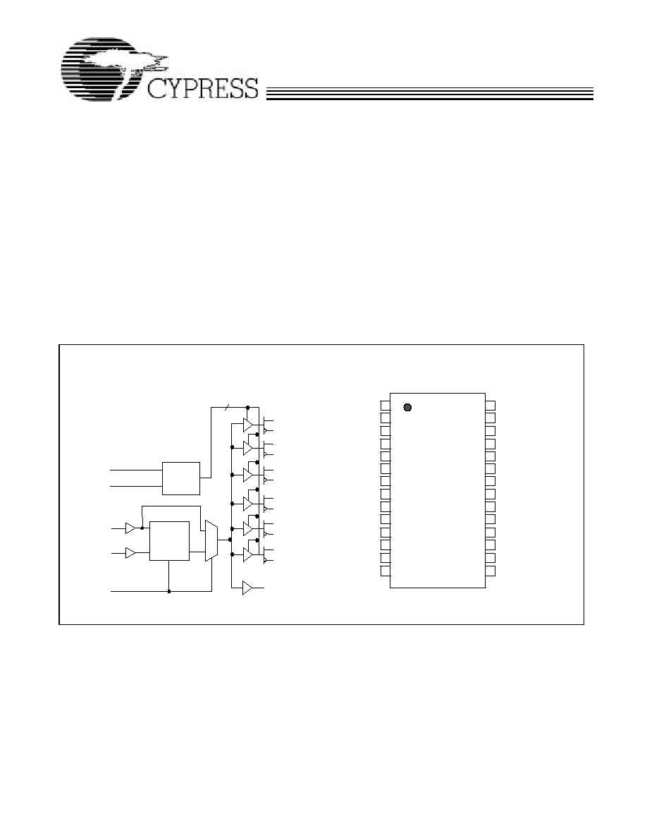
Block Diagram
Pin Configuration
28 pin SSOP
1
2
3
4
5
6
7
8
9
10
11
12
13
14
28
27
26
25
24
23
22
21
20
19
18
17
16
15
GND
CLKT5
NC
FBOUT
CLKT3
CLKC3
GND
NC
FBIN
CLKC5
CLKC4
CLKT4
VDD
SDATA
CLKC0
VDD
CLKIN
AVDD
VDD
CLKT2
CLKC2
AGND
NC
CLKT0
CLKT1
CLKC1
GND
SCLK
C
Y
28352
Serial
Interface
Logic
SDATA
SCLK
CLKT0
FBOUT
CLKC0
CLKT1
CLKC1
CLKT2
CLKC2
CLKC3
CLKT3
CLKC4
CLKT4
CLKC5
CLKT5
PLL
FBIN
CLKIN
AVDD
10
CY28352
Document #: 38-07371 Rev. *B
Page 2 of 8
Zero Delay Buffer
When used as a zero delay buffer the CY28352 will likely be
in a nested clock tree application. For these applications the
CY28352 offers a clock input as a PLL reference. The
CY28352 can then lock onto the reference and translate with
near zero delay to low-skew outputs. For normal operation, the
external feedback input, FBIN, is connected to the feedback
output, FBOUT. By connecting the feedback output to the
feedback input the propagation delay through the device is
eliminated. The PLL works to align the output edge with the
input reference edge thus producing a near zero delay. The
reference frequency affects the static phase offset of the PLL
and thus the relative delay between the inputs and outputs.
When V
DDA
is strapped LOW, the PLL is turned off and
bypassed for test purposes.
Power Management
The individual output enable/disable control of the CY28352
allows the user to implement unique power management
schemes into the design. Outputs are three-stated when
disabled through the two-line interface as individual bits are
set low in Byte0 and Byte1 registers. The feedback output
FBOUT cannot be disabled via two line serial bus. The
enabling and disabling of individual outputs is done in such a
manner as to eliminate the possibility of partial "runt" clocks.
Pin Description
[1]
Pin Number
Pin Name
I/O
Pin Description
Electrical
Characteristics
8
CLKIN
I
Complementary Clock Input.
Input
20
FBIN
I
Feedback Clock Input. Connect to FBOUT for accessing the
PLL.
Input
2,4,13,17,24,
26
CLKT(0:5)
O
Clock Outputs Differential
Outputs
1,5,14,16,25,
27
CLKC(0:5)
O
Clock Outputs
19
FBOUT
O
Feedback Clock Output. Connect to FBIN for normal operation.
A bypass delay capacitor at this output will control Input
Reference/Output Clocks phase relationships.
Output
7
SCLK
I
Serial Clock Input. Clocks data at SDATA into the internal
register.
Data Input for the two line
serial bus
22
SDATA
I/O
Serial Data Input. Input data is clocked to the internal register to
enable/disable individual outputs. This provides flexibility in
power management.
Data Input and Output for
the two line serial bus
3,12,23
VDD
2.5V Power Supply for Logic
2.5V Nominal
10
AVDD
2.5V Power Supply for PLL
2.5V Nominal
6,15,28
GND
Ground
11
AGND
Analog Ground for PLL
9, 18, 21
NC
Not Connected
Function Table
Inputs
Outputs
PLL
VDDA
CLKIN
CLKT(0:5)
[2]
CLKC(0:5)
[2]
FBOUT
GND
L
L
H
L
BYPASSED/OFF
GND
H
H
L
H
BYPASSED/OFF
2.5V
L
L
H
L
On
2.5V
H
H
L
H
On
2.5V
<20 MHz
Hi-Z
Hi-Z
Hi-Z
Off
Notes:
1.
A bypass capacitor (0.1
µ
F) should be placed as close as possible to each positive power pin (< 0.2"). If these bypass capacitors are not close to the pins,
their high-frequency filtering characteristic will be cancelled by the lead inductance of the traces.
2.
Each output pair can be three-stated via the two-line serial interface.
CY28352
Document #: 38-07371 Rev. *B
Page 3 of 8
Serial Control Registers
Following the acknowledge of the Address Byte, two additional
bytes must be sent:
∑ Command Code byte
∑ Byte Count byte.
Byte0: Output Register1 (1 = Enable, 0 = Disable)
Bit
@Pup
Pin#
Description
7
1
2, 1
CLKT0, CLKC0
6
1
4, 5
CLKT1, CLKC1
5
1
≠
Reserved
4
1
≠
Reserved
3
1
13, 14
CLKT2, CLKC2
2
1
26, 27
CLKT5, CLKC5
1
1
≠
Reserved
0
1
24, 25
CLKT4, CLKC4
Byte1: Output Register 2 (1 = Enable, 0 = Disable)
Bit
@Pup
Pin#
Description
7
1
≠
Reserved
6
1
17, 16
CLKT3, CLKC3
5
0
≠
Reserved
4
0
≠
Reserved
3
0
≠
Reserved
2
0
≠
Reserved
1
0
≠
Reserved
0
0
≠
Reserved
Byte2: Test Register 3
Bit
@Pup
Pin#
Description
7
1
≠
0 = PLL leakage test, 1 = disable test
6
1
≠
Reserved
5
0
≠
Reserved
4
0
≠
Reserved
3
0
≠
Reserved
2
0
≠
Reserved
1
0
≠
Reserved
0
0
≠
Reserved

CY28352
Document #: 38-07371 Rev. *B
Page 4 of 8
Maximum Ratings
[3]
Input Voltage Relative to V
SS
:.............................. V
SS
≠ 0.3V
Input Voltage Relative to VDDQ or AV
DD
:............ V
DD
+ 0.3V
Storage Temperature: ................................ ≠65
∞
C to + 150
∞
C
Operating Temperature: .................................... 0
∞
C to +70
∞
C
Maximum Power Supply: ................................................3.5V
This device contains circuitry to protect the inputs against
damage due to high static voltages or electric field; however,
precautions should be taken to avoid application of any
voltage higher than the maximum rated voltages to this circuit.
For proper operation, V
IN
and V
OUT
should be constrained to
the range:
V
SS
< (V
IN
or V
OUT
) < V
DD
.
Unused inputs must always be tied to an appropriate logic
voltage level (either V
SS
or V
DD
).
DC Parameters
V
DDA
= V
DDQ
= 2.5V ± 5%, T
A
= 0
∞
C to +70
∞
C
[4]
Parameter
Description
Condition
Min.
Typ.
Max.
Unit
VIL
Input Low Voltage
SDATA, SCLK
1.0
V
VIH
Input High Voltage
SDATA, SCLK
2.2
V
VIL
Input Voltage Low
CLKIN, FBIN
0.4
V
VIH
Input Voltage High
CLKIN, FBIN
2.1
V
IIN
Input Current
V
IN
= 0V or V
IN
= V
DDQ
, CLKIN,
FBIN
≠10
10
µA
IOL
Output Low Current
V
DDQ
= 2.375V, V
OUT
= 1.2V
26
35
mA
IOH
Output High Current
V
DDQ
= 2.375V, V
OUT
= 1V
≠18
≠32
mA
VOL
Output Low Voltage
V
DDQ
= 2.375V, I
OL
= 12 mA
0.6
V
VOH
Output High Voltage
V
DDQ
= 2.375V, I
OH
= ≠12 mA
1.7
V
VOUT
Output Voltage Swing
[5]
1.1
V
DDQ
≠ 0.4
V
VOC
Output Crossing
Voltage
[6]
(V
DDQ
/2) ≠
0.2
V
DDQ
/2
(V
DDQ
/2) + 0.2
V
IOZ
High-Impedance Output
Current
V
O
= GND or V
O
= V
DDQ
≠10
10
µA
IDDQ
Dynamic Supply
Current
[7]
All V
DDQ
and V
DDI
,
FO = 170 MHz
235
300
mA
IDSTAT
Static Supply Current
1
mA
IDD
PLL Supply Current
V
DDA
only
9
12
mA
Cin
Input Pin Capacitance
4
6
pF
AC Parameters
V
DD
= V
DDQ
= 2.5V ± 5%, T
A
= 0
∞
C to +70
∞
C
[7, 9]
Parameter
Description
Condition
Min.
Typ.
Max.
Unit
fCLK
Operating Clock Frequency
60
200
MHz
tDC
Input Clock Duty Cycle
40
60
%
tlock
Maximum PLL lock Time
100
µ
s
Tr / Tf
Output Clocks Slew Rate
20% to 80% of V
OD
1
2.5
V/ns
tpZL, tpZH
Output Enable Time
[10]
(all outputs)
3
ns
tpLZ, tpHZ
Output Disable Time
[10]
(all outputs)
3
ns
tCCJ
Cycle-to-Cycle Jitter
[12]
f > 66 MHz
≠100
100
ps
tjit(h-per)
Half-period jitter
[12]
f > 66 MHz
≠100
100
ps
Notes:
3.
Multiple Supplies: The voltage on any input or I/O pin cannot exceed the power pin during power-up. Power supply sequencing is NOT required.
4.
Unused inputs must be held HIGH or LOW to prevent them from floating.
5.
For load conditions, see Figure 7.
6.
The value of V
OC
is expected to be |VTR + VCP|/2. In case of each clock directly terminated by a 120
resistor. See Figure 7.
7.
All outputs switching loaded with 16 pF in 60
environment. SeeFigure 7.
8.
Parameters are guaranteed by design and characterization. Not 100% tested in production.
9.
PLL is capable of meeting the specified parameters while supporting SSC synthesizers with modulation frequency between 30 kHz and 33.3 kHz, with a down
spread of ≠0.5%.
10. Refers to transition of non-inverting output.
11.
All differential input and output terminals are terminated with 120
/16 pF as shown in Figure 7.
12. Period Jitter and Half-Period Jitter specifications are separate, and must be met independently of each other.
CY28352
Document #: 38-07371 Rev. *B
Page 5 of 8
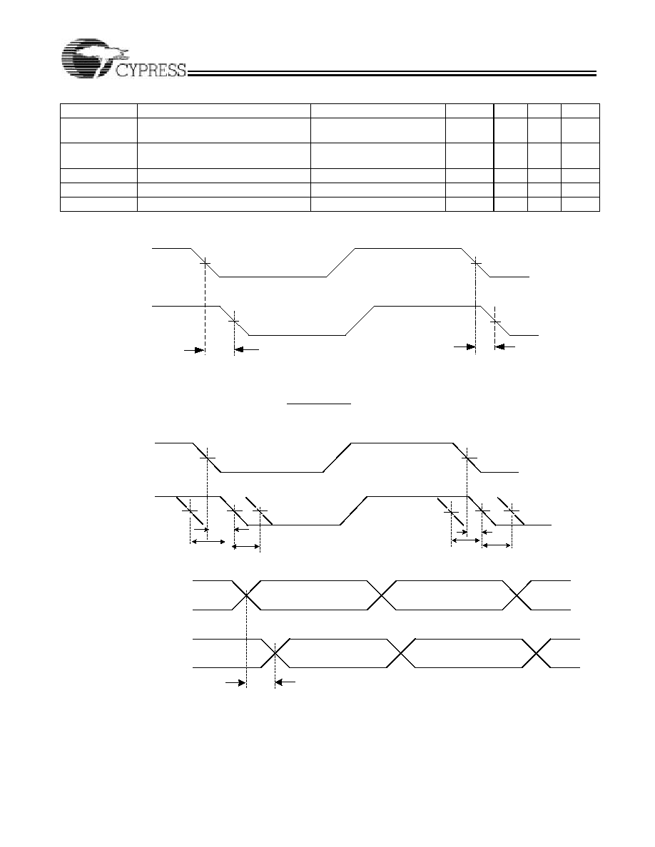
Parameter Measurement Information
tPLH
LOW-to-HIGH Propagation Delay,
CLKIN to CLKT[0:5]
1.5
3.5
6
ns
tPHL
HIGH-to-LOW Propagation Delay,
CLKIN to CLKT[0:5]
1.5
3.5
6
ns
tSKEW
Any Output to Any Output Skew
[11]
100
ps
tPHASE
Phase Error
[11]
≠150
150
ps
tPHASEJ
Phase Error Jitter
f > 66 MHz
≠50
50
ps
AC Parameters
V
DD
= V
DDQ
= 2.5V ± 5%, T
A
= 0
∞
C to +70
∞
C (continued)
[7, 9]
Parameter
Description
Condition
Min.
Typ.
Max.
Unit
t
(
)
n =
n =N
t
(
)
n
(N is large number of samples)
1
t
(
)
n
t
(
)
n+1
CLKIN
FBIN
1.25V
1.25V
1.25V
1.25V
Figure 1. Static Phase Offset
td(
)
td(
)
t(
)
t(
)
td(
)
td(
)
CLKIN
FBIN
1.25V
1.25V
Figure 2. Dynamic Phase Offset
CLKT[0:5], FBOUT
tsk(o)
CLKC[0:5]
CLKT[0:5], FBOUT
CLKC[0:5]
Figure 3. Output Skew