 | –≠–ª–µ–∫—Ç—Ä–æ–Ω–Ω—ã–π –∫–æ–º–ø–æ–Ω–µ–Ω—Ç: CY28357OC | –°–∫–∞—á–∞—Ç—å:  PDF PDF  ZIP ZIP |
PRELIMINARY
200-MHz Differential Clock Buffer/Driver
CY28357
Cypress Semiconductor Corporation
∑
3901 North First Street
∑
San Jose
∑
CA 95134
∑
408-943-2600
Document #: 38-07416 Rev. *A
Revised December 27, 2002
57
Features
∑ Up to 200 MHz operation
∑ Phase-locked loop clock distribution for Double Data
Rate Synchronous DRAM applications
∑ Distributes one clock input to ten differential outputs
∑ External feedback pin (FBIN) is used to synchronize the
outputs to the clock input
∑ Conforms to the DDR1 specification
∑ Spread AwareTM for EMI reduction
∑ 48-pin SSOP package
Description
This PLL clock buffer is designed for 2.5-VDD and 2.5-AVDD
operation and differential outputs levels.
This device is a zero delay buffer that distributes a clock input
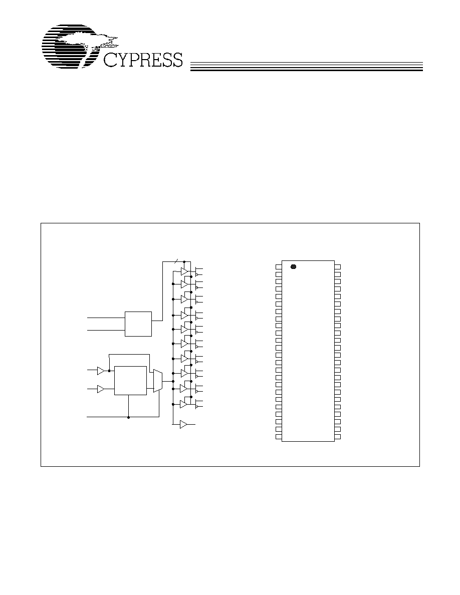
(CLKIN) to ten differential pairs of clock outputs (YT[0:9],
YC[0:9]) and one feedback clock output (FBOUT). The clock
outputs are individually controlled by the serial inputs SCLK
and SDATA.
The two line serial bus can set each output clock pair (YT[0:9],
YC[0:9]) to the Hi-Z state. When AVDD is grounded, the PLL
is turned off and bypassed for the test purposes.
The PLL in this device uses the input clock (CLKIN) and the
feedback clock (FBIN) to provide high-performance, low-skew,
low-jitter output differential clocks.
Block Diagram
Pin Configuration
1
2
3
4
5
6
7
8
9
10
11
12
13
14
15
16
17
18
19
20
21
22
23
24
48
47
46
45
44
43
42
41
40
39
38
37
36
35
34
33
32
31
30
29
28
27
26
25
C
Y
2
8357
NC
YC0
YT0
VDDQ
YT1
YC1
VSS
VSS
YC2
YT2
VDD
SCLK
CLKIN
NC
VDDQ
AVDD
AVSS
VSS
YC3
YT3
VDDQ
YT4
YC4
NC
VSS
YC5
YT5
VDDQ
YT6
YC6
VSS
VSS
YC7
YT7
VDDQ
SDATA
NC
FBIN
VDDQ
FBOUT
NC
VSS
YC8
YT8
VDDQ
YT9
YC9
VSS
YT0
YC0
YT1
YC1
YT2
YC2
YT3
YC3
YT4
YC4
YT5
YC5
YT6
YC6
YT7
YC7
YT8
YC8
YT9
YC9
FBOUT
Serial
Interface
Logic
PLL
FBIN
CLKIN
SDATA
SCLK
AVDD
10
CY28357
PRELIMINARY
Document #: 38-07416 Rev. *A
Page 2 of 12
Note:
1.
A bypass capacitor (0.1
µ
F) should be placed as close as possible to each positive power pin (<0.2"). If these bypass capacitors are not close to the pins their
high frequency filtering characteristic will be cancelled by the lead inductance of the traces.
Pin Description
[1]
Pin
Name
I/O
Description
Electrical Characteristics
13
CLKIN
I
Clock Input.
Input
35
FBIN
I
Feedback Clock Input. Connect to FBOUT for
accessing the PLL.
Input
3, 5, 10, 20, 22
46, 44, 39, 29,27
YT(0:9)
O
Clock Outputs
Differential Outputs
2, 6, 9, 19, 23
47, 43, 40,30,26
YC(0:9)
O
Clock Outputs
33
FBOUT
O
Feedback Clock Output. Connect to FBIN for
normal operation. A bypass delay capacitor at
this output will control Input Reference/Output
Clocks phase relationships.
Output
12
SCLK
I
Serial Clock Input. Clocks data at SDATA into
the internal register.
Data Input for the two line serial bus
37
SDATA
I/O
Serial Data Input. Input data is clocked to the
internal register to enable/disable individual
outputs. This provides flexibility in power
management.
Data Input and Output for the two
line serial bus
11
VDD
2.5V Power Supply for Logic
2.5V Nominal
4, 15, 21, 28, 34,
38, 45
VDDQ
2.5V Power Supply for Output Clock Buffers.
2.5V Nominal
16
AVDD
2.5V Power Supply for PLL
2.5V Nominal
1, 24
NC
No Connect
7, 8, 18, 25, 31, 41,
42, 48
VSS
Common Ground
0.0V Ground
17
AVSS
Analog Ground
0.0V Analog Ground
14,32,36
NC
Not Connected
CY28357
PRELIMINARY
Document #: 38-07416 Rev. *A
Page 3 of 12
Zero Delay Buffer
When used as a zero delay buffer the CY28357 will likely be
in a nested clock tree application. For these applications the
CY28357 offers a clock input as a PLL reference. The
CY28357 then can lock onto the reference and translate with
near zero delay to low-skew outputs. For normal operation, the
external feedback input, FBIN, is connected to the feedback
output, FBOUT. By connecting the feedback output to the
feedback input the propagation delay through the device is
eliminated. The PLL works to align the output edge with the
input reference edge thus producing a near zero delay. The
reference frequency affects the static phase offset of the PLL
and thus the relative delay between the inputs and outputs.
When VDDA is strapped LOW, the PLL is turned off and by-
passed for test purposes.
Power Management
The individual output enable/disable control of the CY28357
allows the user to implement unique power management
schemes into the design. Outputs are three-stated when dis-
abled through the two-line interface as individual bits are set
low in Byte0 and Byte1 registers. The feedback output
(FBOUT) cannot be disabled via two line serial bus. The en-
abling and disabling of individual outputs is done in such a
manner as to eliminate the possibility of partial "runt" clocks.
Note:
2.
Each output pair can be three-stated via the two line serial interface
Function Table
Input
Outputs
PLL
VDDA
CLKIN
YT(0:9)
[2]
YC(0:9)
[2]
FBOUT
GND
L
L
H
L
BYPASSED/OFF
GND
H
H
L
H
BYPASSED/OFF
2.5V
L
L
H
L
On
2.5V
H
H
L
H
On
2.5V
< 20 MHz
Hi-Z
Hi-Z
Hi-Z
Off

CY28357
PRELIMINARY
Document #: 38-07416 Rev. *A
Page 4 of 12
Serial Data Interface
To enhance the flexibility and function of the clock synthesizer,
a two-signal serial interface is provided. Through the Serial
Data Interface, various device functions, such as individual
clock output buffers, can be individually enabled or disabled.
The registers associated with the Serial Data Interface initial-
ize to their default setting upon power-up, and therefore use of
this interface is optional. Clock device register changes are
normally made upon system initialization, if any are required.
The interface can also be used during system operation for
power management functions.
Data Protocol
The clock driver serial protocol accepts block write, and block
read operations from the controller. For block write/read oper-
ation, the bytes must be accessed in sequential order from
lowest to highest byte (most significant bit first) with the ability
to stop after any complete byte has been transferred. The
block write and block read protocol is outlined in Table 1. The
slave receiver address is 11010010 (D2h).
T
Table 1. Block Read and Block Write Protocol
Block Write Protocol
Block Read Protocol
Bit
Description
Bit
Description
1
Start
1
Start
2:8
Slave address ≠ 7 bits
2:8
Slave address ≠ 7 bits
9
Write = 0
9
Write = 0
10
Acknowledge from slave
10
Acknowledge from slave
11:18
Command Code ≠ 8 bits
'00000000' stands for block operation
11:18
Command Code ≠ 8 bits
'00000000' stands for block operation
19
Acknowledge from slave
19
Acknowledge from slave
20:27
Byte Count ≠ 8 bits
20
Repeat start
28
Acknowledge from slave
21:27
Slave address ≠ 7 bits
29:36
Data byte 1 ≠ 8 bits
28
Read = 1
37
Acknowledge from slave
29
Acknowledge from slave
38:45
Data byte 2 ≠ 8 bits
30:37
Byte count from slave ≠ 8 bits
46
Acknowledge from slave
38
Acknowledge
....
......................
39:46
Data byte from slave ≠ 8 bits
....
Data Byte (N≠1) ≠ 8 bits
47
Acknowledge
....
Acknowledge from slave
48:55
Data byte from slave ≠ 8 bits
....
Data Byte N ≠ 8 bits
56
Acknowledge
....
Acknowledge from slave
....
Data bytes from slave/Acknowledge
....
Stop
....
Data byte N from slave ≠ 8 bits
....
Not Acknowledge
....
Stop
CY28357
PRELIMINARY
Document #: 38-07416 Rev. *A
Page 5 of 12
Byte0: Output Register 1 (1 = Enable, 0 = Disable)
Bit
@Pup
Pin#
Description
7
1
3, 2
YT0, YC0
6
1
5, 6
YT1, YC1
5
1
10, 9
YT2, YC2
4
1
20, 19
YT3, YC3
3
1
22, 23
YT4, YC4
2
1
46, 47
YT5, YC5
1
1
44, 43
YT6, YC6
0
1
39, 40
YT7, YC7
Byte1 Output Register 2 (1 = Enable, 0 = Disable)
Bit
@Pup
Pin#
Description
7
1
29, 30
YT8, YC8
6
1
27, 26
YT9, YC9
5
0
Reserved
4
0
Reserved
3
0
Reserved
2
0
Reserved
1
0
Reserved
0
0
Reserved
Byte2 Test Register 3
Bit
@Pup
Pin#
Description
7
1
Reserved
6
1
Reserved
5
1
Reserved
4
1
Reserved
3
1
Reserved
2
1
Reserved
1
1
Reserved
0
1
Reserved

CY28357
PRELIMINARY
Document #: 38-07416 Rev. *A
Page 6 of 12
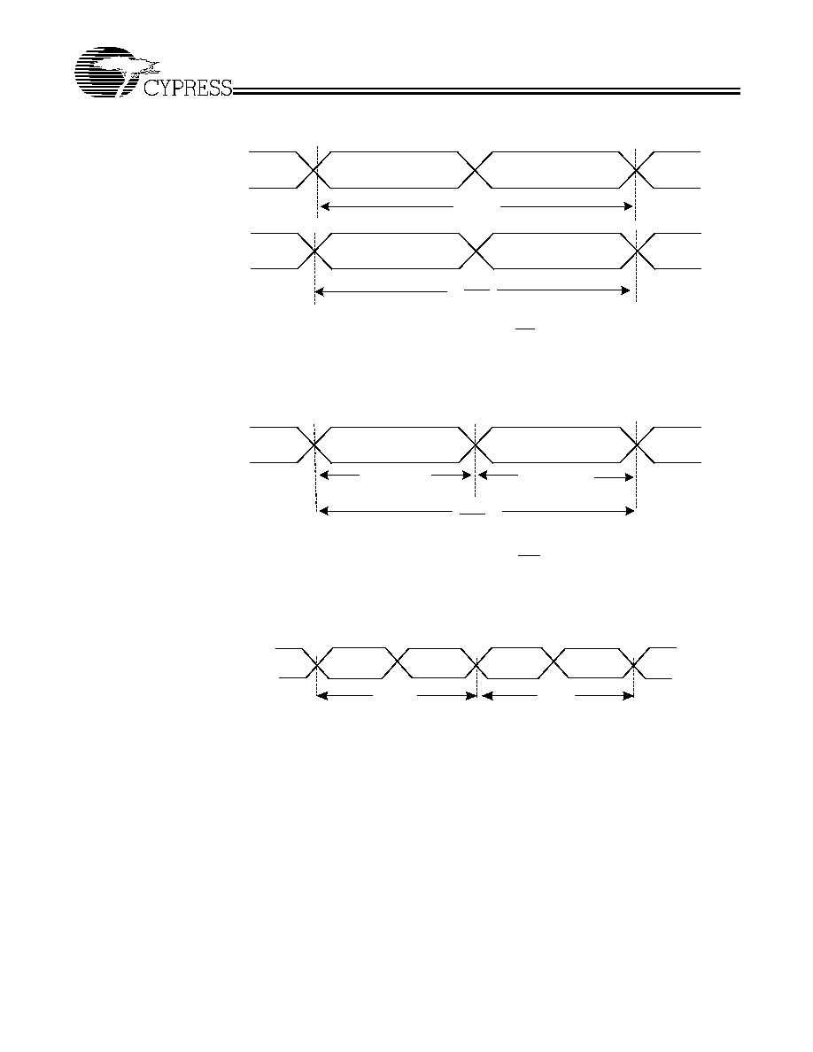
Parameter Measurement Information
t
(
)
n =
n =N
t
(
)
n
(N is large number of samples)
1
t
(
)
n
t
(
)
n+1
CLKIN
FBIN
1.25V
1.25V
1.25V
1.25V
Figure 1. Static Phase Offset
td(
)
td(
)
t (
)
t(
)
td(
)
td(
)
CLKIN
FBIN
1.25V
1.25V
Figure 2. Dynamic Phase Offset
YT[0:9], FBOUT
tsk(o)
YC[0:9]
YT[0:9], FBOUT
YC[0:9]
Figure 3. Output Skew
CY28357
PRELIMINARY
Document #: 38-07416 Rev. *A
Page 7 of 12
t
c(n)
1
f(o)
t
jit(hper)
= t
c(n)
- 1
fo
YT[0:9], FBOUT
YC[0:9]
YT[0:9], FBOUT
YC[0:9]
Figure 4. Period Jitter
1
f(o)
t
(hper_N+1)
t
(hper_n)
t
jit(hper)
= t
hper(n)
- 1
2x fo
YT[0:9], FBOUT
YC[0:9]
Figure 5. Half-Period Jitter
t
jit(cc)
=
c(n)
-
c(n+1)
CLKT[0:5], FBOUT
CLKC[0:5]
t
c(n)
t
c(n)
t
t
Figure 6. Cycle-to-cycle Jitter

CY28357
PRELIMINARY
Document #: 38-07416 Rev. *A
Page 8 of 12
CLKT
T
PCB
T
PCB
CLKC
110
M easurem ent Point
16 pF
M easurem ent Point
16 pF
CLKIN
FBIN
FBO UT
50
50
Figure 7. Differential Signal Using Direct Termination Resistor
CY28357
PRELIMINARY
Document #: 38-07416 Rev. *A
Page 9 of 12
Maximum Ratings
[3]
Input Voltage Relative to V
SS
:...............................V
SS
≠ 0.3V
Input Voltage Relative to V
DDQ
or AV
DD
: ............. V
DD
+ 0.3V
Storage Temperature: ................................ ≠65
∞
C to + 150
∞
C
Operating Temperature: .................................... 0
∞
C to +85
∞
C
Maximum Power Supply: ................................................3.5V
This device contains circuitry to protect the inputs against
damage due to high static voltages or electric field; however,
precautions should be taken to avoid application of any volt-
age higher than the maximum rated voltages to this circuit. For
proper operation, V
in
and V
out
should be constrained to the
range:
V
SS
< (V
in
or V
out
) < V
DD
Unused inputs must always be tied to an appropriate logic volt-
age level (either V
SS
or V
DD
).
Notes:
3.
Multiple Supplies: The voltage on any input or I/O pin cannot exceed the power pin during power-up. Power supply srquencing is NOT required.
4.
unused inputs must be held high or low to prevent them from floating.
5.
For load conditions see Figure 7.
6.
The value of V
OC
is expected to be |VTR + VCP|/2. In case of each clock directly terminated by a 120
resistor. See Figure 7.
7.
All outputs switching loaded with 16 pF in 60
environment. See Figure 7.
DC Parameters
[4]
(V
DD
= V
DDA
= V
DDQ
= V
DDI
= 2.5V ± 5%, T
A
= 0
∞
C to +70
∞
C)
Parameter
Description
Condition
Min.
Typ.
Max.
Unit
V
IL
Input Low Voltage
SDATA, SCLK
1.0
V
V
IH
Input High Voltage
SDATA, SCLK
2.2
V
V
IL
Input Voltage Low
CLKIN, FBIN
0.4
V
V
IH
Input Voltage High
CLKIN, FBIN
2.1
V
I
IN
Input Current
V
IN
= 0V or V
IN
= V
DDQ
, CLKT,
FBIN
≠10
10
µA
I
OL
Output Low Current
V
DDQ
= 2.375V, V
OUT
= 1.2V
26
35
mA
I
OH
Output High Current
V
DDQ
= 2.375V, V
OUT
= 1V
≠18
-32
mA
V
OL
Output Low Voltage
V
DDQ
= 2.375V, I
OL
= 12 mA
0.6
V
V
OH
Output High Voltage
V
DDQ
= 2.375V, I
OH
= ≠12 mA
1.7
V
V
OUT
Output Voltage Swing
[5]
1.1
V
DDQ
≠0.4
V
V
OC
Output Crossing Voltage
[6]
(V
DDQ
/2) ≠
0.2
V
DDQ
/2
(V
DDQ
/2) +
0.2
V
I
OZ
High-Impedance Output
Current
V
O
= G
ND
or V
O
=V
DDQ
≠10
10
µA
I
DDQ
Dynamic Supply Current
[7]
All V
DDQ
and V
DDI
,
F
O
= 200 MHz
235
300
mA
I
DSTAT
Static Supply Current
1
mA
I
DD
PLL Supply Current
V
DDA
only
9
12
mA
C
IN
Input Pin Capacitance
4
6
pF
CY28357
PRELIMINARY
Document #: 38-07416 Rev. *A
Page 10 of 12
Notes:
8.
Parameters are guaranteed by design and characterization. Not 100% tested in production.
9.
PLL is capable of meeting the specified parameters while supporting SSC synthesizers with modulation frequency between 30 kHz and 33.3 kHz with a down
spread of ≠0.5%.
10. All differential input and output terminals are terminated with 120
/16 pF as shown in Figure 7.
11. Period Jitter and Half-Period Jitter specifications are separate specifications that must be met independently of each other.
AC Parameters
[8,9]
(V
DD
= V
DDQ
= 2.5V ±5%, TA = 0∞C to + 70∞C)
Parameter
Description
Condition
Min.
Typ.
Max.
Unit
f
CLK
Operating Clock Frequency
60
200
MHz
t
DC
Input Clock Duty Cycle
40
60
%
t
LOCK
Maximum PLL lock Time
100
µ
s
t
R
/t
F
Output Clocks Slew Rate
20% to 80% of V
OD
1
2.5
V/ns
t
CCJ
Cycle to Cycle Jitter
[11]
f > 66 MHz
≠100
100
ps
tjit(h-per)
Half-period jitter
[11]
f > 66 MHz
≠100
100
ps
t
PLH
Low-to-High Propagation Delay, CLKIN
to YT
1.5
3.5
6
ns
t
PHL
High-to-Low Propagation Delay, CLKIN
to YT
1.5
3.5
6
ns
t
SKEW
Any Output to Any Output Skew
[10]
100
ps
t
PHASE
Phase Error
[10]
≠150
150
ps
t
PHASEJ
Phase Error Jitter
f > 66 MHz
≠50
50
ps
CY28357
PRELIMINARY
Document #: 38-07416 Rev. *A
Page 11 of 12
© Cypress Semiconductor Corporation, 2002. The information contained herein is subject to change without notice. Cypress Semiconductor Corporation assumes no responsibility for the use
of any circuitry other than circuitry embodied in a Cypress Semiconductor product. Nor does it convey or imply any license under patent or other rights. Cypress Semiconductor does not authorize
its products for use as critical components in life-support systems where a malfunction or failure may reasonably be expected to result in significant injury to the user. The inclusion of Cypress
Semiconductor products in life-support systems application implies that the manufacturer assumes all risk of such use and in doing so indemnifies Cypress Semiconductor against all charges..
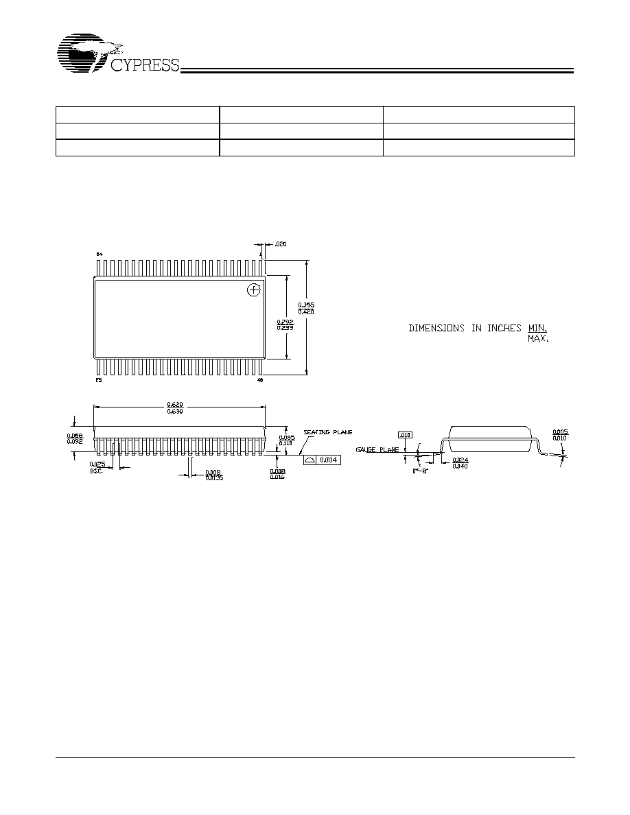
Package Drawing and Dimensions
Spread Aware is a trademark of Cypress Semiconductor Corporation. All product and company names mentioned in this document
may be the trademarks of their respective holders.
Ordering Information
Part Number
Package Type
Product Flow
CY28357OC
48-pin SSOP
Commercial, 0
∞
to 70
∞
C
CY28357OCT
48-pin SSOP - Tape and Reel
Commercial, 0
∞
to 70
∞
C
48-Lead Shrunk Small Outline Package O48
51-85061-*C

CY28357
PRELIMINARY
Document #: 38-07416 Rev. *A
Page 12 of 12
Document History Page
Document Title: CY28357 200-MHz Differential Clock Buffer/Driver
Document #: 38-07416
REV.
ECN NO.
Issue
Date
Orig. of
Change
Description of Change
**
118003
09/11/02
RGL
New Data Sheet
*A
122924
12/27/02
RBI
Add power up requirements to maximum ratings information.