
PRELIMINARY
200-MHz Differential Clock Buffer/Driver
CY28358
Cypress Semiconductor Corporation
∑
3901 North First Street
∑
San Jose
∑
CA 95134
∑
408-943-2600
Document #: 38-07417 Rev. *A
Revised December 14, 2002
58
Features
∑ Up to 200 MHz operation
∑ Phase-locked loop clock distribution for Double Data
Rate Synchronous DRAM applications
∑ Distributes one clock input to six differential outputs
∑ External feedback pin FBIN is used to synchronize the
outputs to the clock input
∑ Conforms to the DDR1 specification
∑ Spread AwareTM for EMI reduction
∑ 28-pin SSOP package
Description
This PLL clock buffer is designed for 2.5 VDD and 2.5 AVDD
operation and differential output levels.
This device is a zero delay buffer that distributes a clock input
CLKIN to six differential pairs of clock outputs (CLKT[0:5],
CLKC[0:5]) and one feedback clock output FBOUT. The clock
outputs are controlled by the input clock CLKIN and the feed-
back clock FBIN.
The two line serial bus can set each output clock pair
(CLKT[0:5], CLKC[0:5]) to the Hi-Z state. When AVDD is
grounded, the PLL is turned off and bypassed for test purpos-
es.
The PLL in this device uses the input clock CLKIN and the
feedback clock FBIN to provide high-performance, low-skew,
low≠jitter output differential clocks.
Block Diagram
Pin Configuration
28 pin SSOP
1
2
3
4
5
6
7
8
9
10
11
12
13
14
28
27
26
25
24
23
22
21
20
19
18
17
16
15
GND
CLKT5
NC
FBOUT
CLKT3
CLKC3
GND
NC
FBIN
CLKC5
CLKC4
CLKT4
VDD
SDATA
CLKC0
VDD
CLKIN
AVDD
VDD
CLKT2
CLKC2
AGND
NC
CLKT0
CLKT1
CLKC1
GND
SCLK
C
Y
28358
Serial
Interface
Logic
SDATA
SCLK
CLKT0
FBOUT
CLKC0
CLKT1
CLKC1
CLKT2
CLKC2
CLKC3
CLKT3
CLKC4
CLKT4
CLKC5
CLKT5
PLL
FBIN
CLKIN
AVDD
10
CY28358
PRELIMINARY
Document #: 38-07417 Rev. *A
Page 2 of 11
Zero Delay Buffer
When used as a zero delay buffer the CY28358 will likely be
in a nested clock tree application. For these applications the
CY28358 offers a clock input as a PLL reference. The
CY28358 then can lock onto the reference and translate with
near zero delay to low-skew outputs. For normal operation, the
external feedback input, FBIN, is connected to the feedback
output, FBOUT. By connecting the feedback output to the
feedback input the propagation delay through the device is
eliminated. The PLL works to align the output edge with the
input reference edge thus producing a near zero delay. The
reference frequency affects the static phase offset of the PLL
and thus the relative delay between the inputs and outputs.
When VDDA is strapped LOW, the PLL is turned off and by-
passed for test purposes.
Power Management
The individual output enable/disable control of the CY28358
allows the user to implement unique power management
schemes into the design. Outputs are three-stated when dis-
abled through the two-line interface as individual bits are set
low in Byte0 and Byte1 registers. The feedback output FBOUT
cannot be disabled via two line serial bus. The enabling and
disabling of individual outputs is done in such a manner as to
eliminate the possibility of partial "runt" clocks.
Notes:
1.
A bypass capacitor (0.1
µ
F) should be placed as close as possible to each positive power pin (<0.2"). If these bypass capacitors are not close to the pins their
high frequency filtering characteristic will be cancelled by the lead inductance of the traces.
2.
Each output pair can be three-stated via the two line serial interface.
Pin Description
[1]
Pin
Name
I/O
Description
Electrical Characteristics
8
CLKIN
I
Clock Input.
Input
20
FBIN
I
Feedback Clock Input. Connect to FBOUT for
accessing the PLL.
Input
2,4,13,17,24,26
CLKT(0:5)
O
Clock Outputs
Differential Outputs
1,5,14,16,25,27
CLKC(0:5)
O
Clock Outputs
19
FBOUT
O
Feedback Clock Output. Connect to FBIN for
normal operation. A bypass delay capacitor at
this output will control Input Reference/Output
Clocks phase relationships.
Output
7
SCLK
I
Serial Clock Input. Clocks data at SDATA into
the internal register.
Data Input for the two line serial bus
22
SDATA
I/O
Serial Data Input. Input data is clocked to the
internal register to enable/disable individual
outputs. This provides flexibility in power
management.
Data Input and Output for the two line
serial bus
3,12,23
VDD
2.5V Power Supply for Logic
2.5V Nominal
10
AVDD
2.5V Power Supply for PLL
2.5V Nominal
6,15,28
GND
Ground
11
AGND
Analog Ground for PLL
9, 18, 21
NC
Not Connected
Function Table
Inputs
Outputs
PLL
VDDA
CLKIN
CLKT(0:5)
[2]
CLKC(0:5)
[2]
FBOUT
GND
L
L
H
L
BYPASSED/OFF
GND
H
H
L
H
BYPASSED/OFF
2.5V
L
L
H
L
On
2.5V
H
H
L
H
On
2.5V
< 20 MHz
Hi-Z
Hi-Z
Hi-Z
Off

CY28358
PRELIMINARY
Document #: 38-07417 Rev. *A
Page 3 of 11
Serial Data Interface
To enhance the flexibility and function of the clock synthesizer,
a two-signal serial interface is provided. Through the Serial
Data Interface, various device functions, such as individual
clock output buffers, can be individually enabled or disabled.
The registers associated with the Serial Data Interface initial-
ize to their default setting upon power-up, and therefore use of
this interface is optional. Clock device register changes are
normally made upon system initialization, if any are required.
The interface can also be used during system operation for
power management functions.
Data Protocol
The clock driver serial protocol accepts block write, and block
read operations from the controller. For block write/read oper-
ation, the bytes must be accessed in sequential order from
lowest to highest byte (most significant bit first) with the ability
to stop after any complete byte has been transferred. The
block write and block read protocol is outlined in Table 1. The
slave receiver address is 11010010 (D2h).
T
Table 1. Block Read and Block Write Protocol
Block Write Protocol
Block Read Protocol
Bit
Description
Bit
Description
1
Start
1
Start
2:8
Slave address ≠ 7 bits
2:8
Slave address ≠ 7 bits
9
Write = 0
9
Write = 0
10
Acknowledge from slave
10
Acknowledge from slave
11:18
Command Code ≠ 8 bits
'00000000' stands for block operation
11:18
Command Code ≠ 8 bits
'00000000' stands for block operation
19
Acknowledge from slave
19
Acknowledge from slave
20:27
Byte Count ≠ 8 bits
20
Repeat start
28
Acknowledge from slave
21:27
Slave address ≠ 7 bits
29:36
Data byte 1 ≠ 8 bits
28
Read = 1
37
Acknowledge from slave
29
Acknowledge from slave
38:45
Data byte 2 ≠ 8 bits
30:37
Byte count from slave ≠ 8 bits
46
Acknowledge from slave
38
Acknowledge
....
......................
39:46
Data byte from slave ≠ 8 bits
....
Data Byte (N≠1) ≠ 8 bits
47
Acknowledge
....
Acknowledge from slave
48:55
Data byte from slave ≠ 8 bits
....
Data Byte N ≠ 8 bits
56
Acknowledge
....
Acknowledge from slave
....
Data bytes from slave/Acknowledge
....
Stop
....
Data byte N from slave ≠ 8 bits
....
Not Acknowledge
....
Stop
CY28358
PRELIMINARY
Document #: 38-07417 Rev. *A
Page 4 of 11
Byte0: Output Register1 (1 = Enable, 0 = Disable)
Bit
@Pup
Pin#
Description
7
1
2, 1
CLKT0, CLKC0
6
1
4, 5
CLKT1, CLKC1
5
1
Reserved
4
1
Reserved
3
1
13, 14
CLKT2, CLKC2
2
1
26, 27
CLKT5, CLKC5
1
1
Reserved
0
1
24, 25
CLKT4, CLKC4
Byte1: Output Register 2 (1 = Enable, 0 = Disable)
Bit
@Pup
Pin#
Description
7
1
Reserved
6
1
17, 16
CLKT3, CLKC3
5
0
Reserved
4
0
Reserved
3
0
Reserved
2
0
Reserved
1
0
Reserved
0
0
Reserved
Byte2: Test Register 3
Bit
@Pup
Pin#
Description
7
1
Reserved
6
1
Reserved
5
1
Reserved
4
1
Reserved
3
1
Reserved
2
1
Reserved
1
1
Reserved
0
1
Reserved
CY28358
PRELIMINARY
Document #: 38-07417 Rev. *A
Page 5 of 11
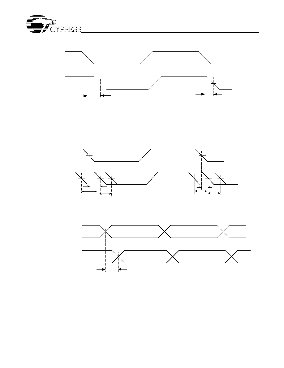
Parameter Measurement Information
t
(
)
n =
n =N
t
(
)
n
(N is large number of samples)
1
t
(
)
n
t
(
)
n+1
CLKIN
FBIN
1.25V
1.25V
1.25V
1.25V
N
Figure 1. Static Phase Offset
td(
)
td(
)
t (
)
t(
)
td(
)
td(
)
CLKIN
FBIN
1.25V
1.25V
Figure 2. Dynamic Phase Offset
CLKT[0:5], FBOUT
tsk(o)
CLKC[0:5]
CLKT[0:5], FBOUT
CLKC[0:5]
Figure 3. Output Skew