PRELIMINARY
273-MHz 6-Output Buffer for DDR400 DIMMS
CY28359
Cypress Semiconductor Corporation
∑
3901 North First Street
∑
San Jose
,
CA 95134
∑
408-943-2600
Document #: 38-07636 Rev. **
Revised February 16, 2004
Features
∑ Dual 1- to 3-output buffer/driver
∑ Supports up to 2 DDR DIMMs
∑ Outputs are individually enabled/disabled
∑ Low-skew outputs (< 100 ps)
∑ Supports 266-MHz, 333-MHz and 400-MHz DDR SDRAM
∑ SMBus Read and Write support
∑ Space-saving 28-pin SSOP package
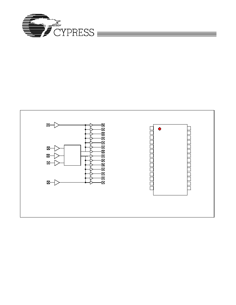
Functional Description
The CY28359 is a 2.5V buffer designed to distribute
high-speed clocks in PC applications. The part has 6 differ-
ential outputs. Designers can configure these outputs to
support up to two DDR DIMMs. The CY28359 can be used in
conjunction with the CY28326 or similar clock synthesizer for
the VIA P4X600 chipset.
The CY28359 also includes an SMBus interface which can
enable or disable each output clock. On power-up, all output
clocks are enabled.
SEL_ADDR
Block Diagram
BUF_INA
SDATA
SCLK
DDRBT2
DDRBC2
Pin Configuration
BUFF_INB
DDRBT0
DDRBC0
DDRBT1
DDRBC1
DDRAT0
DDRAC0
DDRAT1
DDRAC1
DDRAT2
DDRAC2
FB_OUTA
FB_OUTB
SMBus
Decoding
DDRAT2
SDATA
VSS
VDD
DDRAC1
SCLK
DDRAC2
VSS
DDRBT2
DDRBC2
VSS
VDD
FB_OUTB
DDRBT0
VSS
BUF_INA
DDRAT0
DDRAC0
DDRAT1
VSS
FB_OUTA
BUF_INB
DDRBC0
DDRBT1
DDRBC1
VDD
1
2
3
4
5
6
7
8
9
10
11
12
13
14
28
27
26
25
24
23
22
21
20
19
18
17
16
15
28 PIN SSOP
C
Y
2
8
3
5
9
SEL_ADDR
VDD
PRELIMINARY
CY28359
Document #: 38-07636 Rev. **
Page 2 of 8
Serial Data Interface
To enhance the flexibility and function of the clock synthesizer,
a two-signal serial interface is provided. Through the Serial
Data Interface, various device functions, such as individual
clock output buffers, can be individually enabled or disabled.
The registers associated with the Serial Data Interface
initializes to their default setting upon power-up, and therefore
use of this interface is optional. The interface can also be
accessed during power down operation.
Data Protocol
The clock driver serial protocol accepts Byte Write, Byte Read,
Block Write and Block Read operation from any external I
2
C
controller. For Block Write/Read operation, the bytes must be
accessed in sequential order from lowest to highest byte (most
significant bit first) with the ability to stop after any complete
byte has been transferred. For Byte Write and Byte Read
operations, the system controller can access individual
indexed bytes. The offset of the indexed byte is encoded in the
command code, as described in Table 1.
The Block Write and Block Read protocol is outlined in Table 2
while Table 3 outlines the corresponding Byte Write and Byte
Read protocol.The slave receiver address is 11010010 (D2h)
or 11011100 (DCh) depending on state of ADDRSEL.
Pin Description
Pin
Name
PWR
I/O
Description
10
2
BUF_INA,
BUF_INB
VDD2.5
I
Reference input from chipset. 2.5V input.
13,15,20
4,6,24
DDRA[0:2]C
DDRB[0:2]C
VDD2.5
O
Clock outputs. These outputs provide complementary
copies of BUF_INA & BUF_INB, respectively.
12,14,21
3,5,25
DDRA[0:2]T
DDRB[0:2]T
VDD2.5
O
Clock outputs. These outputs provide copies of BUF_INA
& BUF_INB, respectively.
9
1
FB_OUTA
FB_OUTB
VDD2.5
O
Feedback clock for chipset
18
SCLK
VDD2.5
I
SMBus clock input. Has pull-up resistor
19
SDATA
VDD2.5
I/O
SMBus data input. Has pull-up resistor
26
SEL_ADDR
I
Address Select Pin. Has pull-down resistor
7,16,22,28
VDD2.5
2.5V voltage supply
8,11,17,23,27
VSS
Ground
Table 1. Command Code Definition
Bit
Description
7
0 = Block Read or Block Write operation
1 = Byte Read or Byte Write operation
(6:5) 01
(4:0) Byte offset for Byte Read or Byte Write operation. For Block Read or Block Write operations, these bits should be '00000'
PRELIMINARY
CY28359
Document #: 38-07636 Rev. **
Page 3 of 8
Table 2. Block Read and Block Write Protocol
Block Write Protocol
Block Read Protocol
Bit
Description
Bit
Description
1
Start
1
Start
2:8
Slave address ≠ 7 bits
2:8
Slave address ≠ 7 bits
9
Write = 0
9
Write = 0
10
Acknowledge from slave
10
Acknowledge from slave
11:18
Command Code ≠ 8 bits
'00000000' stands for block operation
11:18
Command Code ≠ 8 bits
'00000000' stands for block operation
19
Acknowledge from slave
19
Acknowledge from slave
20:27
Byte Count ≠ 8 bits
20
Repeat start
28
Acknowledge from slave
21:27
Slave address ≠ 7 bits
29:36
Data byte 1 ≠ 8 bits
28
Read = 1
37
Acknowledge from slave
29
Acknowledge from slave
38:45
Data byte 2 ≠ 8 bits
30:37
Byte count from slave ≠ 8 bits
46
Acknowledge from slave
38
Acknowledge from master
....
......................
39:46
Data byte from slave ≠ 8 bits
....
Data Byte (N≠1) ≠ 8 bits
47
Acknowledge from master
....
Acknowledge from slave
48:55
Data byte from slave ≠ 8 bits
....
Data Byte N ≠ 8 bits
56
Acknowledge from master
....
Acknowledge from slave
....
Data byte N from slave ≠ 8 bits
....
Stop
....
Acknowledge from master
....
Stop
Table 3. Byte Read and Byte Write Protocol
Byte Write Protocol
Byte Read Protocol
Bit
Description
Bit
Description
1
Start
1
Start
2:8
Slave address ≠ 7 bits
2:8
Slave address ≠ 7 bits
9
Write = 0
9
Write = 0
10
Acknowledge from slave
10
Acknowledge from slave
11:18
Command Code ≠ 8 bits
'1XXxxxxx' stands for byte operation,bit[6:5] for De-
vice selection bits for multiple device selection,
bits[4:0] of the command code represents the offset
of the byte to be accessed
11:18
Command Code ≠ 8 bits
'1XXxxxxx' stands for byte operation,bit[6:5] for
Device selection bits for multiple device selection,
bits[4:0] of the command code represents the off-
set of the byte to be accessed
19
Acknowledge from slave
19
Acknowledge from slave
20:27
Data byte from master ≠ 8 bits
20
Repeat start
28
Acknowledge from slave
21:27
Slave address ≠ 7 bits
29
Stop
28
Read = 1
29
Acknowledge from slave
30:37
Data byte from slave ≠ 8 bits
38
Acknowledge from master
40
Stop
PRELIMINARY
CY28359
Document #: 38-07636 Rev. **
Page 4 of 8
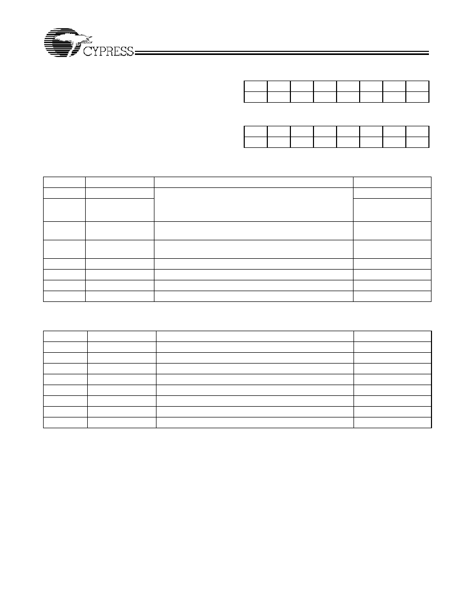
Serial Configuration Map
∑ The Serial bits will be read by the clock driver in the following
order:
Byte 0 - Bits 7, 6, 5, 4, 3, 2, 1, 0
Byte 1 - Bits 7, 6, 5, 4, 3, 2, 1, 0
.
.
Byte N - Bits 7, 6, 5, 4, 3, 2, 1, 0
∑ Reserved and unused bits should be programmed to "0".
SMBus Address for the CY28359 when SEL_ADDR=1:
A6
A5
A4
A3
A2
A1
A0
R/W
1
1
0
1
0
0
1
----
SMBus Address for the CY28359 when SEL_ADDR=0:
A6
A5
A4
A3
A2
A1
A0
R/W
1
1
0
1
1
1
0
----
Byte 22: Outputs Active/Inactive Register (1 = Active, 0 = Three-state), Default = Active
Bit
Pin #
Description
Default
Bit 7
--
Input Threshold Control00: Normal (1.25V)
01: 1.20V
10: 1.15V
11: 1.35V
0
Bit 6
--
0
Bit 5
9
FBOUTA
0 = Enable, 1 = Disable
0
Bit 4
1
FBOUTB
0 = Enable, 1 = Disable
0
Bit 3
Reserved, drive to 0
1
Bit 2
--
Reserved, drive to 0
1
Bit 1
24, 25
DDRBT2, DDRBC2
1
Bit 0
--
Reserved, drive to 0
1
Byte 23: Outputs Active/Inactive Register(1 = Active, 0 = Three-state), Default = Active
Bit
Pin #
Description
Default
Bit 7
5,6
DDRBT1, DDRBC1
1
Bit 6
3,4
DDRBT0, DDRBC0
1
Bit 5
21,20
DDRAT2, DDRAC2
1
Bit 4
--
Reserved, drive to 0
1
Bit 3
14,15
DDRAT1, DDRAC1
1
Bit 2
12,13
DDRAT0, DDRAC0
1
Bit 1
--
Reserved, drive to 0
1
Bit 0
--
Reserved, drive to 0
1
PRELIMINARY
CY28359
Document #: 38-07636 Rev. **
Page 5 of 8
Absolute Maximum Conditions
Supply Voltage to Ground Potential ..................≠0.5 to +4.0V
DC Input Voltage (except BUF_IN) ............ ≠0.5V to V
DD
+0.5
Storage Temperature ..................................≠65∞C to +150∞C
Static Discharge Voltage............................................ >2000V
(per MIL-STD-883, Method 3015)
.
Operating Conditions
Parameter
Description
Min.
Typ.
Max.
Unit
V
DD2.5
Supply Voltage
2.375
≠
2.625
V
T
A
Operating Temperature (Ambient Temperature)
≠40
≠
85
∞C
C
OUT
Output Capacitance
≠
6
≠
pF
C
IN
Input Capacitance
≠
5
≠
pF
Electrical Characteristics
Over the Operating Range
Parameter
Description
Test Conditions
Min.
Typ.
Max.
Unit
V
IL
Input LOW Voltage
For all pins except SMBus
≠
≠
0.8
V
V
IH
Input HIGH Voltage
2.0
≠
≠
V
I
IL
Input LOW Current
V
IN
= 0V
≠
≠
5
µA
I
IH
Input HIGH Current
V
IN
= V
DD
≠
≠
5
µA
I
OH
Output HIGH Current
V
DD
= 2.375V
V
OUT
= 1V
≠18
≠32
≠
mA
I
OL
Output LOW Current
V
DD
= 2.375V
V
OUT
= 1.2V
26
35
≠
mA
V
OL
Output LOW Voltage
I
OL
= 12 mA, V
DD
= 2.375V
≠
≠
0.6
V
V
OH
Output HIGH Voltage
I
OH
= ≠12 mA, V
DD
= 2.375V
1.7
≠
≠
V
I
DD
Supply Current
Unloaded outputs, 273 MHz
≠
≠
250
mA
I
DD
Supply Current
Loaded outputs, 273 MHz
≠
≠
300
mA
V
OUT
Output Voltage Swing
See Test Circuitry (Refer to
Figure 1)
0.7
≠
V
DD
+ 0.6
V
V
OC
Output Crossing Voltage
(V
DD
/2) ≠ 0.2
V
DD
/2
(V
DD
/2) + 0.2
V
IN
DC
Input Clock Duty Cycle
48
52
%
Switching Characteristics
[1]
Parameter
Name
Test Conditions
Min.
Typ.
Max.
Unit
F
O
Operating Frequency
66
≠
273
MHz
T
DC
Duty Cycle = t
2
˜ t
1
Measured at V
DD/
2 for 2.5V outputs. IN
DC
≠ 2%
≠
IN
DC
+ 2%
%
t
3
DDR Rising/Falling Edge Rate
[2]
Measured between 20% to 80% of
output (Refer to Figure 1)
1
≠
3
V/ns
t
4
Output to Output Skew
[2]
All outputs equally loaded
≠
≠
100
ps
Notes:
1. Parameter is guaranteed by design and characterization. Not 100% tested in production
2. All parameters specified with loaded outputs.
PRELIMINARY
CY28359
Document #: 38-07636 Rev. **
Page 6 of 8
Switching Waveforms
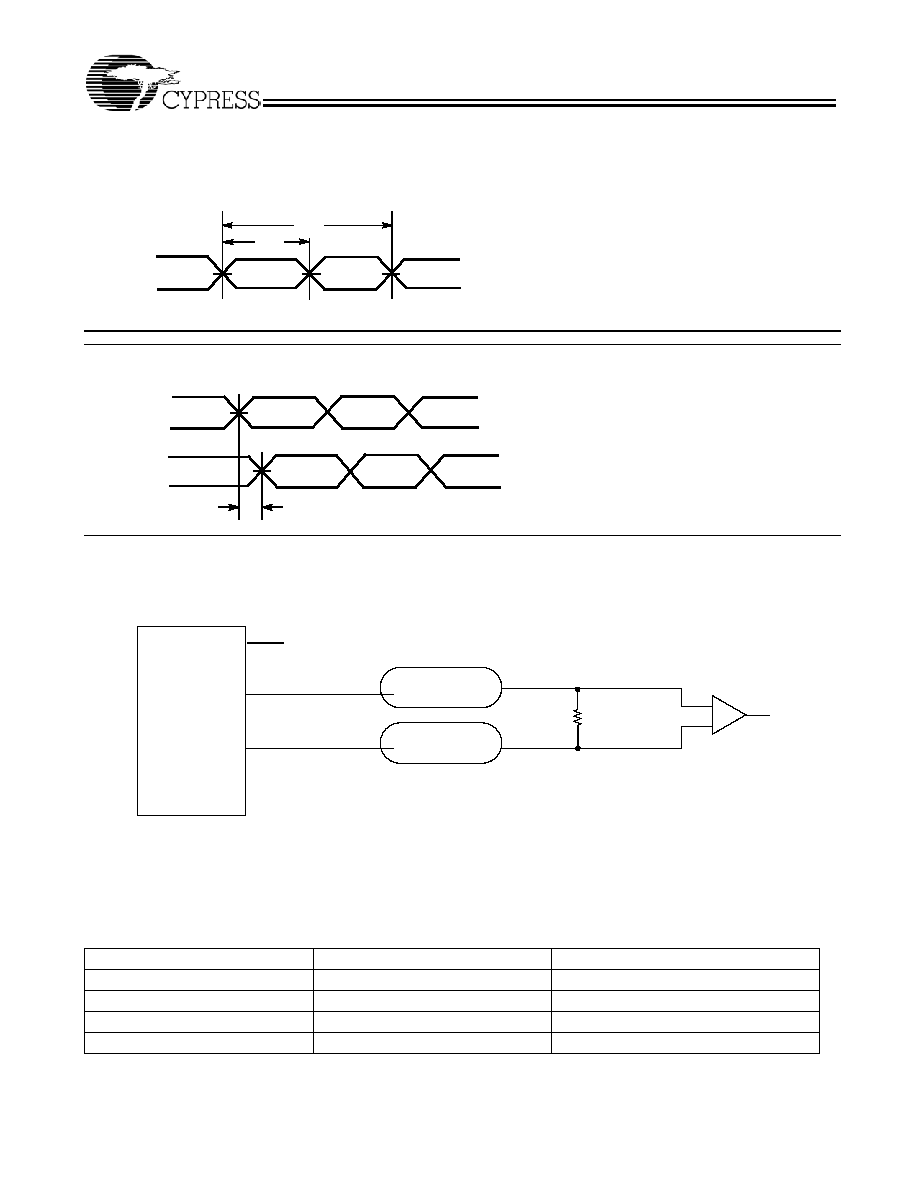
Duty Cycle Timing
t
1
t
2
Output-Output Skew
t
4
OUTPUT
OUTPUT
)
)
R
T
=120
Receiver
60
60
V
CC
V
CC
Device
Under
Test
Figure 1. Differential Signal Using Direct Termination Resistor
Out
Out
VTR
VCP
Figure 1 shows the differential clock directly terminated by a 120
resistor.
Ordering Information
Ordering Code
Package Type
Operating Range
CY28359OC
28-pin SSOP
Commercial, 0∞C to 70 ∞C
CY28359OCT
28-pin SSOP (Tape & Reel)
Commercial, 0∞C to 70 ∞C
CY28359OI
28-pin SSOP
Industrial, ≠40∞C to 85 ∞C
CY28359OIT
28-pin SSOP (Tape & Reel)
Industrial, ≠40∞C to 85 ∞C
PRELIMINARY
CY28359
Document #: 38-07636 Rev. **
Page 7 of 8
© Cypress Semiconductor Corporation, 2004. The information contained herein is subject to change without notice. Cypress Semiconductor Corporation assumes no responsibility for the use
of any circuitry other than circuitry embodied in a Cypress Semiconductor product. Nor does it convey or imply any license under patent or other rights. Cypress Semiconductor does not authorize
its products for use as critical components in life-support systems where a malfunction or failure may reasonably be expected to result in significant injury to the user. The inclusion of Cypress
Semiconductor products in life-support systems application implies that the manufacturer assumes all risk of such use and in doing so indemnifies Cypress Semiconductor against all charges.
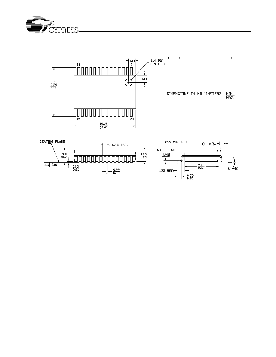
Package Drawing and Dimensions
All product and company names mentioned in this document may be the trademarks of their respective holders.
28-Lead (5.3 mm) Shrunk Small Outline Package O28
51-85079-*C

PRELIMINARY
CY28359
Document #: 38-07636 Rev. **
Page 8 of 8
Document History Page
Document Title: CY28359 273-MHz 6-Output Buffer for DDR400 DIMMS
Document Number: 38-07636
Rev.
ECN No. Issue Date
Orig. of
Change
Description of Change
**
204380
See ECN
RGL
New Data Sheet