 | –≠–ª–µ–∫—Ç—Ä–æ–Ω–Ω—ã–π –∫–æ–º–ø–æ–Ω–µ–Ω—Ç: CY28372 | –°–∫–∞—á–∞—Ç—å:  PDF PDF  ZIP ZIP |
SiS 746 AMD AthlonTM/AMD DuronTM Clock Synthesizer
CY28372
Cypress Semiconductor Corporation
∑
3901 North First Street
∑
San Jose
,
CA 95134
∑
408-943-2600
Document #: 38-07533 Rev. *A
Revised September 20, 2004
Features
∑ Supports AMD Athlon
/Duron CPU
∑ 3.3V and 2.5V power supply
∑ Eight copies of PCI clocks
∑ One 48-MHz USB clock
∑ Two copies of ZCLK clocks
∑ One 48-MHz/24-MHz programmable SIO clock
∑ One differential CPU clock (opendrain)
∑ One singled-ended CPU clock (opendrain)
∑ SMBus support with readback capabilities
∑ Spread Spectrum electromagnetic interference (EMI)
reduction
∑ 48-pin SSOP package
CPU
ZCLK
REF
PCI
AGP
IOAPIC
48M
24_48M
x 2
x 2
x 3
x 8
x 2
x 2
x 1
x 1
~
Block Diagram
Pin Configuration
VDD_REF
CPUT0, CPUC0
XTAL
PLL Ref Freq
XOUT
XIN
VDD_PCI
OSC
SCLK
PLL 1
I2C
Logic
VDD_48
SDATA
VDD_AGP
Divider
Network
VDD_CPU
**FS0:3
2
SSOP-48
REF0:2
AGP0:1
PCIF0:1
PCI0:5
48 MHz
24_48MHz
CPUT1
VDD_REF
**FS0/REF0
**FS1/REF1
REF2
GND_REF
XIN
XOUT
GND_Z
ZCLK0
ZCLK1
VDD_Z
*PCI_STP#
VDD_PCI
**FS2/PCIF0
*FS3/PCIF1
PCI0
PCI1
GND_PCI
VDD_PCI
PCI2
PCI3
PCI4
PCI5
GND_PCI
48
47
46
45
44
43
42
41
40
39
38
37
36
35
34
33
1
2
3
4
5
6
7
8
9
10
11
12
13
14
15
16
17
18
19
20
21
22
23
24
28
27
26
25
32
31
30
29
VDD_APIC
IOAPIC1
IOAPIC0
GND_APIC
CPU_STP#*
CPUT1
VDD_CPU
GND_CPU
CPUT0
CPUC0
VDD_CPU
GNDA
VDDA
SCLK
SDATA
PD#*
GND_AGP
AGP0
AGP1
VDD_AGP
VDD_48
48MHZ
24_48MHZ
GND_48
CY28
372
ZCLK0:1
VDD_Z
APIC0:1
VDD_APIC
PCI_STP#
CPU_STP#
* : Internal Pull-up 150k
** : Internal Pull-down 150k
Fract.
Aligner
PD#
PLL2
2
CY28372
Document #: 38-07533 Rev. *A
Page 2 of 18
Pin Description
Pin #.
Name
Type
Description
6
XIN
I
Crystal Connection or External Reference Frequency Input. This pin has dual
functions. It can be used as an external 14.318-MHz crystal connection or as an
external reference frequency input.
7
XOUT
O
Crystal Connection. Connection for an external 14.318-MHz crystal. If using an
external reference, this pin must be left unconnected.
4
REF2
O
Reference Clock. 14.31818 reference outputs.
2, 3
REF[0:1]/
FS[0:1]
O
Reference Clock. 14.31818 reference outputs.
I
Frequency Select. Sampled upon power-on to determine device operating frequency.
14, 15
PCIF[0:1]/
FS[2:3]
O
Free-running PCI. Independent of PCI_STP#.
I
Frequency Select. Sampled upon power-on to determine device operating frequency.
16, 17, 20,
21, 22, 23
PCI [0:5]
O
PCI Clock.
12
PCI_STP#
I
PCI Stop. Stops all PCI clocks
40
39
CPUT0
CPUC0
O
Differential CPU Outputs.
43
CPUT1
O
"True" Clock of Differential CPU Outputs. For chipset host bus
44
CPU_STP#
I
CPU Stop. Stops all CPU clocks
9, 10
ZCLK[0:1]
O
MuTIOL Clock Outputs.
46, 47
IOAPIC[0:1]
O
IOAPIC. 2.5 V clock outputs
27
48MHz
O
48-MHz Clock. USB clock outputs
26
24_48MHz
O
24-MHz or 48-MHz Clock. Selectable SIO clock outputs. Default output frequency is
24 MHz, but can be configured for 48 MHz through I
2
C.
31, 30
AGP[0:1]
O
AGP Clock.
34
SDATA
I/O
I
2
C Data. 5v tolerant
35
SCLK
I
I
2
C Clock.5v tolerant
33
PD#
I
Power-down Control. Turns off all clock outputs and shuts down device
36
VDDA
PWR
3.3V Analog Power/Ground. Power supply for core logic, PLL circuitry
37
GNDA
PWR
1, 5, 8, 11,
13, 18, 19,
24, 25, 28,
29, 32
VDD_REF,
GND_REF,
GND_Z,
VDD_Z,
VDD_PCI,
GND_PCI,
GND_48,
VDD_48,
VDD_AGP,
GND_AGP
PWR
3.3V Power and Ground. Power supply for respective output buffers.
38, 41, 42
48, 45
VDD_CPU,
GND_CPU,
VDD_APIC,
GND_APIC
PWR
2.5V Power and Ground. Power supply for respective output buffers.

CY28372
Document #: 38-07533 Rev. *A
Page 3 of 18
Serial Data Interface
To enhance the flexibility and function of the clock synthesizer,
a two-signal serial interface is provided. Through the Serial
Data Interface, various device functions, such as individual
clock output buffers, can be individually enabled or disabled.
The registers associated with the Serial Data Interface
initializes to their default setting upon power-up, and therefore
use of this interface is optional. Clock device register changes
are normally made upon system initialization, if any are
required. The interface can also be used during system
operation for power management functions.
Data Protocol
The clock driver serial protocol accepts byte write, byte read,
block write, and block read operations from the controller. For
block write/read operation, the bytes must be accessed in
sequential order from lowest to highest byte (most significant
bit first) with the ability to stop after any complete byte has
been transferred. For byte write and byte read operations, the
system controller can access individually indexed bytes. The
offset of the indexed byte is encoded in the command code,
as described in Table 2.
Table 1. Frequency Selection Table
Input Conditions
Output Frequency
VCO
Freq.
(MHz)
I
2
C Option
(byte 4, bit 2)
FS(3:0)
CPU
(MHz)
ZCLK
(MHz)
AGP
(MHz)
PCI
(MHz)
0
0000
133.3
66.7
66.7
33.3
400.0
0
0001
133.3
66.7
50.0
33.3
400.0
0
0010
133.3
100.0
66.7
33.3
400.0
0
0011
133.3
100.0
50.0
33.3
400.0
0
0100
133.3
133.3
66.7
33.3
400.0
0
0101
133.3
133.3
50.0
33.3
400.0
0
0110
133.3
166.6
66.7
33.3
666.5
0
0111
133.3
166.6
55.5
33.3
666.5
0
(default)
1000
100.0
66.7
66.7
33.3
400.0
0
1001
100.0
66.7
50.0
33.3
400.0
0
1010
100.0
100.0
66.7
33.3
400.0
0
1011
100.0
100.0
50.0
33.3
400.0
0
1100
100.0
133.3
66.7
33.3
400.0
0
1101
100.0
133.3
50.0
33.3
400.0
0
1110
111.0
166.5
66.6
33.3
666.1
0
1111
111.0
166.5
55.5
33.3
666.1
1
0000
114.5
95.4
63.6
31.8
572.5
1
0001
120.0
100.0
66.7
33.3
600.0
1
0010
133.3
83.3
66.7
33.3
666.5
1
0011
133.3
111.1
74.1
33.3
666.5
1
0100
133.3
133.3
83.3
33.3
666.5
1
0101
145.7
116.6
64.8
32.4
582.8
1
0110
150.0
100.0
66.7
33.3
600.0
1
0111
166.6
111.1
66.7
33.3
666.5
1
1000
111.1
133.3
66.7
33.3
666.5
1
1001
137.4
137.4
68.7
34.4
549.6
1
1010
144.9
144.9
64.4
32.2
579.5
1
1011
150.0
150.0
66.7
33.3
600.0
1
1100
155.1
124.1
68.9
34.5
620.3
1
1101
166.6
133.3
66.7
33.3
666.5
1
1110
180.1
135.1
67.6
33.8
540.4
1
1111
200.0
133.3
66.7
33.3
400.0
CY28372
Document #: 38-07533 Rev. *A
Page 4 of 18
The block write and block read protocol is outlined in Table 3
while Table 4 outlines the corresponding byte write and byte
read protocol. The slave receiver address is 11010010 (D2h).
Table 2. Command Code Definition
Bit
Description
7
0 = Block read or block write operation, 1 = Byte
read or byte write operation
(6:0)
Byte offset for byte read or byte write operation.
For block read or block write operations, these bits
should be '0000000'
Table 3. Block Read and Block Write Protocol
Block Write Protocol
Block Read Protocol
Bit
Description
Bit
Description
1
Start
1
Start
2:8
Slave address ≠ 7 bits
2:8
Slave address ≠ 7 bits
9
Write = 0
9
Write = 0
10
Acknowledge from slave
10
Acknowledge from slave
11:18
Command Code ≠ 8 bits
'00000000' stands for block operation
11:18
Command Code ≠ 8 bits
'00000000' stands for block operation
19
Acknowledge from slave
19
Acknowledge from slave
20:27
Byte Count ≠ 8 bits
20
Repeat start
28
Acknowledge from slave
21:27
Slave address ≠ 7 bits
29:36
Data byte 1 ≠ 8 bits
28
Read = 1
37
Acknowledge from slave
29
Acknowledge from slave
38:45
Data byte 2 ≠ 8 bits
30:37
Byte count from slave ≠ 8 bits
46
Acknowledge from slave
38
Acknowledge
....
......................
39:46
Data byte from slave ≠ 8 bits
....
Data Byte (N≠1) ≠8 bits
47
Acknowledge
....
Acknowledge from slave
48:55
Data byte from slave ≠ 8 bits
....
Data Byte N ≠8 bits
56
Acknowledge
....
Acknowledge from slave
....
Data bytes from slave/Acknowledge
....
Stop
....
Data byte N from slave ≠ 8 bits
....
Not Acknowledge
....
Stop
Table 4. Byte Read and Byte Write Protocol
Byte Write Protocol
Byte Read Protocol
Bit
Description
Bit
Description
1
Start
1
Start
2:8
Slave address ≠ 7 bits
2:8
Slave address ≠ 7 bits
9
Write = 0
9
Write = 0
10
Acknowledge from slave
10
Acknowledge from slave
11:18
Command Code ≠ 8 bits
'1xxxxxxx' stands for byte operation, bits[6:0] of the
command code represents the offset of the byte to
be accessed
11:18
Command Code ≠ 8 bits
'1xxxxxxx' stands for byte operation, bits[6:0] of the
command code represents the offset of the byte to
be accessed
19
Acknowledge from slave
19
Acknowledge from slave
20:27
Data byte from master ≠ 8 bits
20
Repeat start
CY28372
Document #: 38-07533 Rev. *A
Page 5 of 18
Device Configuration Map
Data Bytes 0 to 3: Reserved for ZDB Registers
28
Acknowledge from slave
21:27
Slave address ≠ 7 bits
29
Stop
28
Read = 1
29
Acknowledge from slave
30:37
Data byte from slave ≠ 8 bits
38
Not Acknowledge
39
Stop
Table 4. Byte Read and Byte Write Protocol (continued)
Byte Write Protocol
Byte Read Protocol
Bit
Description
Bit
Description
Byte 4
Bit
@Pup
Name
Description
Bit 7
1
Frequency Select Register
(FS3)
[7..4]
CPU
ZCLK AGPPCI
Bit2 = 0
0000
133.3
66.7
66.733.3
0001
133.3
66.7
50.033.3
0010
133.3
100.0
66.733.3
0011
133.3
100.0
50.033.3
0100
133.3
133.3
66.733.3
0101
133.3
133.3
50.033.3
0110
133.3
166.6
66.733.3
0111
133.3
166.6
55.533.3
1000
100.0
66.7
66.733.3
1001
100.0
66.7
50.033.3
1010
100.0
100.0
66.733.3
1011
100.0
100.0
50.033.3
1100
100.0
133.3
66.733.3
1101
100.0
133.3
50.033.3
1110
111.0
166.5
66.633.3
1111
111.0
166.5
55.533.3
Bit2 = 1
0000
114.5
95.4
63.631.8
0001
120.0
100.0
66.733.3
0010
133.3
83.3
66.733.3
0011
133.3
111.1
74.133.3
0100
133.3
133.3
83.333.3
0101
145.7
116.6
64.832.4
0110
150.0
100.0
66.733.3
0111
166.6
111.1
66.733.3
1000
111.1
133.3
66.733.3
1001
137.4
137.4
68.734.4
1010
144.9
144.9
64.432.2
1011
150.0
150.0
66.733.3
1100
155.1
124.1
68.934.5
1101
166.6
133.3
66.733.3
1110
180.1
135.1
67.633.8
1111
200.0
133.3
66.733.3
Bit 6
0
Frequency Select Register
(FS2)
Bit 5
0
Frequency Select Register
(FS1)
Bit 4
0
Frequency Select Register
(FS0)
Bit 3
0
FS_Override
Frequency Selection Source:
0 = Select through hardware strapping, latched inputs
1 = Select through I
2
C
Bit 2
0
Frequency Select Register Most significant bit of I
2
C Frequency Select Register
Bit 1
1
Spread Spectrum Control
0 = Normal, 1 = Spread Spectrum enable
Bit 0
0
Output Disable
0 = Normal, 1 = three-state all outputs
Byte 5
Bit
@Pup
Name
Description
Bit 7
0
Reserved
Reserved
Bit 6
0
Reserved
Reserved
Bit 5
0
Reserved
Reserved
Bit 4
0
Reserved
Reserved
CY28372
Document #: 38-07533 Rev. *A
Page 6 of 18
Bit 3
HW
Latched FS3 input
Latched FS[3:0] inputs. These bits are read-only.
Bit 2
HW
Latched FS2 input
Bit 1
HW
Latched FS1 input
Bit 0
HW
Latched FS0 input
Byte 6
Bit
@Pup
Name
Description
Bit 7
0
Reserved
Reserved
Bit 6
0
Reserved
Reserved
Bit 5
0
PCIF0
PCIF0 functionality when PCI_STP# is LOW
0: Free running, 1: Stop
Bit 4
0
PCIF1
PCIF1 functionality when PCI_STP# is LOW
0: Free running, 1: Stop
Bit 3
1
CPUT0/CPUC0
CPU[T/C]0 functionality when CPU_STP# is LOW
0: Free running, 1: Stop (three-state)
Bit 2
0
CPUT1
CPUT1 functionality when CPU_STP# is LOW
0: Free running, 1: Stop (three-state)
Bit 1
1
CPUT0/CPUC0
CPU[T/C]0 Output Enable/Disable
Bit 0
1
CPUT1
CPUT1 Output Enable/Disable
Byte 7
Bit
@Pup
Name
Description
Bit 7
1
PCIF1
PCIF1 Output Enable/Disable
Bit 6
1
PCIF0
PCIF0 Output Enable/Disable
Bit 5
1
PCI_5
PCI_5 Output Enable/Disable
Bit 4
1
PCI_4
PCI_4 Output Enable/Disable
Bit 3
1
PCI_3
PCI_3 Output Enable/Disable
Bit 2
1
PCI_2
PCI_2 Output Enable/Disable
Bit 1
1
PCI_1
PCI_1 Output Enable/Disable
Bit 0
1
PCI_0
PCI_0 Output Enable/Disable
Byte 8
Bit
@Pup
Name
Pin Description
Bit 7
1
Vendor_ID3
Bit[3] of Cypress Semiconductor's Vendor ID. This bit is read only.
Bit 6
0
Vendor_ID2
Bit[2] of Cypress Semiconductor's Vendor ID. This bit is read only.
Bit 5
0
Vendor _ID1
Bit[1] of Cypress Semiconductor's Vendor ID. This bit is read only.
Bit 4
0
Vendor _ID0
Bit[0] of Cypress Semiconductor's Vendor ID. This bit is read only.
Bit 3
0
Revision_ID3
Revision ID bit[3]
Bit 2
0
Revision_ID2
Revision ID bit[2]
Bit 1
0
Revision_ID1
Revision ID bit[1]
Bit 0
0
Revision_ID0
Revision ID bit[0]
Byte 9
Bit
@Pup
Name
Description
Bit 7
1
PD#
Power-down Enable
Bit 6
0
Reserved
Reserved
Bit 5
1
48MHz
48-MHz Output Control
Byte 5 (continued)
Bit
@Pup
Name
Description

CY28372
Document #: 38-07533 Rev. *A
Page 7 of 18
Bit 4
1
24_48MHz
24_48MHz Output Control
Bit 3
0
24_48MHz
24-MHz or 48-MHz Select
0: 24MHz, 1: 48MHz
Bit 2
0
SS2
Spread Spectrum control bit (0 = down spread, 1 = center spread)
SS[2:0]
Spread Mode
Spread%
000
Down
0,
-0.50 (default)
001
Down
+0.12, -0.62
010
Down
+0.25, -0.75
011
Down
+0.50, -1.00
100
Center
+0.25, -0.25
101
Center
+0.37, -0.37
110
Center
+0.50, -0.50
111
Center
+0.75, -0.75
Bit 1
0
SS1
Bit 0
0
SS0
Byte 10
Bit
@Pup
Name
Description
Bit 7
1
IOAPIC_1
IOAPIC_1 Output Control
Bit 6
1
IOAPIC_0
IOAPIC_0 Output Control
Bit 5
1
REF_1
REF_1 Output Control
Bit 4
1
REF_0
REF_0 Output Control
Bit 3
1
ZCLK_1
ZCLK_1 Output Control
Bit 2
1
ZCLK_0
ZCLK_0 Output Control
Bit 1
1
AGP_1
AGP_1 Output Control
Bit 0
1
AGP_0
AGP_0 Output Control
Byte 11
Bit
@Pup
Name
Description
Bit 7
0
Reserved
Vendor Test Mode (always program to 0)
Bit 6
0
Reserved
Vendor Test Mode (always program to 0)
Bit 5
0
Reserved
Vendor Test Mode (always program to 0)
Bit 4
0
3V66 Fract_Align4
3V66 Frequency Fractional Aligner: These bits determine the 3V66 fixed
frequency. This option does not incorporate spread spectrum.
Fract_Align3V66 (MHz)PCI (MHz)
00000 Off Off(default)
0000166.533.2
0001067.533.7
0001168.534.3
0010069.534.8
0010170.635.3
0011071.635.8
0011172.636.3
0100073.636.8
0100174.737.3
0101075.737.8
0101176.738.4
0110077.738.9
0110178.739.4
0111079.839.9
0111180.840.4
1000081.840.9
1000182.841.4
1001083.941.9
1001184.942.4
1010085.943.0
1010186.943.5
1011088.044.0
1011189.044.5
1100090.045.0
1100191.045.5
1101092.046.0
1101193.146.5
1110094.147.0
1110195.147.6
1111096.148.1
1111197.248.6
Bit 3
0
3V66 Fract_Align3
Bit 2
0
3V66 Fract_Align2
Bit 1
0
3V66 Fract_Align1
Bit 0
0
3V66 Fract_Align0
Byte 9 (continued)
Bit
@Pup
Name
Description
CY28372
Document #: 38-07533 Rev. *A
Page 8 of 18
Byte 12
Bit
@Pup
Name
Description
Bit 7
0
REF_2
REF_2 Output Control (default: off)
Bit 6
0
Reserved
Reserved
Bit 5
0
Reserved
Reserved
Bit 4
0
DARAG2
Dial-a-Ratio
AGP[0:1].
Programming these bits allow modifying the frequency ratio of the
AGP(1:0), PCI(5:0) and PCIF(0:1) clocks relative to the VCO. (the ratio
of AGP to PCI is retained at 2:1)
DARAG[2:0]
VC0/AGP Ratio
000
- (Frequency Selection Default)
001
6
010
8
011
9
100
10
101
12
110
12
111
12
Bit 3
0
DARAG1
Bit 2
0
DARAG0
Bit 1
0
Fixed_PCI_SEL
PCI output frequency select mode
(valid only when Fixed_3V66_SEL = 1)
0 = Use Frequency Selection Table settings
1 = Use Fractional Aligner settings (default)
Bit 0
0
Fixed_3V66_SEL
3V66 and PCI output frequency select mode
0 = Use Frequency Selection Table settings (default)
1 = Use Fractional Aligner settings
Byte 13
Bit
@Pup
Name
Description
Bit 7
0
Reserved
Reserved
Bit 6
0
N6 (MSB)
Dial-a-Frequency
Æ
Control Register N. These bits are for programming
the PLL's internal N register. This access allows the user to modify the
CPU frequency with great accuracy. All other synchronous clocks (clocks
that are generated from the same PLL, such as PCI, remain at their
existing ratios relative to the CPU clock. (should be written together with
Control Register R)
Bit 5
0
N5
Bit 4
0
N4
Bit 3
0
N3
Bit 2
0
N2
Bit 1
0
N1
Bit 0
0
N0 (LSB)
Byte 14
Bit
@Pup
Name
Pin Description
Bit 7
0
Reserved
Reserved
Bit 6
0
R5 (MSB)
Dial-a-Frequency
Control Register R
These bits are for programming the PLL's internal R register. This access
allows the user to modify the CPU frequency with great accuracy. All other
synchronous clocks (clocks that are generated from the same PLL, such
as PCI, remain at their existing ratios relative to the CPU clock.
(should be written together with Control Register N)
Bit 5
0
R4
Bit 4
0
R3
Bit 3
0
R2
Bit 2
0
R1
Bit 1
0
R0 (LSB)
Bit 0
0
R & N Select
R and N register mux selection.
0 = R and N values come from the ROM.
1 = data is loaded from the DAF registers into R and N.
CY28372
Document #: 38-07533 Rev. *A
Page 9 of 18
Dial-A-Frequency Feature
SMBus Dial-a-Frequency feature is available in this device via
Byte13 and Byte14. P is a large value PLL constant that
depends on the frequency selection achieved through the
hardware selectors (FS). P value may be determined from the
following table.
PD# (Power-down) Clarification
The PD# (Power-down) pin is used to shut off ALL clocks prior
to shutting off power to the device. PD# is an asynchronous
active LOW input. This signal is synchronized internally to the
device powering down the clock synthesizer. PD# is an
asynchronous function for powering up the system. When PD#
is low, all clocks are driven to a LOW value and held there and
the VCO and PLLs are also powered down. All clocks are shut
down in a synchronous manner so has not to cause glitches
while transitioning to the low `stopped' state.
PD# ≠ Assertion
FS(4:0)
P
00000, 00001, 00010, 00011, 00100, 00101, 11110
127993333
00110, 00111, 10000, 10001, 10010, 10011, 10100
76796000
01000, 01001, 01010, 01011, 01100, 01101, 10101, 10110, 10111, 11001, 11010, 11011,11100, 11101
95995000
01110, 01111, 11000
63996667
11111
191990000
Table 5. Maximum Lumped Capacitive Output Loads
Clock
Max Load
Unit
PCI, PCIF
20
pF
AGP
30
pF
24_48MHz, 48MHz
20
pF
REF 30
pF
IOAPIC
20
pF
CPUT0/CPUC0
See Figure 7
CPUT1
See Figure 7
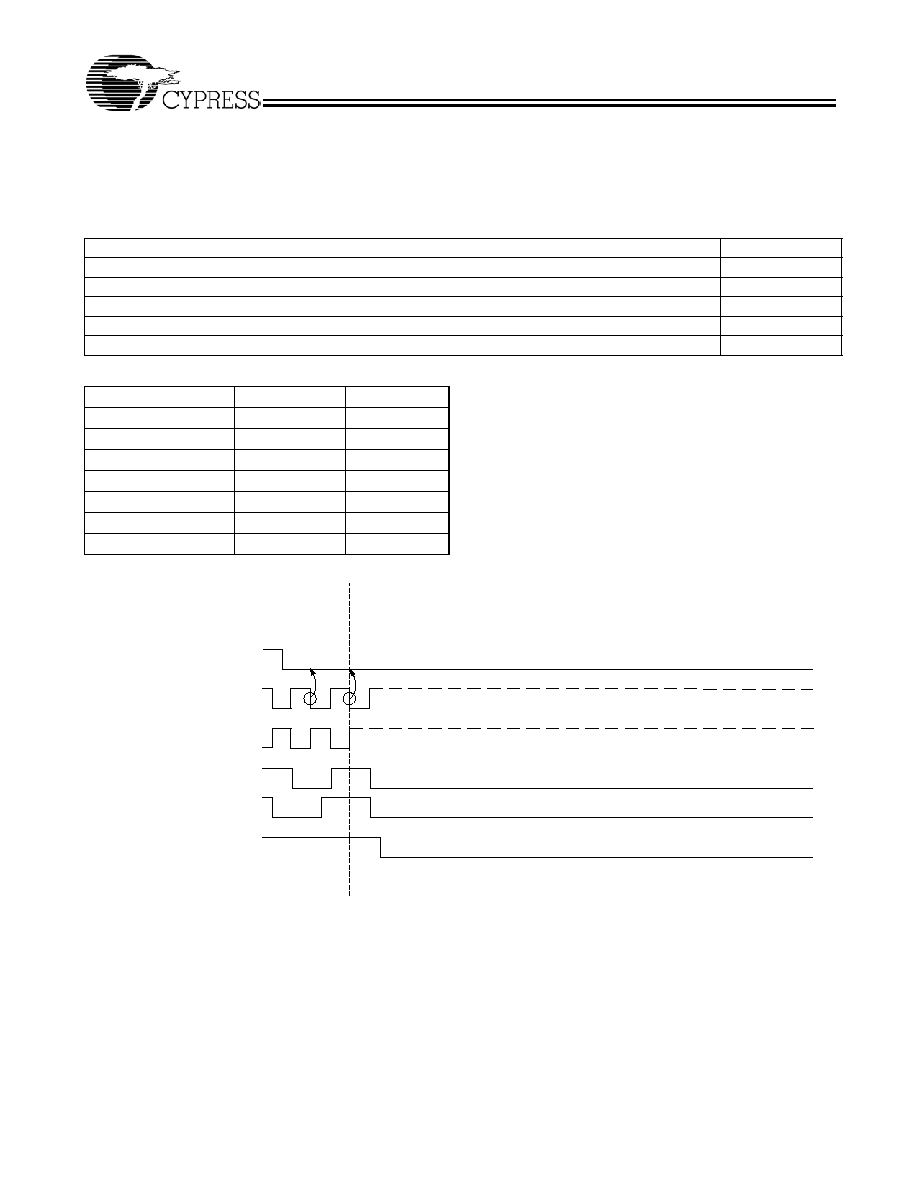
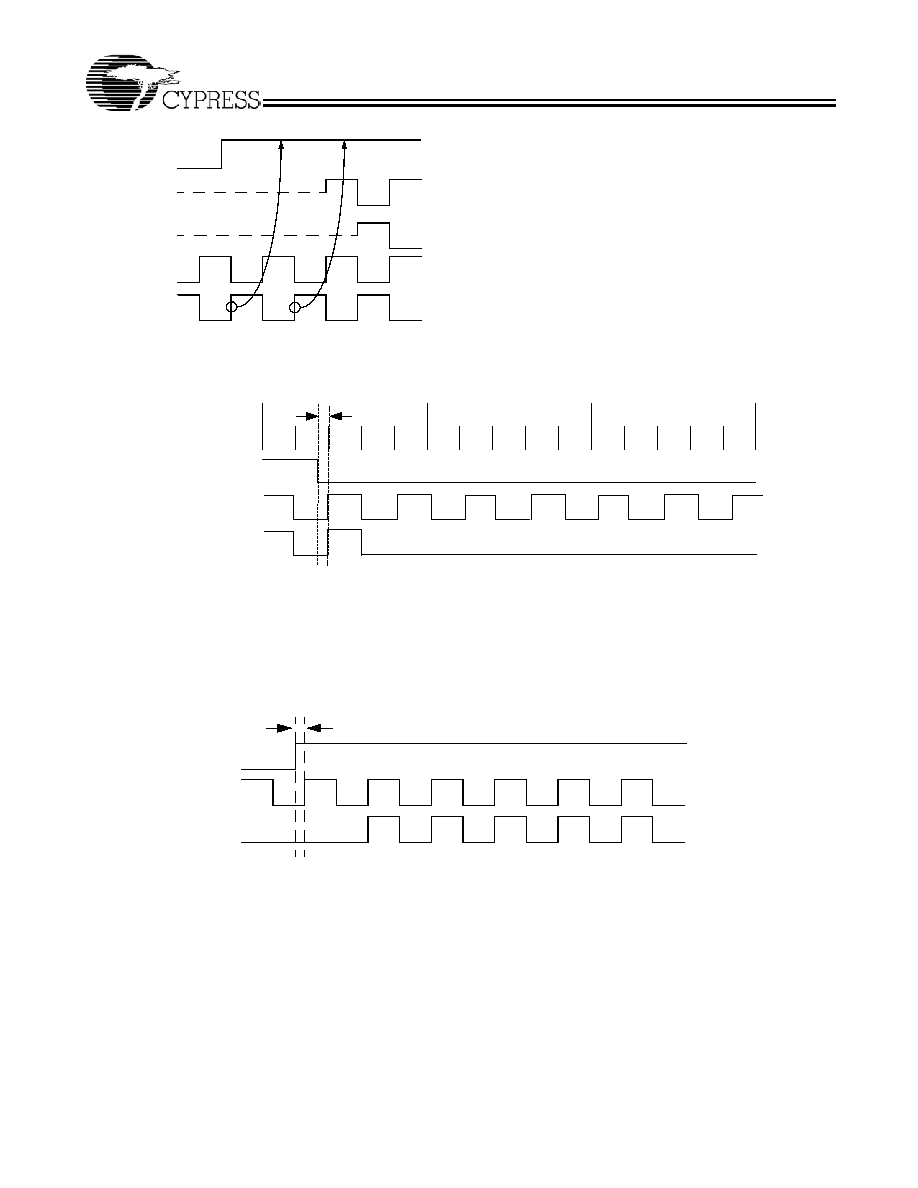
Figure 1. Power-down Assertion Timing Waveforms
PD#
CPUT0
CPUC0
PCI
REF
USB,24_48MHz
Tri-state
Tri-state
CY28372
Document #: 38-07533 Rev. *A
Page 10 of 18
PD# ≠ Deassertion
After the clock chip internal PLL is powered up and locked, all
outputs will be enabled within a few clock cycles of each other,
with the first to last active clock taking no more than two full
PCI clock cycles.
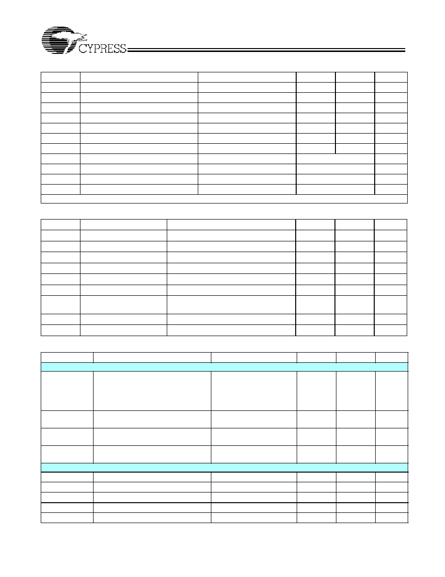
CPU_STP# Clarification
The CPU_STP# signal is an active LOW input used for
synchronous stopping and starting the CPU output clocks
while the rest of the clock generator continues to function.
CPU_STP# ≠ Assertion
When CPU_STP# pin is asserted, all CPUT/C outputs that are
set with the SMBus configuration to be stoppable via assertion
of CPU_STP# will be stopped after being sampled by two
rising CPUC clock edges. The final state of the stopped CPU
signals is CPUT = CPUC = three-state.
CPU_STP# Deassertion
The deassertion of the CPU_STP# signal will cause all
CPUT/C outputs that were stopped to resume normal
operation in a synchronous manner. Synchronous manner
meaning that no short or stretched clock pulses will be
produced when the clock resumes. The maximum latency
from the deassertion to active outputs is no more than two
CPUC clock cycles.
Figure 2. Power Down Deassertion Timing Waveforms
Table 6. PD# Functionality
PD#
CPUT
CPUC
AGP
PCIF/PCI
48MHz
1
Normal
Normal
Normal
Normal
Normal
0
Float
Float
Low
Low
Low
PCI 33MHz
PD#
CPUT
CPUC
3V66
REF 14.318MHz
USB 48MHz
Driven
Driven
1.2 ms
Figure 3. CPU_STP# Assertion Waveform
CPU_STP#
CPUT
CPUC
three-state
three-state
CY28372
Document #: 38-07533 Rev. *A
Page 11 of 18
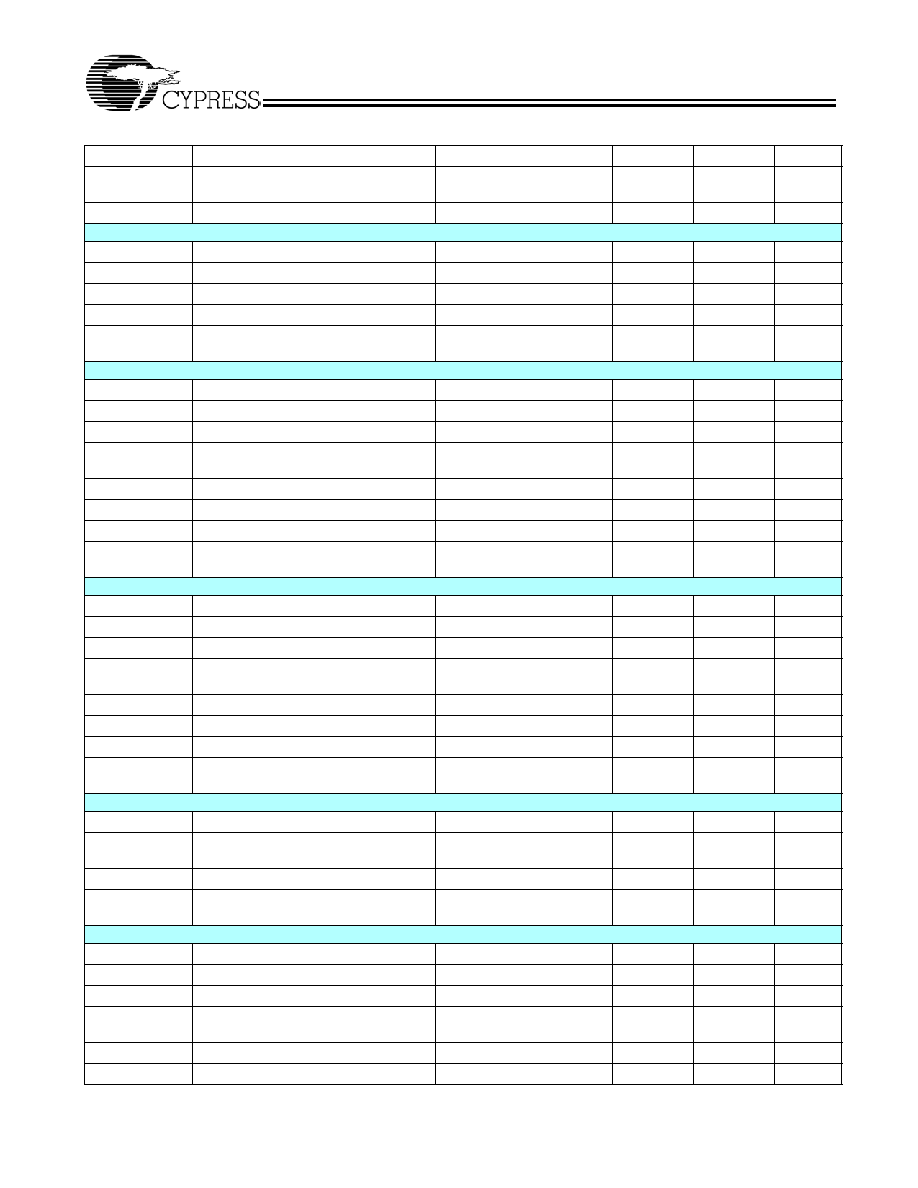
PCI_STP# Assertion
The PCI_STP# signal is an active LOW input used for
synchronous stopping and starting the PCI outputs while the
rest of the clock generator continues to function. The set-up
time for capturing PCI_STP# going LOW is 10 ns (t
setup
). The
PCIF clocks will not be affected by this pin if their control bits
in the SMBus register are set to allow them to be free running.
PCI_STP# - Deassertion
The deassertion of the PCI_STP# signal will cause all PCI and
stoppable PCIF clocks to resume running in a synchronous
manner within two PCI clock periods after PCI_STP# transi-
tions to a high level.
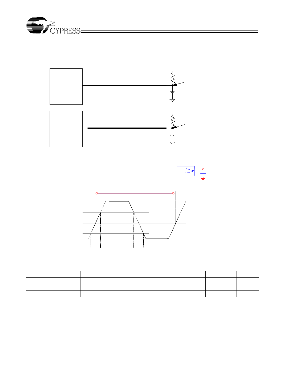
Figure 4. CPU_STP# Deassertion Waveform
CPU_STP#
CPUT
CPUC
three-state
three-state
CPUCint
CPUTint
PCI_STP#
PCIF 33M
PCI 33M
setup
t
Figure 5. PCI_STP# Assertion Waveform
Figure 6. PCI_STP# Deassertion Waveform
t
setup
PCI_STP#
PCIF
PCI
CY28372
Document #: 38-07533 Rev. *A
Page 12 of 18
Absolute Maximum Conditions
Parameter
Description
Condition
Min.
Max.
Unit
V
DD
Core Supply Voltage
≠0.5
4.6
V
V
DDA
Analog Supply Voltage
≠0.5
4.6
V
V
IN
Input Voltage
Relative to V
SS
≠0.5
V
DD
+ 0.5
VDC
T
S
Temperature, Storage
Non-functional
≠65
+150
∞C
T
A
Temperature, Operating Ambient
Functional
0
70
∞C
T
J
Temperature, Junction
Functional
≠
150
∞C
ESD
HBM
ESD Protection (Human Body Model)
MIL-STD-883, Method 3015
2000
≠
V
ÿ
JC
Dissipation, Junction to Case
Mil-Spec 883E Method 1012.1
15
∞C/W
ÿ
JA
Dissipation, Junction to Ambient
JEDEC (JESD 51)
45
∞C/W
UL≠94
Flammability Rating
At 1/8 in.
V≠0
MSL
Moisture Sensitivity Level
1
Multiple Supplies: The voltage on any input or I/O pin cannot exceed the power pin during power-up. Power supply sequencing is NOT required.
DC Electrical Specifications
Parameter
Description
Conditions
Min.
Max.
Unit
V
DD
, V
DDA
3.3 Operating Voltage
3.3V ± 5%
3.135
3.465
V
C
IN
Input Pin Capacitance
2
5
pF
C
OUT
Output Pin Capacitance
3
6
pF
L
IN
Pin Inductance
≠
7
nH
I
DD
Dynamic Supply Current
All frequencies at maximum value
≠
280
mA
I
PD
Power-down Supply Current PD# Asserted
≠
1
mA
C
XTAL
Crystal Pin Capacitance
Measured from the XIN or XOUT pin to
ground
30
42
pF
V
XIH
XIN High Voltage
0.7V
DD
V
DD
V
V
XIL
XIN Low Voltage
0
0.3V
DD
V
AC Electrical Specifications
Parameter
Description
Conditions
Min.
Max.
Unit
Crystal
T
DC
XIN Duty Cycle
The device will operate
reliably with input duty cycles
up to 30/70 but the REF clock
duty cycle will not be within
specification
47.5
52.5
%
T
PERIOD
XIN Period
When Xin is driven from an
external clock source
69.841
71.0
ns
T
R
/ T
F
XIN Rise and Fall Times
Measured between 0.3V
DD
and 0.7V
DD
≠
10.0
ns
T
CCJ
XIN Cycle to Cycle Jitter
As an average over 1-
µs
duration
≠
500
ps
CPUT0/CPUC0
T
DC
CPUT0 and CPUC0 Duty Cycle
Measured at crossing point V
OX
45
55
%
T
PERIOD
100-MHz CPUT and CPUC Period
Measured at crossing point V
OX
9.8
10.2
ns
T
PERIOD
133-MHz CPUT and CPUC Period
Measured at crossing point V
OX
7.35
7.65
ns
T
SKEW
Any CPU to CPU Clock Skew
Measured at crossing point V
OX
≠
150
ps
T
CCJ
CPU Cycle to Cycle Jitter
Measured at crossing point V
OX
≠
150
ps
CY28372
Document #: 38-07533 Rev. *A
Page 13 of 18
T
R
/ T
F
CPUT and CPUC Rise and Fall Times
Measured from Vol= 0.175 to
Voh = 0.525V
0.5
2.0
V/ns
V
OX
Crossing Point Voltage at 0.7V Swing
600
800
mv
CPUT1
T
DC
CPUT1 Duty Cycle
Measured at crossing point V
OX
45
55
%
T
PERIOD
100MHz CPUT1 Period
Measured at crossing point V
OX
9.8
10.2
ns
T
PERIOD
133MHz CPUT1 Period
Measured at crossing point V
OX
7.35
7.65
ns
T
CCJ
CPUT1 Cycle to Cycle Jitter
Measured at crossing point V
OX
≠
150
ps
T
R
/ T
F
CPUT and CPUC Rise and Fall Times
Measured from V
OL
= 0.175
to V
OH
= 0.525V
0.5
2.0
V/ns
IOAPIC
T
DC
IOAPIC Duty Cycle
Measured at crossing point V
OX
45
55
%
T
PERIOD
100MHz IOAPIC Period
Measured at crossing point V
OX
69
70
ns
T
PERIOD
133MHz IOAPIC Period
Measured at crossing point V
OX
69
70
ns
T
SKEW
Any IOAPIC clock to any IOPIC Clock
Skew
Measured at crossing point V
OX
≠
250
ps
T
HIGH
IOAPIC High Time
25.5
≠
T
LOW
IOAPIC Low Time
25.3
≠
T
CCJ
IOAPIC Cycle to Cycle Jitter
Measured at crossing point V
OX
≠
500
ps
T
R
/ T
F
IOAPIC Rise and Fall Times
Measured from Vol= 0.175 to
Voh = 0.525V
0.4
1.6
V/ns
AGP
T
DC
AGP Duty Cycle
Measured at crossing point V
OX
45
55
%
T
PERIOD
100-MHz AGP Period
Measured at crossing point V
OX
15.0
15.3
ns
T
PERIOD
133-MHz AGP Period
Measured at crossing point V
OX
15.0
15.3
ns
T
SKEW(UNBUF-
FERED)
Any AGP clock to any AGP Clock Skew Measured at crossing point V
OX
≠
250
ps
T
HIGH
AGP High Time
5.25
≠
ns
T
LOW
AGP Low Time
5.25
≠
ns
T
CCJ
AGP Cycle to Cycle Jitter
Measured at crossing point V
OX
≠
250
ps
T
R
/ T
F
AGP Rise and Fall Times
Measured from Vol = 0.175 to
Voh = 0.525V
0.5
1.6
ns
ZCLK
T
DC
ZCLK Duty Cycle
Measured at crossing point V
OX
45
55
%
T
SKEW
Any ZCLK clock to any ZCLK Clock
Skew
Measured at crossing point V
OX
≠
175
ps
T
CCJ
ZCLK Cycle to Cycle Jitter
Measured at crossing point V
OX
≠
250
ps
T
R
/ T
F
ZCLK Rise and Fall Times
Measured from Vol= 0.175 to
Voh = 0.525V
0.5
1.6
ns
PCI/PCIF
T
DC
PCI and PCIF Duty Cycle
Measured at crossing point V
OX
45
55
%
T
PERIOD
100-MHz PCI and PCIF Period
Measured at crossing point V
OX
30.0
≠
ns
T
PERIOD
133-MHz PCI and PCIF Period
Measured at crossing point V
OX
30.0
≠
ns
T
SKEW
Any PCI and PCIF clock to any PCI and
PCIF Clock Skew
Measured at crossing point V
OX
≠
500
ps
T
HIGH
PCI and PCIF High Time
12.0
≠
ns
T
LOW
PCI and PCIF Low Time
12.0
≠
ns
AC Electrical Specifications
(continued)
Parameter
Description
Conditions
Min.
Max.
Unit
CY28372
Document #: 38-07533 Rev. *A
Page 14 of 18
T
CCJ
PCI and PCIF Cycle to Cycle Jitter
Measured at crossing point V
OX
≠
500
ps
T
R
/ T
F
PCI and PCIF Rise and Fall Times
Measured from Vol= 0.175 to
Voh = 0.525V
0.5
2.0
ns
48M
T
DC
48M Duty Cycle
Measurement at 1.5V
45
55
%
T
PERIOD
133-MHz 48M Period
Measurement at 1.5V
20.829
20.834
ns
T
PERIOD
133-MHz 48 M Period
Measurement at 1.5V
20.829
20.834
ns
T
R
/ T
F
48M Rise and Fall Times
Measured between 0.4V and
2.4V
1.0
2.0
ns
T
CCJ
48M Cycle to Cycle Jitter
Measurement at 1.5V
≠
350
ps
24M
T
DC
24M Duty Cycle
Measurement at 1.5V
45
55
%
T
PERIOD
100-MHz 24M Period
Measurement at 1.5V
41.66
41.67
ns
T
PERIOD
133-MHz 24M Period
Measurement at 1.5V
41.66
41.67
ns
T
R
/ T
F
24M Rise and Fall Times
Measured between 0.4V and
2.4V
1.0
2.0
ns
T
CCJ
24M Cycle to Cycle Jitter
Measurement at 1.5V
≠
500
ps
REF
T
DC
REF Duty Cycle
Measurement at 1.5V
45
55
%
T
PERIOD
REF Period
Measurement at 1.5V
69.841
71.0
ns
T
R
/ T
F
REF Rise and Fall Times
Measured between 0.4V and
2.4V
1.0
4.0
ns
T
CCJ
REF Cycle to Cycle Jitter
Measurement at 1.5V
≠
1000
ps
ENABLE/DISABLE and SETUP
T
STABLE
All Clock Stabilization from Power-up
≠
1.5
ms
T
SS
Stopclock Set-up Time
10.0
≠
ns
T
SH
Stopclock Hold Time
0
≠
ns
T
ODIS
Output Disable Delay (all outputs)
1.0
10.00
ns
T
OENB
Output Enable Delay (all outputs)
1.0
10.00
ns
AC Electrical Specifications
(continued)
Parameter
Description
Conditions
Min.
Max.
Unit
CY28372
Document #: 38-07533 Rev. *A
Page 15 of 18
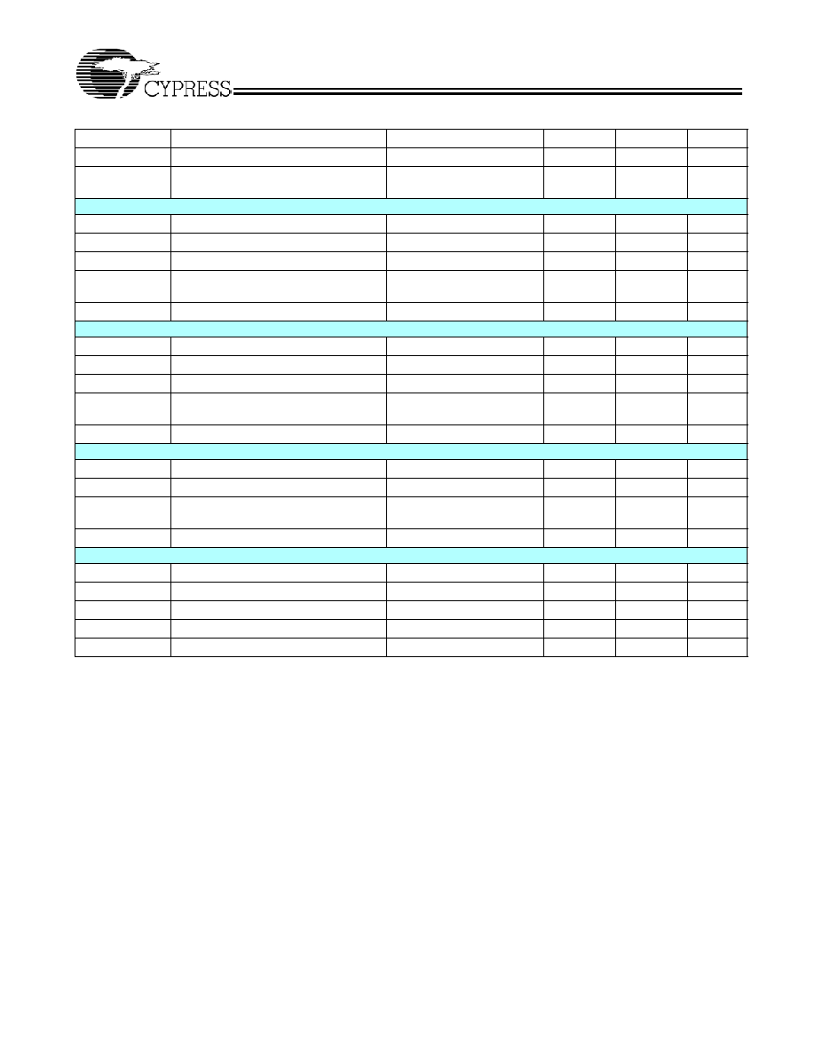
Test and Measurement Set-up
For Differential CPU Output Signals
The following diagram shows lumped test load configurations
for the differential Host Clock Outputs.
Table 7. Group Timing Relationship and Tolerances
Offset (Typical)
Tolerance (or Range)
Conditions
Notes
CPU to AGP
2 ns
1 ≠ 4 ns
CPU leads
≠
CPU to Z
2 ns
1 ≠ 4 ns
CPU leads
≠
CPU to PCI
2 ns
1 ≠ 4 ns
CPU leads
≠
C P U T /C
T
P C B
68
M easurem ent P oint
5pF
V D D _C P U
C P U C S
T
P C B
75
M easurem ent P oint
5pF
V D D _C P U
Figure 7. CPUCLK Test Load Configuration
2 .4 V
0 .4 V
3 .3 V
0 V
T r
T f
1 .5 V
3 .3 V s ig n a ls
tD C
P r o b e
O u tp u t u n d e r T e s t
L o a d C a p
-
-
Figure 8. Lumped Load For Single-Ended Output Signals (for AC Parameters Measurement)
CY28372
Document #: 38-07533 Rev. *A
Page 16 of 18
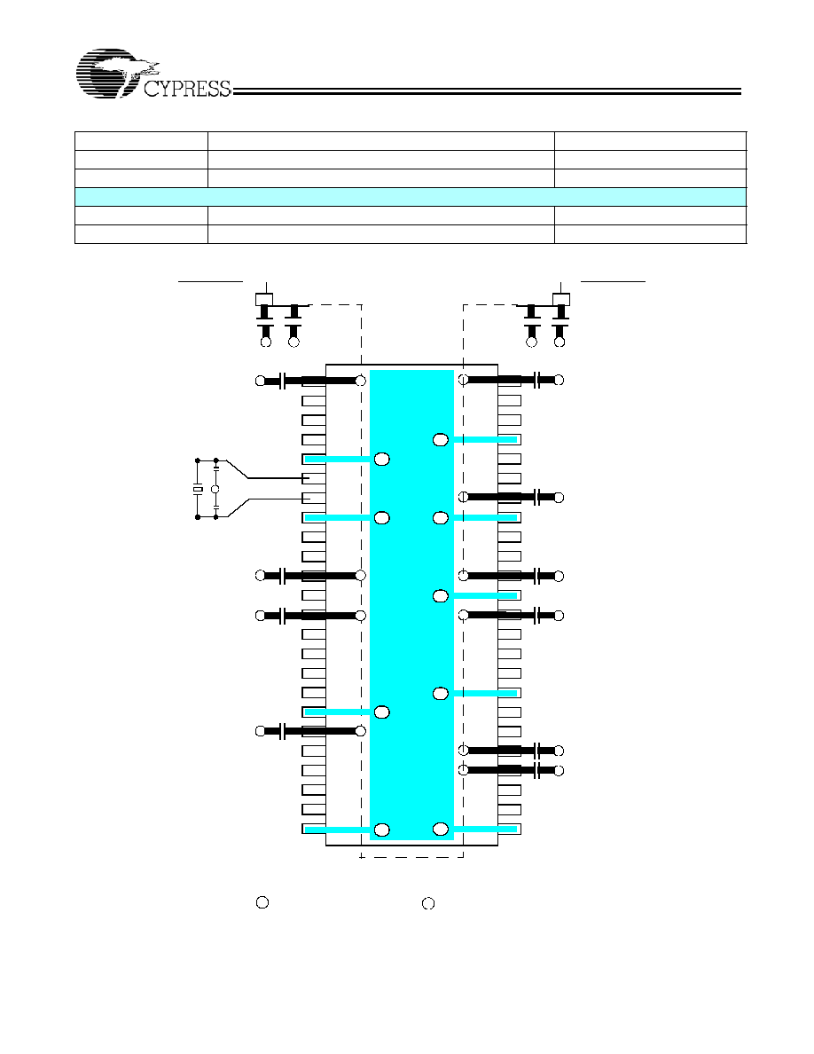
Layout Example
Ordering Information
Ordering Code
Package Type
Operating Range
CY28372OC
48-pin Small Shrunk Outline Package (SSOP)
Commercial, 0∞C to 70∞C
CY28372OCT
48-pin Small Shrunk Outline Package (SSOP) ≠ Tape and Reel Commercial, 0∞C to 70∞C
Lead Free
CY28372OXC
48-pin Small Shrunk Outline Package (SSOP)
Commercial, 0∞C to 70∞C
CY28372OXCT
48-pin Small Shrunk Outline Package (SSOP) ≠ Tape and Reel Commercial, 0∞C to 70∞C
G
FB
G
G
VDD33
C2
48
47
46
45
44
43
42
41
40
38
37
36
35
34
33
32
31
30
29
28
27
26
25
1
2
3
4
5
6
7
8
9
10
11
12
13
14
15
16
17
18
19
20
21
22
23
24
39
G
V
G
V
G
V
G
V
G
V
G
V
G = VIA to GND plane layer
V
Note: Each supply plane or strip should have a ferrite bead and capacitors
Cermaic Caps C1 = 10 - 22 µF
C2 = .005 µF
FB = Dale ILB1206 - 300 (300
@ 100 MHz)
C3 = .1
µF
All bypass caps = .1-
µf ceramic
* For use with onboard video using 48 MHz for Dot Clock or connect to VDDQ3
G
V
FB
G
G
VDD25
C2
G
V
G
V
G
V
G
G
G
G
G
G
G
G
G
CY2
8372
C1
C1
C3
C3
C3
C3
C3
C3
C3
C3
C3
C3
= VIA to respective supply plane layer
CY28372
Document #: 38-07533 Rev. *A
Page 17 of 18
© Cypress Semiconductor Corporation, 2004. The information contained herein is subject to change without notice. Cypress Semiconductor Corporation assumes no responsibility for the use
of any circuitry other than circuitry embodied in a Cypress product. Nor does it convey or imply any license under patent or other rights. Cypress products are not warranted nor intended to be
used for medical, life support, life saving, critical control or safety applications, unless pursuant to an express written agreement with Cypress. Furthermore, Cypress does not authorize its
products for use as critical components in life-support systems where a malfunction or failure may reasonably be expected to result in significant injury to the user. The inclusion of Cypress
products in life-support systems application implies that the manufacturer assumes all risk of such use and in doing so indemnifies Cypress against all charges.
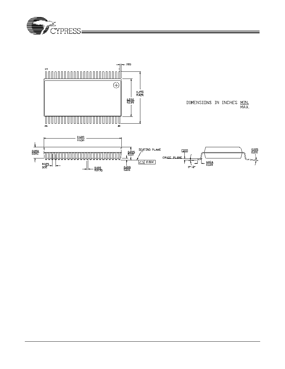
Package Diagram
Purchase of I
2
C components from Cypress, or one of its sublicensed Associated Companies, conveys a license under the Philips
I
2
C Patent Rights to use these components in an I
2
C system, provided that the system conforms to the I
2
C Standard Specification
as defined by Philips. Athlon and Duron are trademarks of Advanced Micro Devices, Inc. Dial-A-Frequency is a registered
trademark of Cypress Semiconductor. All product and company names mentioned in this document are the trademarks of their
respective holders.
48-lead Shrunk Small Outline Package O48
51-85061-*C

CY28372
Document #: 38-07533 Rev. *A
Page 18 of 18
Document History Page
Document Title: CY28372 SiS 746 AMD AthlonTM/AMD DuronTM Clock Synthesizer
Document Number: 38-07533
REV.
ECN NO. Issue Date
Orig. of
Change
Description of Change
**
125162
04/25/03
RGL
New data sheet
*A
266732
See ECN
RGL
Added Lead-Free devices