 | –≠–ª–µ–∫—Ç—Ä–æ–Ω–Ω—ã–π –∫–æ–º–ø–æ–Ω–µ–Ω—Ç: CY28400 | –°–∫–∞—á–∞—Ç—å:  PDF PDF  ZIP ZIP |
100-MHz Differential Buffer for PCI Express and SATA
CY28400
Cypress Semiconductor Corporation
∑
3901 North First Street
∑
San Jose
,
CA 95134
∑
408-943-2600
Document #: 38-07591 Rev. **
Revised November 24, 2003
Features
∑ CK409 or CK410 companion buffer
∑ Four differential 0.7v clock pairs
∑ Individual OE controls
∑ Low CTC jitter (< 50 ps)
∑ Programmable bandwidth
∑ SRC_STOP# power management control
∑ SMBus Block/Byte/Word Read and Write support
∑ 3.3V operation
∑ PLL Bypass-configurable
∑ Divide by 2 programmable outputs
∑ 28-pin SSOP package
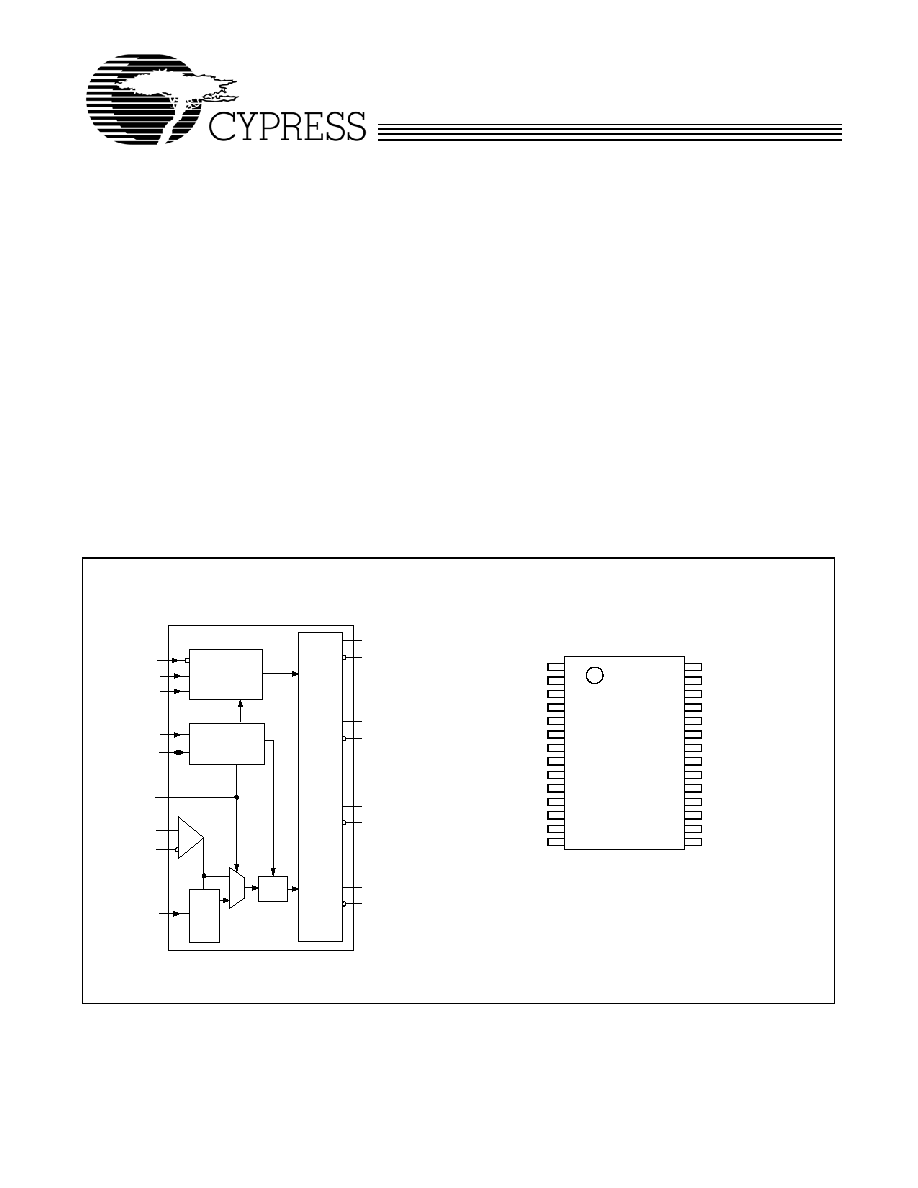
Functional Description
The CY28400 is a differential buffer and serves as a
companion device to the CK409 or CK410 clock generator.
The device is capable of distributing the Serial Reference
Clock (SRC) in PCI Express and SATA implementations.
Block Diagram
Pin Configuration
PLL/BYPASS#
DIFT2
DIFC2
DIFT1
DIFC1
DIFT5
DIFC5
DIFT6
DIFC6
Output
Buffer
Output
Control
PLL
DIV
SMBus
Controller
SRC_STOP#
PWRDWN#
SCLK
SDATA
SRCT_IN
SRCC_IN
HIGH_BW#
OE_(1,6)
28 SSOP
VDD
SRCT_IN
VSS
VDD
DIFT1
DIFC1
OE_1
DIFT2
DIFC2
VDD
PLL/BYPASS#
SCLK
SDATA
VDD_A
VSS_A
SRC_STOP#
PWRDWN#
HIGH_BW#
DIFC5
VDD
DIFT5
DIFC6
0E_6
DIFT6
VSS
VDD
IREF
28
27
26
25
24
23
22
21
20
19
18
17
16
15
1
2
3
4
5
6
7
8
9
10
11
12
13
14
CY28400
SRCC_IN
CY28400
Document #: 38-07591 Rev. **
Page 2 of 14
Pin Descriptions
Serial Data Interface
To enhance the flexibility and function of the clock synthesizer,
a two-signal serial interface is provided. Through the Serial
Data Interface, various device functions, such as individual
clock output buffers, can be individually enabled or disabled.
The registers associated with the Serial Data Interface
initializes to their default setting upon power-up, and therefore
use of this interface is optional. Clock device register changes
are normally made upon system initialization, if any are
required. The interface cannot be used during system
operation for power management functions.
Data Protocol
The clock driver serial protocol accepts byte write, byte read,
block write, and block read operations from the controller. For
block write/read operation, the bytes must be accessed in
sequential order from lowest to highest byte (most significant
bit first) with the ability to stop after any complete byte has
been transferred. For byte write and byte read operations, the
system controller can access individually indexed bytes. The
offset of the indexed byte is encoded in the command code,
as described in Table 1.
The block write and block read protocol is outlined in Table 2
while Table 3 outlines the corresponding byte write and byte
read protocol. The slave receiver address is 11011100 (DCh).
Pin
Name
Type
Description
2,3
SRCT_IN, SRCC_IN I,DIF
0.7V differential SRC inputs from the clock synthesizer
6,7,9,10,19,20,22,23
DIFT/C(2:1) & (6:5)
O,DIF
0.7V differential clock outputs
8,21
OE_1, OE_6
I,SE
3.3V LVTTL active low input for three-stating differential outputs
(DIFT2 and DIFT5 are unaffected by the assertion of OE inputs)
17
HIGH_BW#
I,SE
3.3V LVTTL input for selecting PLL bandwidth
16
SRC_STOP#
I,SE
3.3V LVTTL input for SRC_STOP#, active low
15
PWRDWN#
I,SE
3.3V LVTTL input for Power Down, active low
13
SCLK
I,SE
SMBus slave clock input
14
SDATA
I/O,OC
Open collector SMBus data
26
IREF
I
A precision resistor is attached to this pin to set the differential
output current
12
PLL/BYPASS#
I
3.3V LVTTL input for selecting fan-out or PLL operation
28
VDD_A
3.3V
3.3V power supply for PLL
27
VSS_A
GND
Ground for PLL
4,25
VSS
3.3V
Ground for outputs
1,5,11,18,24
VDD
GND
3.3V power supply for outputs
Table 1. Command Code Definition
Bit
Description
7
0 = Block read or block write operation
1 = Byte read or byte write operation
(6:0)
Byte offset for byte read or byte write operation. For block read or block write operations, these bits should be
'0000000'
Table 2. Block Read and Block Write Protocol
Block Write Protocol
Block Read Protocol
Bit
Description
Bit
Description
1
Start
1
Start
2:8
Slave address ≠ 7 bits
2:8
Slave address ≠ 7 bits
9
Write = 0
9
Write = 0
10
Acknowledge from slave
10
Acknowledge from slave
11:18
Command Code ≠ 8 bits
'00000000' stands for block operation
11:18
Command Code ≠ 8 bits
'00000000' stands for block operation
19
Acknowledge from slave
19
Acknowledge from slave
20:27
Byte Count from master ≠ 8 bits
20
Repeat start
CY28400
Document #: 38-07591 Rev. **
Page 3 of 14
28
Acknowledge from slave
21:27
Slave address ≠ 7 bits
29:36
Data byte 0 from master ≠ 8 bits
28
Read = 1
37
Acknowledge from slave
29
Acknowledge from slave
38:45
Data byte 1 from master ≠ 8 bits
30:37
Byte count from slave ≠ 8 bits
46
Acknowledge from slave
38
Acknowledge from host
....
Data bytes from master/Acknowledge
39:46
Data byte 0 from slave ≠ 8 bits
....
Data Byte N ≠ 8 bits
47
Acknowledge from host
....
Acknowledge from slave
48:55
Data byte 1 from slave ≠ 8 bits
....
Stop
56
Acknowledge from host
....
Data bytes from slave/Acknowledge
....
Data byte N from slave ≠ 8 bits
....
Acknowledge from host
....
Stop
Table 3. Byte Read and Byte Write Protocol
Byte Write Protocol
Byte Read Protocol
Bit
Description
Bit
Description
1
Start
1
Start
2:8
Slave address ≠ 7 bits
2:8
Slave address ≠ 7 bits
9
Write = 0
9
Write = 0
10
Acknowledge from slave
10
Acknowledge from slave
11:18
Command Code ≠ 8 bits
'100xxxxx' stands for byte operation, bits[6:0] of the
command code represents the offset of the byte to be
accessed
11:18
Command Code ≠ 8 bits
'100xxxxx' stands for byte operation, bits[6:0]
of the command code represents the offset of
the byte to be accessed
19
Acknowledge from slave
19
Acknowledge from slave
20:27
Data byte from master ≠ 8 bits
20
Repeat start
28
Acknowledge from slave
21:27
Slave address ≠ 7 bits
29
Stop
28
Read = 1
29
Acknowledge from slave
30:37
Data byte from slave ≠ 8 bits
38
Acknowledge from master
39
Stop
Byte 0: Control Register 0
Bit
@Pup
Name
Description
7
0
PWRDWN# drive mode
o = Driven when stopped, 1 = Three-state
6
0
SRC_STOP# drive mode
o = Driven when stopped, 1 = Three-state
5
0
Reserved
4
0
Reserved
3
0
Reserved
2
1
HIGH_BW#
HIGH_BW#
0 = High Bandwidth, 1 = Low bandwidth
Table 2. Block Read and Block Write Protocol (continued)
Block Write Protocol
Block Read Protocol
Bit
Description
Bit
Description
CY28400
Document #: 38-07591 Rev. **
Page 4 of 14
1
1
PLL/Bypass#
PLL/Bypass#
0 = Fanout buffer, 1 = PLL mode
0
1
SRC_DIV/2
0 = Divided by 2 mode,1 = Normal (output = input)
Byte 1: Control Register 1
Bit
@Pup
Name
Description
7
1
Reserved
6
1
DIFT/C6
DIFT/C6 Output Enable
0 = Disabled (three-state), 1 = Enabled
5
1
DIFT/C5
DIFT/C5 Output Enable
0 = Disabled (three-state), 1 = Enabled
4
1
Reserved
3
1
Reserved
2
1
DIFT/C2
DIFT/C2 Output Enable
0 = Disabled (three-state), 1 = Enabled
1
1
DIFT/C1
DIFT/C1 Output Enable
0 = Disabled (three-state), 1 = Enabled
0
1
Reserved
Byte 2: Control Register 2
Bit
@Pup
Name
Description
7
0
Reserved
6
0
Allow Control DIFT/C6 with assertion of SRC_STOP#
0 = Free-running, 1 = Stopped with SRC_STOP#
5
0
Allow Control DIFT/C5 with assertion of SRC_STOP#
0 = Free-running, 1 = Stopped with SRC_STOP#
4
0
Reserved
3
0
Reserved
2
0
Allow Control DIFT/C2 with assertion of SRC_STOP#
0 = Free-running, 1 = Stopped with SRC_STOP#
1
0
Allow Control DIFT/C1 with assertion of SRC_STOP#
0 = Free-running, 1 = Stopped with SRC_STOP#
0
0
Reserved
Byte 3: Control Register 3
Bit
@Pup
Name
Description
7
0
Reserved
6
0
Reserved
5
0
Reserved
4
0
Reserved
3
0
Reserved
2
0
Reserved
1
0
Reserved
0
0
Reserved
Byte 0: Control Register 0 (continued)
Bit
@Pup
Name
Description
CY28400
Document #: 38-07591 Rev. **
Page 5 of 14
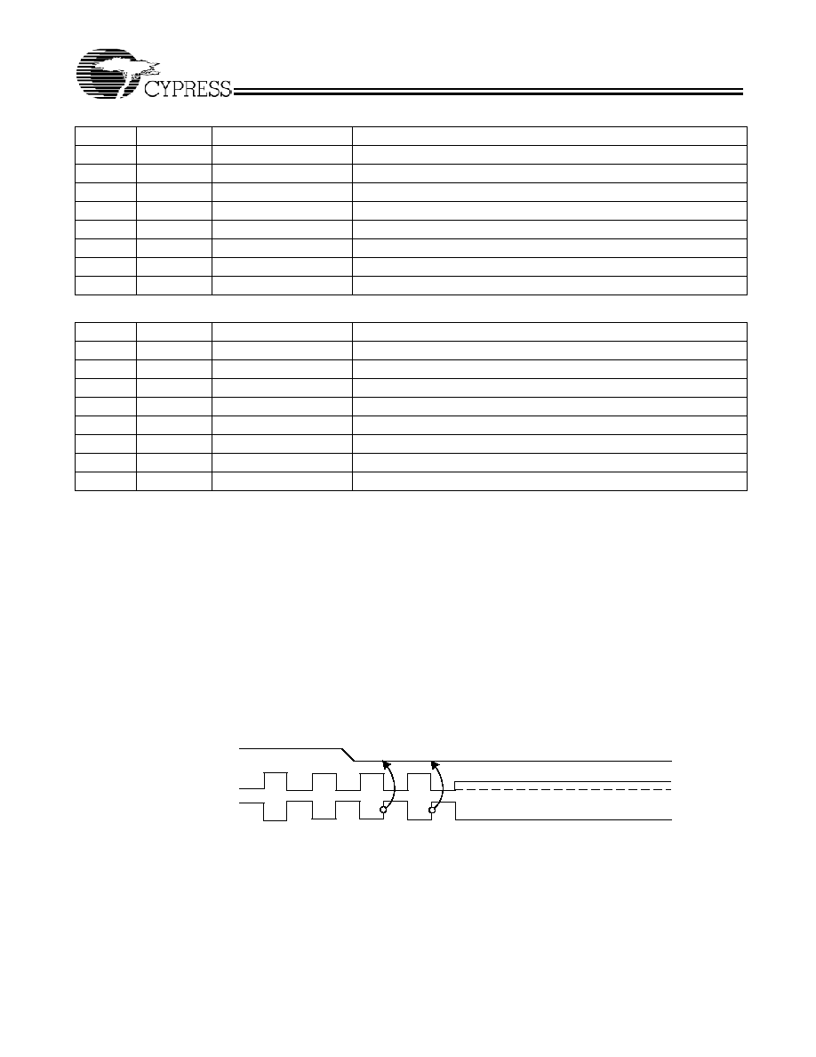
PWRDWN# Clarification
[1]
The PWRDWN# pin is used to shut off all clocks cleanly and
instruct the device to evoke power savings mode. Additionally,
PWRDWN# should be asserted prior to shutting off the input
clock or power to ensure all clocks shut down in a glitch-free
manner. PWRDWN# is an asynchronous active low input. This
signal is synchronized internal to the device prior to powering
down the clock buffer. PWRDWN# is an asynchronous input
for powering up the system. When PWRDWN# is asserted
low, all clocks will be held high or three-stated (depending on
the state of the control register drive mode and OE bits) prior
to turning off the VCO. All clocks will start and stop without any
abnormal behavior and must meet all AC and DC parameters.
This means no glitches, frequency shifting or amplitude abnor-
malities among others.
PWRDWN#--Assertion
When PWRDWN# is sampled low by two consecutive rising
edges of DIFC, all DIFT outputs will be held high or
three-stated (depending on the state of the control register
drive mode and OE bits) on the next DIFC high to low
transition. When the SMBus power-down drive mode bit is
programmed to `0', all clock outputs will be held with the DIFT
pin driven high at 2 x Iref and DIFC three-state. However, if the
control register PWRDWN# drive mode bit is programmed to
`1', then both DIFT and the DIFC are three-stated.
Note:
1. Disabling of the SRCT_IN input clock prior to assertion of PWRDWN# is an undefined mode and not recommended. Operation in this mode may result in glitches
excessive frequency shifting.
Byte 4: Vendor ID Register
Bit
@Pup
Name
Description
7
0
Revision Code Bit 3
6
0
Revision Code Bit 2
5
0
Revision Code Bit 1
4
0
Revision Code Bit 0
3
1
Vendor ID Bit 3
2
0
Vendor ID Bit 2
1
0
Vendor ID Bit 1
0
0
Vendor ID Bit 0
Byte 5: Control Register 5
Bit
@Pup
Name
Description
7
0
Reserved
6
0
Reserved
5
0
Reserved
4
0
Reserved
3
0
Reserved
2
0
Reserved
1
0
Reserved
0
0
Reserved
PWRDWN#
DIFC
DIFT
Figure 1. PWRDWN# Assertion Diagram
CY28400
Document #: 38-07591 Rev. **
Page 6 of 14
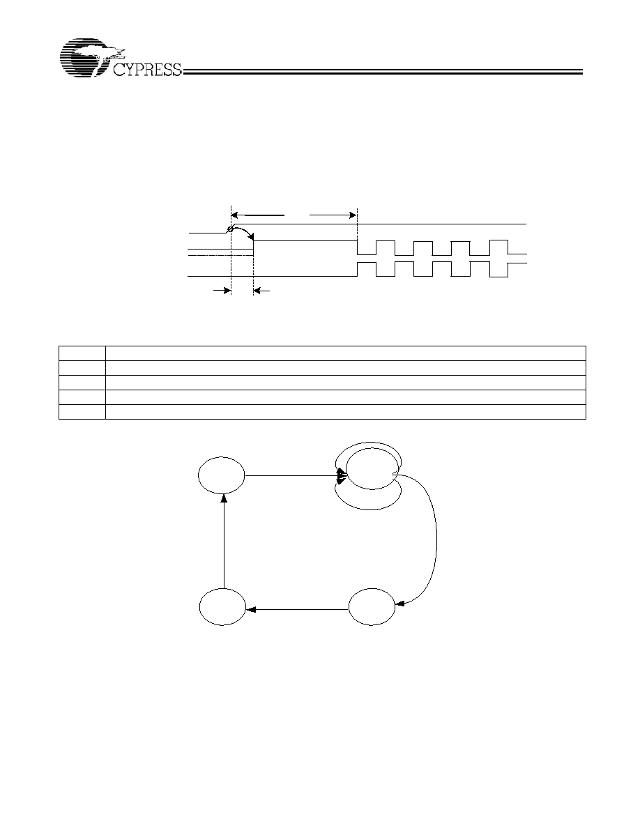
PWRDWN#--Deassertion
The power-up latency is less than 1ms. This is the time from
the deassertion of the PWRDWN# pin or the ramping of the
power supply or the time from valid SRC_IN input clocks until
the time that stable clocks are output from the buffer chip (PLL
locked). If the control register PWRDWN# three-state bit is
programmed to `1', all differential outputs will be driven high in
less than 300
µS of PWRDWN# deassertion to a voltage
greater than 200 mV.
Notes:
2. The total power up latency from power on to all outputs active is less than 1 ms (assuming a valid clock is present on SRC_IN input).
3. If power is valid and PWRDWN# is deasserted but no input clocks are present on the SRC_IN input, DIF clocks will remain disabled. Only after valid input clocks
are detected, valid power, PWRDWN# deasserted with the PLL locked and stable are the DIF outputs enabled.
Table 4. Buffer Power-Up State Machine
State
Description
0
3.3V Buffer power off
1
After 3.3V supply is detected to rise above 1.8V≠2.0V, the buffer enters state 1 and initiates a 0.2-ms≠0.3-ms delay
2
[3]
Buffer waits for a valid clock on the SRC_IN input and PWRDWN# deassertion
3
[2]
Once the PLL is locked to the SRC_IN input clock, the buffer enters state 3 and enables outputs for normal operation
DIFC
DIFT
Tstable
<1mS
PWRDWN#
Tdrive_Pwrdwn#
<300uS, >200mV
Figure 2. PWRDWN# Deassertion Diagram
S2
Wait for Input
Clock &
PWRDWN# De-
assertion
PWRDWN# Asserted
S1
Delay
>0.25ms
S0
Power Off
S3
Normal
Operation
No Input Clock
Figure 3. Buffer Power-up State Diagram
CY28400
Document #: 38-07591 Rev. **
Page 7 of 14
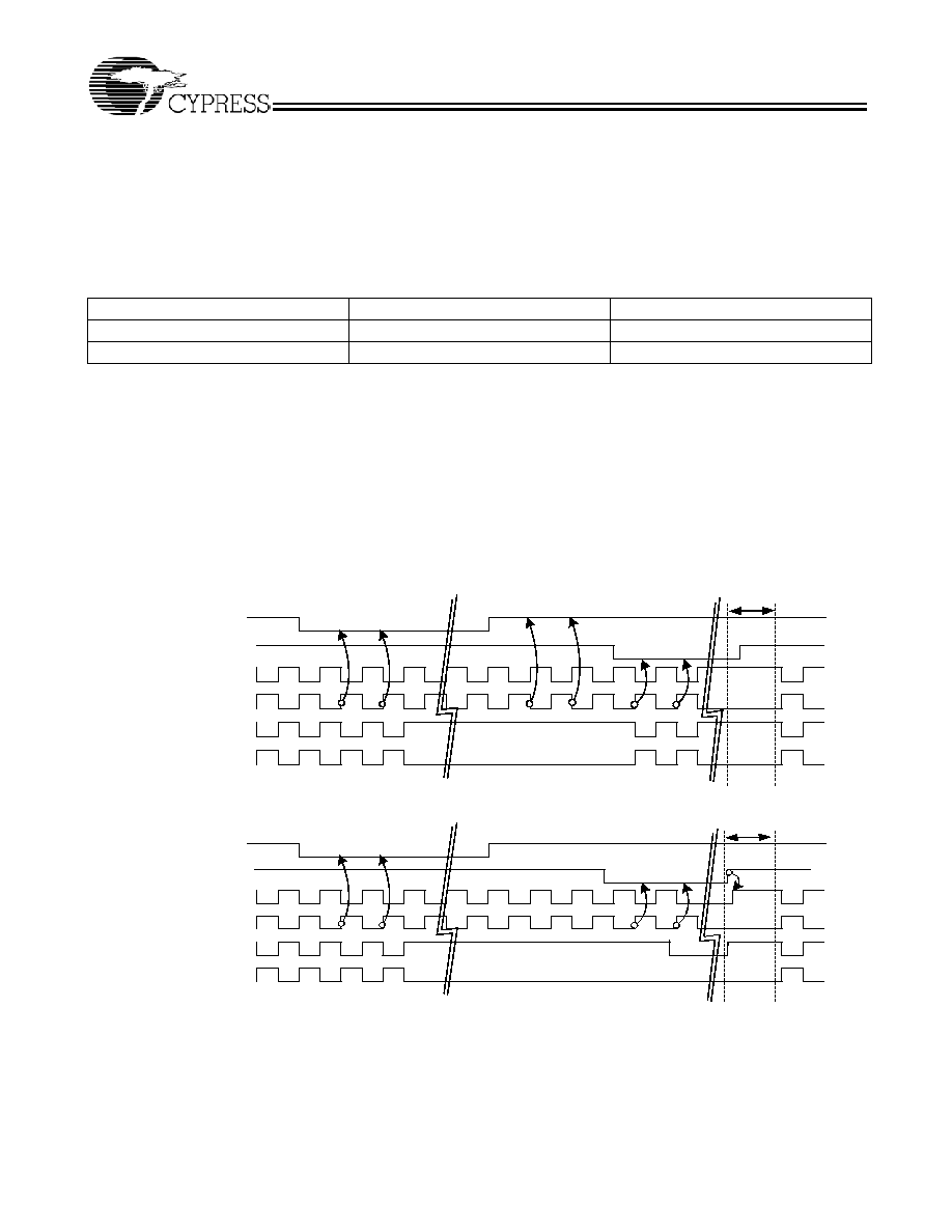
SRC_STOP# Clarification
The SRC_STOP# signal is an active low input used for clean
stopping and starting the DIF outputs (valid clock must be
present on SRCT_IN). The SRC_STOP# signal is a
de-bounced signal in that it's state must remain unchanged
during two consecutive rising edges of DIFC to be recognized
as a valid assertion or deassertion. (The assertion and
deassertion of this signal is absolutely asynchronous).
SRC_STOP# Assertion
The impact of asserting the SRC_STOP# pin is all DIF outputs
that are set in the control registers to stoppable via assertion
of SRC_STOP# are stopped after their next transition. When
the control register SRC_STOP# three-state bit is
programmed to `0', the final state of all stopped DIFT/C signals
is DIFT clock = High and DIFC = Low. There is to be no change
to the output drive current values, DIFT will be driven high with
a current value equal 6 x Iref, and DIFC will not be driven.
When the control register SRC_STOP# three-state bit is
programmed to `1', the final state of all stopped DIF signals is
low, both DIFT clock and DIFC clock outputs will not be driven.
SRC_STOP# Deassertion
All differential outputs that were stopped will resume normal
operation in a glitch-free manner. The maximum latency from
the deassertion to active outputs is between 2≠6 DIFT/C clock
periods (two clocks are shown) with all DIFT/C outputs
resuming simultaneously. If the control register three-state bit
is programmed to `1' (three-state), then all stopped DIFT
outputs will be driven high within 10 ns of SRC_STOP#
deassertion to a voltage greater than 200 mV.
Note:
4. In the case where OE is asserted high, the output will always be three-stated regardless of SRC_STOP# drive mode register bit state.
Table 5. SRC_STOP# Functionality
[4]
SRC_STOP#
DIFT
DIFC
1
Normal
Normal
0
Iref * 6 or Float
Low
DIFC (Stoppable)
DIFT (Stoppable)
DIFC(Free Running
DIFT(Free Running
PWRDWN#
1mS
SRC_STOP#
Figure 4. SRC_STOP# = Driven, PWRDWN# = Driven
DIFC (Stoppable)
DIFC(Free Running
PWRDWN#
1mS
SRC_STOP#
DIFT (Stoppable)
DIFT(Free Running
Figure 5. SRC_STOP# =Driven, PWRDWN# = Three-state
CY28400
Document #: 38-07591 Rev. **
Page 8 of 14
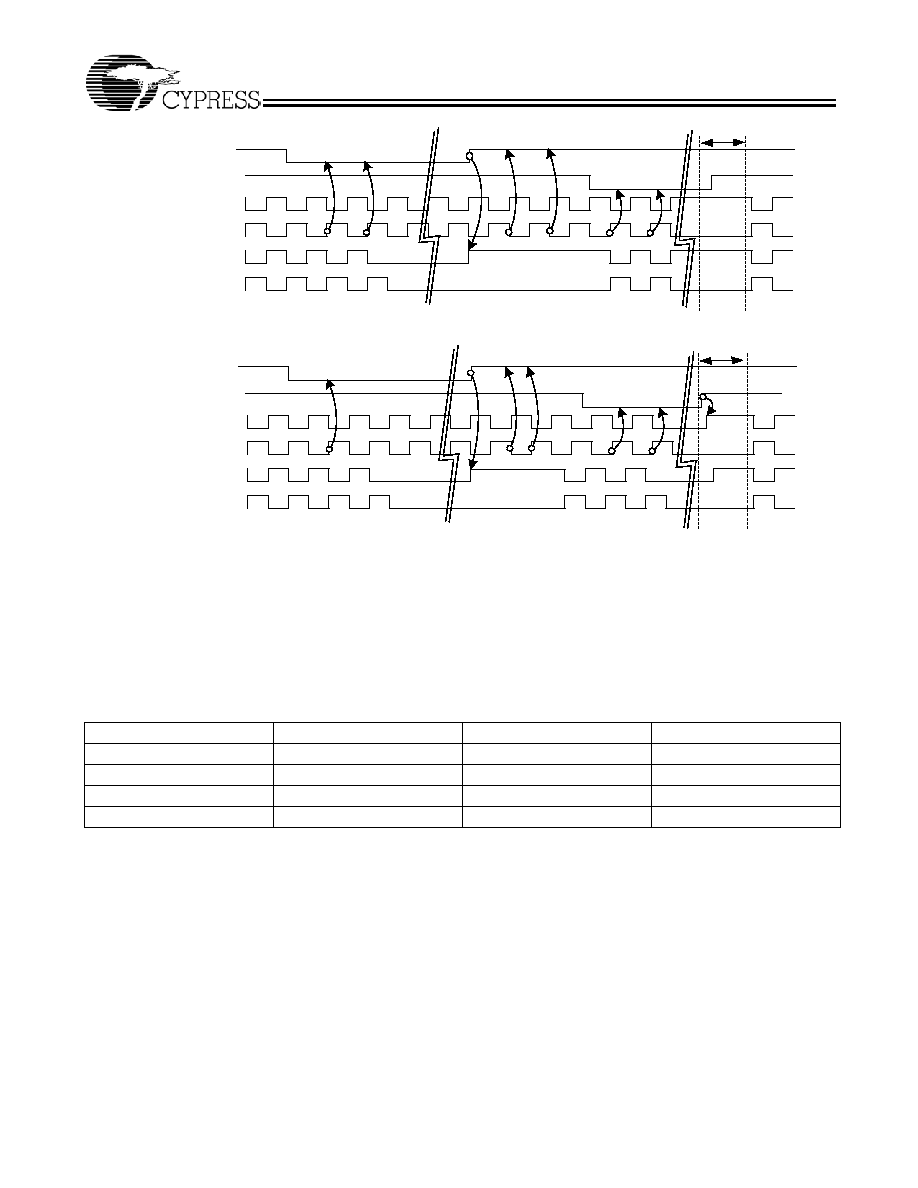
Output Enable Clarification
The outputs may be disabled in two ways, via writing a `0' to
SMBus register bit corresponding to output of interest or by
asserting an OE input pin low. In both methods, if SMBus
registered bit has been written low or the OE pin is low or both,
the output of interest will be three-stated. The assertion and
deassertion of this signal is asynchronous.
OE Assertion
(Transition from `0' to `1')
All differential outputs that were three-stated will resume
normal operation in a glitch-free manner. The maximum
latency from the assertion to active outputs is between 2≠6 DIF
clock periods. In addition, DIFT clocks will be driven high within
10 ns of OE assertion to a voltage greater than 200 mV.
OE Deassertion
(Transition from `1' to `0')
The impact of de- asserting OE is each corresponding output
will transition from normal operation to three-state in a
glitch-free manner. The maximum latency from the
deassertion to three-stated outputs is between 2≠6 DIF clock
periods.
SRC_DIV2# Clarification
The SRC_DIV2# feature is used to configure the DIF output
mode to be equal to the SRCT_IN input frequency or half the
input frequency in a glitch-free manner. The SRC_DIV2#
function may be implemented by writing a `0' to SMBus register
bit.
SRC_DIV2# Assertion
The impact of writing a `0' to the SRC_DIV/2 register bit is all
DIF outputs will transition cleanly in a glitch-free manner from
normal operation (output frequency equal to input) to half the
input frequency within 2≠6 DIF clock periods.
DIFC (Stoppable)
DIFC(Free Running
DIFT(Free Running
PWRDWN#
1mS
SRC_STOP#
DIFT (Stoppable)
Figure 6. SRC_STOP# = Three-state, PWRDWN# = Driven
DIFC(Free Running
DIFT(Free Running
DIFT (Stoppable)
DIFC (Stoppable)
PWRDWN#
1mS
SRC_STOP#
Figure 7. SRC_STOP# = Three-state, PWRDWN# = Three-state
Table 6. OE Functionality
OE (Pin)
OE (SMBus Bit)
DIFT
DIFC
1
1
Normal
Normal
1
0
Three-state
Three-state
0
1
Three-state
Three-state
0
0
Three-state
Three-state

CY28400
Document #: 38-07591 Rev. **
Page 9 of 14
SRC_DIV2# Deassertion
The impact of writing a `0' to the SRC_DIV/2 register bit is all
DIF outputs will transition cleanly in a glitch-free manner from
divide by 2 mode to normal (output frequency is equal to the
input frequency) operation within 2≠6 DIF clock periods.
PLL/BYPASS# Clarification
The PLL/Bypass# input is used to select between bypass
mode (no PLL) and PLL mode. In bypass mode, the input clock
is passed directly to the output stage resulting in 50ps additive
jitter (50 ps + input jitter) on DIF outputs. In the case of PLL
mode, the input clock is pass through a PLL to reduce high
frequency jitter. The BYPASS# mode may be selected in two
ways, via writing a `0' to SMBus register bit or by asserting the
PLL/BYPASS# pin low. In both methods, if the SMBus register
bit has been written low or PLL/BYPASS# pin is low or both,
the device will be configure for BYPASS operation.
HIGH_BW# Clarification
The HIGH_BW# input is used to set the PLL bandwidth. This
mode is intended to minimize PLL peaking when two or more
buffers are cascaded by staggering device bandwidths. The
PLL low bandwidth mode may be selected in two ways, via
writing a `0' to SMBus register bit or by asserting the
HIGH_BW# pin is low or both, the device will be configured for
low bandwidth operation.
CY28400
Document #: 38-07591 Rev. **
Page 10 of 14
Absolute Maximum Conditions
Parameter
Description
Condition
Min.
Max.
Unit
V
DD
Core Supply Voltage
≠0.5
4.6
V
V
DD_A
Analog Supply Voltage
≠0.5
4.6
V
V
IN
Input Voltage
Relative to V
SS
≠0.5
V
DD
+ 0.5
VDC
T
S
Temperature, Storage
Non-functional
≠65
150
∞C
T
A
Temperature, Operating Ambient
Functional
0
70
∞C
T
J
Temperature, Junction
Functional
≠
150
∞C
ÿ
JC
Dissipation, Junction to Case
Mil-Spec 883E Method 1012.1
≠
TBD
∞C/W
ÿ
JA
Dissipation, Junction to Ambient
JEDEC (JESD 51)
≠
TBD
∞C/W
ESD
HBM
ESD Protection (Human Body Model)
MIL-STD-883, Method 3015
2000
≠
V
UL-94
Flammability Rating
At 1/8 in.
V≠0
MSL
Moisture Sensitivity Level
1
Multiple Supplies: The Voltage on any input or I/O pin cannot exceed the power pin during power-up. Power supply sequencing
is NOT required.
DC Electrical Specifications
Parameter
Description
Condition
Min.
Max.
Unit
V
DD_A
, V
DD
3.3V Operating Voltage
3.3 ± 5%
3.135
3.465
V
V
ILI2C
Input Low Voltage
SDATA, SCLK
≠
1.0
V
V
IHI2C
Input High Voltage
SDATA, SCLK
2.2
≠
V
V
IL
3.3V Input Low Voltage
V
SS
≠ 0.5
0.8
V
V
IH
3.3V Input High Voltage
2.0
V
DD
+ 0.5
V
I
IL
Input Low Leakage Current
except internal pull-up resistors, 0 < V
IN
< V
DD
≠5
µA
I
IH
Input High Leakage Current
except internal pull-down resistors, 0 < V
IN
< V
DD
5
µA
I
OZ
High-impedance Output Current
≠10
10
µA
C
IN
Input Pin Capacitance
2
5
pF
C
OUT
Output Pin Capacitance
3
6
pF
L
IN
Pin Inductance
≠
7
nH
I
DD3.3V
Dynamic Supply Current
At max. load and 100 MHz per Figure 8
≠
215
mA
I
PD3.3V
Power-down Supply Current
PD asserted, Outputs driven
≠
40
mA
I
PD3.3V
Power-down Supply Current
PD asserted, Outputs Three-stated
≠
5
mA
AC Electrical Specification
Parameter
Description
Condition
Min.
Max.
Unit
DIF at 0.7V
T
DC
DIFT and DIFC Duty Cycle
Measured at crossing point V
OX
45
55
%
T
SKEW
Any DIFT/C to DIFT/C Clock Skew, SSC Measured at crossing point V
OX
≠
150
ps
T
PERIOD
Average Period
Measured at crossing point V
OX
at 100 MHz
9.9970
10.0533
ns
T
CCJ
DIFT/C Cycle to Cycle Jitter
Measured at crossing point V
OX
≠
50
ps
T
R
/ T
F
DIFT and DIFC Rise and Fall Times
Measured from V
OL
= 0.175 to V
OH
= 0.525V
175
700
ps
T
RFM
Rise/Fall Matching
Determined as a fraction of 2*(T
R
≠ T
F
)/(T
R
+ T
F
)
≠
20
%
T
R
Rise Time Variation
≠
125
ps
T
F
Fall Time Variation
≠
125
ps
V
HIGH
Voltage High
Measured SE
660
850
mv
V
LOW
Voltage Low
Measured SE
≠150
≠
mv
CY28400
Document #: 38-07591 Rev. **
Page 11 of 14
Switching Waveforms
V
OX
Crossing Point Voltage at 0.7V Swing
250
550
mv
V
OX
Vcross Variation over all edges
≠
140
mV
V
OVS
Maximum Overshoot Voltage
≠
V
HIGH
+
0.3
V
V
UDS
Minimum Undershoot Voltage
≠
≠0.3
V
V
RB
Ring Back Voltage
Measured SE
0.2
N/A
V
t
PD(PLL)
Input to output skew in PLL mode
Measured at crossing point V
OX
≠
±250
ps
t
PD(NONPLL)
Input to output skew in Non - PLL mode Measured at crossing point V
OX
2.5
6.5
ns
AC Electrical Specification
(continued)
Parameter
Description
Condition
Min.
Max.
Unit
D IF T
T
P C B
T
P C B
D IF C
3 3
3 3
4 9 .9
4 9 .9
M e a s u r e m e n t
P o in t
2 p F
4 7 5
IR E F
M e a s u r e m e n t
P o in t
2 p F
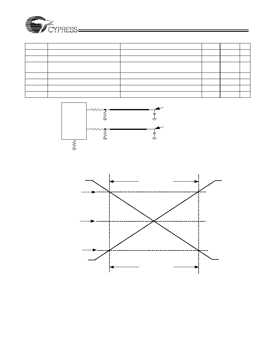
T r a c e Im p e d a n c e M e a s u r e d D iff e r e n tia lly
Figure 8. Differential Clock Termination
Figure 9. Single-Ended Measurement Points for TRise and TFall
V
OH
= 0.525V
TRise (CLOCK)
TFall (CLOCK)
CLO
CK#
V
OL
= 0.175V
VCROSS
CL
OC
K
CY28400
Document #: 38-07591 Rev. **
Page 12 of 14
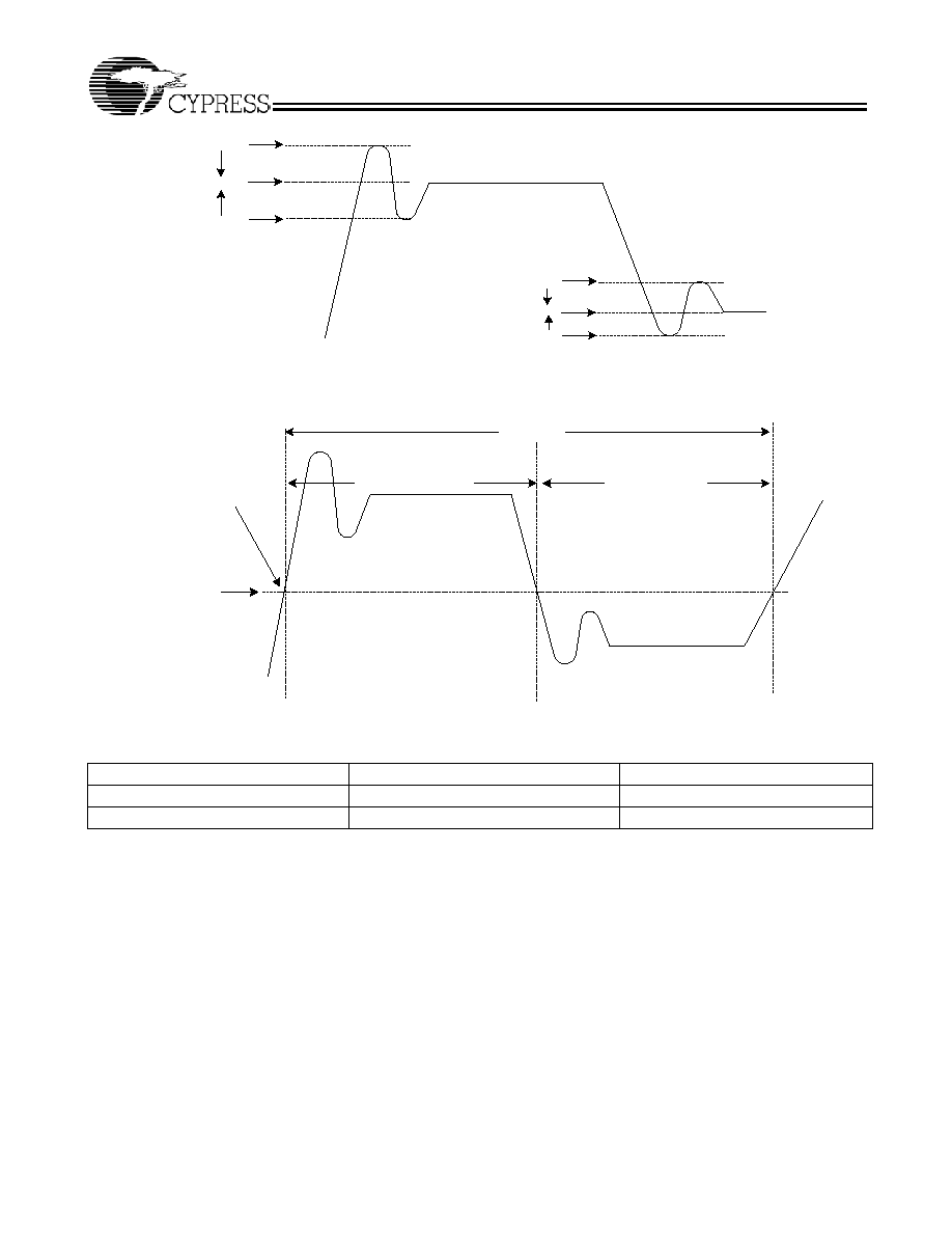
V
OVS
V
RB
V
LOW
V
UDS
V
RB
Figure 10. Single-ended Measurement Points for V
OVS
,V
UDS
and V
RB
0.000V
T
PERIOD
High Duty Cycle %
Low Duty Cycle %
Skew Management Point
Figure 11. Differential (Clock-CLock#) Measurement Points (Tperiod, Duty Cycle and Jitter)
Ordering Information
Ordering Code
Package Type
Operating Range
CY28400OC
28-pin SSOP
Commercial, 0∞C to 70 ∞C
CY28400OCT
28-pin SSOP (Tape & Reel)
Commercial, 0∞C to 70 ∞C
CY28400
Document #: 38-07591 Rev. **
Page 13 of 14
© Cypress Semiconductor Corporation, 2003. The information contained herein is subject to change without notice. Cypress Semiconductor Corporation assumes no responsibility for the use
of any circuitry other than circuitry embodied in a Cypress Semiconductor product. Nor does it convey or imply any license under patent or other rights. Cypress Semiconductor does not authorize
its products for use as critical components in life-support systems where a malfunction or failure may reasonably be expected to result in significant injury to the user. The inclusion of Cypress
Semiconductor products in life-support systems application implies that the manufacturer assumes all risk of such use and in doing so indemnifies Cypress Semiconductor against all charges.
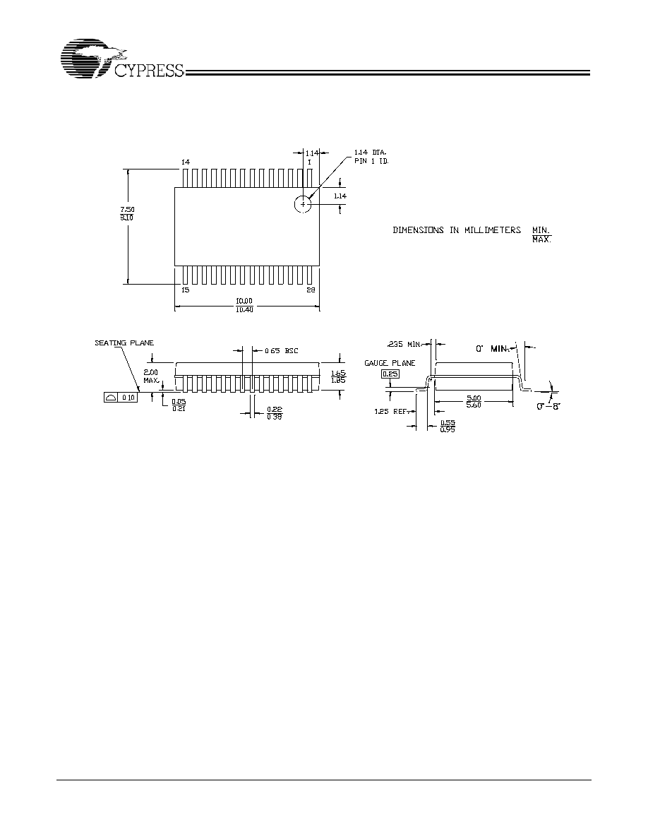
Package Drawing and Dimensions
All product and company names mentioned in this document may be the trademarks of their respective holders.
28-Lead (5.3 mm) Shrunk Small Outline Package O28
51-85079-*C

CY28400
Document #: 38-07591 Rev. **
Page 14 of 14
Document History Page
Document Title: CY28400 100-MHz Differential Buffer for PCI Express and SATA
Document Number: 38-07591
Rev.
ECN No.
Issue Date
Orig. of
Change
Description of Change
**
130190
11/26/03
RGL
New Data Sheet